
Ultra High-Density SOT-MRAM Design for Last-Level On-Chip Cache Application

1
Department of Information and Communication Engineering, Inha University, Incheon 22212, Republic of Korea
2
Department of Computer Engineering, Hongik University, Seoul 04066, Republic of Korea
*
Author to whom correspondence should be addressed.
Electronics 2023, 12(20), 4223; https://doi.org/10.3390/electronics12204223
Submission received: 27 August 2023
/
Revised: 25 September 2023
/
Accepted: 10 October 2023
/
Published: 12 October 2023
(This article belongs to the Special Issue Advances in Nanoelectronic, Nanomagnetic and Spintronic Device)
Abstract
:This paper presents ultra high-density spin-orbit torque magnetic random-access memory (SOT-MRAM) for last-level data cache application. Although SOT-MRAM has many appealing attributes of low write energy, nonvolatility, and high reliability, it poses challenges to ultra-high-density memory implementation. Due to using two access transistors per cell, the vertical dimension of SOT-MRAM is >40% longer than that of the spin-transfer torque magnetic random-access memory (STT-MRAM), a single transistor-based design. Moreover, the horizontal dimension cannot be reduced below two metal pitches due to the two vertical metal stacks per cell. This paper proposes an ultra-high-density SOT-MRAM design by reducing the vertical and horizontal dimensions. The proposed SOT-MRAM is designed by a single transistor with a Schottky diode to achieve lesser vertical dimension than the two-transistor-based design of conventional SOT-MRAM. Moreover, the horizontal dimension is also reduced by sharing a vertical metal between two consecutive bit-cells in the same row. The comparison of the proposed designs with the conventional SOT-MRAM reveals a 63% area reduction. Compared with STT-MRAM, the proposed high-density memory design achieves 48% higher integration density, 68% lower write power, 29% lower read power, and 1.9× higher read-disturb margin.
1. Introduction
Spin-transfer torque magnetic random-access memory (STT-MRAM) has garnered significant interest as an excellent prospect for on-chip cache memory applications, owing to its advantageous attributes, such as high integration density, low leakage power consumption, inherent nonvolatility, and compatibility with the complementary metal–oxide–semiconductor (CMOS) fabrication process [1,2,3,4,5,6,7,8,9,10].
A standard configuration of an STT-MRAM cell involves a single access transistor accompanied by a magnetic tunnel junction (MTJ) that serves as a storage element. Within this MTJ structure lies a pinned layer (PL) and a free layer (FL), sandwiching a tunneling oxide barrier, as depicted in Figure 1a. The magnetization of the PL is anchored in one direction, whereas that of the FL can be manipulated by passing an electrical current. The FL magnetization conventionally rests in two distinct states: parallel (P) or antiparallel (AP) with respect to the PL orientation. The antiparallel state results in a higher MTJ resistance than the parallel state, enabling a read operation by sensing the MTJ resistance difference. The STT-MRAM can have a high integration density exceeding twice that of conventional static RAM [11]. Furthermore, STT-MRAM effectively curtails the overall power consumption by obviating leakage concerns due to the nonvolatility of MTJ [10].
Despite its favorable features, STT-MRAM raises two points of concern regarding its reliability. First, the read current path aligns with the write current path, as illustrated in Figure 1b, introducing a compromise between read stability and writability. For example, a wider access transistor width, which ensures reliable write operations, increases the vulnerability to unintended bit flips during read operations, commonly referred to as read-disturb failures (Figure 1c) [9]. Second, achieving a high-speed write operation necessitates the application of a substantial electrical current, exposing the tunneling oxide barrier to significant stress conditions [11].
Recently, spin-orbit torque magnetic random-access memory (SOT-MRAM) has emerged as an alternative on-chip memory solution, demonstrating enhanced reliability [11,12,13,14,15,16,17,18,19,20,21]. The three-terminal configuration of SOT-MRAM segregates the write and read paths, enabling independent optimization of the read stability and writability [15]. Additionally, in SOT-MRAM, the write mechanism circumvents the need for imposing high stress on the tunneling oxide barrier. Instead, it leverages spin injection from a heavy metal (HM) [11]. Furthermore, in contrast to STT-MRAM, SOT-MRAM holds more potential for energy-efficient write operations, attributed to its high efficiency in spin current injection [17,18].
However, a primary drawback of SOT-MRAM lies in its demand for two access transistors per individual cell, consequently leading to a large cell area footprint [15,22]. Many prior research endeavors have been dedicated to mitigating the cell area problem in SOT-MRAM. These efforts can be classified into two distinct categories: reduction in the (1) vertical dimension and (2) the horizontal dimension. In [22], the read transistor is replaced by a diode selector to reduce the vertical dimension of SOT-MRAM. Joint two-transistor-based SOT-MRAM in [23] is also proposed to enhance the vertical dimension by sharing diffusion regions with adjacent cells. The research on reducing the horizontal dimension is focused on decreasing the number of metal lines routed in vertical dimensions, such as the bit line (BL) and source line (SL). Sharing source-line SOT-MRAM architecture is also proposed in [5] to improve the horizontal dimension. In [15], the horizontal dimension can be reduced by routing the SL in the horizontal direction.
However, to the best of the authors’ knowledge, no study has achieved an extremely high-density SOT-MRAM design by reducing the vertical and horizontal dimensions simultaneously for last-level cache application. This paper aims to discover an improved solution that synergizes two existing strategies, in the vertical and horizontal directions, to achieve a density that exceeds that of STT-MRAM. Specifically, we substitute the conventional read access transistor of SOT-MRAM with a Schottky diode, reducing the requirement to a single access transistor per cell. While this approach for vertical area reduction was initially introduced in [22], the memory cell layout involved a single-finger transistor. In this work, we delve deeper into the influence of the finger count on cell density. We further enhance the memory cell area by introducing the design technique of SL sharing to reduce the horizontal dimension [23]. In addition, as two design techniques were introduced into one high-density cell design, the biasing conditions required for the write and read were also determined to be appropriate for the proposed memory cell. The simulation results indicate that the proposed design can improve the memory cell area by 63% compared with the conventional SOT-MRAM at the identical specification of 10-ns switching time, 10% write margin, and >50% read-disturb margin. Even compared with STT-MRAM, the proposed high-density memory design achieves 48% higher integration density.
2. Conventional SOT-MRAM Design
A three-terminal SOT device (as shown in Figure 2a) is composed of the MTJ and HM. During a write operation, a charge current is applied through the HM, which is in direct contact with the FL. At the bottom part of Figure 2a, the initial alignment of the FL magnetization points in the +y direction. When a charge current is applied in the −x direction, the spin-orbit interaction within the HM generates −y and +y-directed spins toward the upper and lower surfaces of the HM, respectively [17]. The spin-polarized electrons accumulate on the upper surface and exert STT, inducing a switch in the FL magnetization toward the −y direction [18]. The efficiency of the spin current injection can surpass 100% because a single electron traversing through the HM transfers multiple units of angular momentum [17,24,25]. Thus, SOT-MRAM is capable of a low-power write operation. Moreover, this SOT switching mechanism results in the higher reliability of the MTJ due to the absence of substantial stress on its oxide layer from high voltage drops [10,22].
For a read operation, the BL is biased at the read voltage (VREAD), the SL is held at the ground level, and the read word-line (RWL) is activated, as depicted in Figure 2b,c. This biasing condition allows a small current to flow from terminal T1 to terminal T3 of the SOT device, facilitating the sensing of stored data by comparing it with the current from a reference cell. Figure 2b displays the separation of the write and read paths, permitting independent optimization of each memory operation without interference [5,15].
However, the SOT-MRAM cell necessitates two access transistors, TRW for a write operation and TRR for a read operation. Therefore, the bit-cell area occupied by the SOT-MRAM is larger than for STT-MRAM. Figure 3 shows the SOT-MRAM cell layout, where λ represents half of the minimum feature size. This paper assumes that the minimum metal width and spacing are 3λ [26,27]. Additional design parameters are illustrated in Figure 3a [5,26]. The word-lines (WWL for writing and RWL for reading) are placed horizontally, while the BL and SL run perpendicular to the word-lines. The width of TRW and TRR is denoted as WTR-W and WTR-R, respectively. If both TRW and TRR are designed to be smaller than 9λ, as depicted in Figure 3b (i.e., if max(WTR-R, WTR-W) < 9λ), then the horizontal dimension becomes constrained by the metal pitch as follows:
Otherwise, as depicted in Figure 3c, the horizontal dimension is defined by the greater value between WWFET and WRFET, as indicated below:
The vertical dimension of SOT-MRAM is
Due to the two-transistor requirement, which is up to 50% larger than the vertical dimension of STT-MRAM [26].
3. Proposed SOT-MRAM Design
First, we implemented a diode instead of a read access transistor to the conventional SOT-MRAM (Figure 4a) to reduce vertical dimensions, as depicted in Figure 4b. In the SOT-MRAM, the write operation requires bidirectional current flows from the BL to SL for writing ‘1’ and from SL to BL for writing ‘0’. Therefore, a transistor is needed that can flow current in both directions. However, the current flows only from the SL to BL for the read operation, so the read access transistor can be replaced with a diode. A single transistor determined the proposed memory cell area by using a Schottky diode capable of integrating into the back-end process proposed in [28]. Hence, the vertical dimension of the proposed cell can be half that of the conventional memory cell.
To further improve the memory cell area, we propose a design technique to reduce the horizontal dimension of the single-transistor-based SOT-MRAM. Assuming that the width of the transistor is small enough, the horizontal dimension is determined by the space for two vertically routed metals. Thus, the horizontal dimension can decrease by reducing the number of vertically routed metals per memory cell. To achieve this, the odd column cell was flipped to combine SL[k] for the odd column cell and SL[k+1] for the even column cell into a single SL, as presented in Figure 4c. This method decreased the number of metals per the two memory cells from four to three, reducing the horizontal dimension by up to 25%.
Figure 5a presents the write and read biasing condition of the odd- and even-column cells in the case of two-bit-interleaved architecture. The bit-interleaving method is widely employed [29,30] to mitigate the potential for multi-bit errors resulting from radiation events. Figure 5b,c depicts instances of write and read operations employing a distance two-bit-interleaving design, where two adjacent BLs, specifically BL [k] and BL [k+1], with k being an odd number, are multiplexed. When the vertical metal line is shared, concurrently conducting a write operation on the odd- and even-column cells becomes infeasible. However, simultaneous access to two adjacent cells is avoided in the bit-interleaving architecture. Hence, the proposed design does not introduce performance overhead.
Since a single SL is utilized for two adjacent cells, it becomes crucial to apply the appropriate bias to a pair of cells to ensure that accessing one cell for memory operations does not interfere with the other cell connected to the same SL. For example, when writing a ‘0’ value into an odd-column cell, as shown in Figure 5b, SL[k+2] is applied to VWRITE, BL[k+2] is grounded, and WWL is activated, enabling current flow from SL[k+2] to BL[k+2]. In addition, VWRITE is applied to BL[k+3] to prevent unintended overwriting of the even column cell. In addition, during the write operation, the Schottky diode remains in a reverse-biased state, preventing sneak current flow. As illustrated in Figure 5c, RWL is supplied with VREAD, and BL[k+1] and BL[k+3] are connected to the ground during the read operation for even-column cells. Thus, the diode is forward-biased, and the read current flows from RWL to BL[k+1] and BL[k+3].
Figure 6a,b reveals the layout designs for the proposed ultra high-density MRAM using a single-finger transistor. The vertical dimension of the proposed memory cell is half that of the conventional SOT-MRAM cell, determined by the subsequent formula:
When WTR is designed to be smaller than 6λ, the horizontal dimension is in the metal pitch Limited (MPL) region and the metal spacing establishes the horizontal dimension, as illustrated in Figure 6a:
Otherwise, as depicted in Figure 6b, the horizontal dimension is in the transistor width limited (TWL) region, and the transistor width defines the horizontal dimension as follows:
Figure 6c,d illustrates the proposed memory cell layouts employing a two-finger transistor. In this layout design using two-finger transistors, the SL contact of the cell can be shared with two neighboring cells within the same column. The space for separating a diffusion region can be eliminated. Thus, the optimal memory cell area can be obtained in the two-finger-based design rather than the single-finger-based design when WTR > 9.5λ. The vertical dimension of the two-finger transistor layout is given by:
When WTR is smaller than 12λ, the horizontal dimension is 9λ, limited by the metal pitch in Figure 6c. In contrast, the horizontal dimension is defined by a diffusion region of the transistor rather than the metal pitch as follows (Figure 6d):
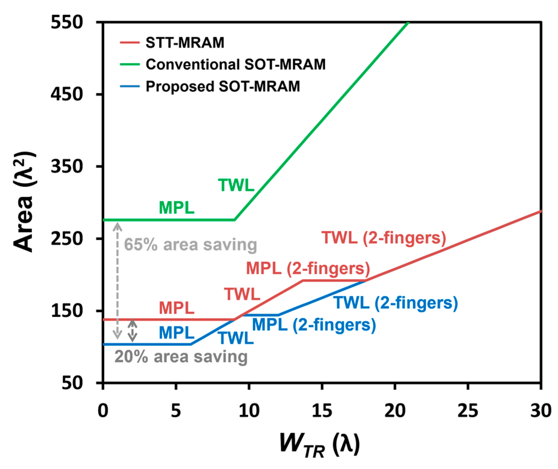
Figure 7 compares the area of STT-MRAM, conventional SOT-MRAM, and the proposed MRAM according to the transistor width. The proposed ultra-high-density version of SOT-MRAM displays an area savings of 65% over conventional SOT-MRAM in the MPL region. Even compared to STT-MRAM, the area in the MPL area is 25% smaller using the horizontal dimension reduction technique. Unlike conventional SOT-MRAM, the proposed memory can further optimize the area using a fingered transistor if the transistor width exceeds 9.5λ. Therefore, when the larger size of the transistor is required for design specification, the greater the area efficiency can be achieved compared to conventional SOT-MRAM by using a two-finger transistor.
4. Simulations and Results
To evaluate the effectiveness of the proposed memory design for comparison with STT-MRAM and conventional SOT-MRAM, we employed a simulation framework [31] encompassing four components:
- The simulation program integrated circuit emphasis (SPICE) simulator modeled the MRAM bit-cells.
The Landau–Lifshitz–Gilbert equation solver calculates the critical current required for a switching time of 10 ns using the parameters in Table 1. For the SOT device, the efficiency of the spin current injection, represented as the ratio of IS to IC, can be obtained using the formula [16,25]:
where AMTJ refers to the cross-sectional area of the MTJ in the xy-plane, AHM denotes the cross-sectional area of the HM in the yz-plane, tHM signifies the thickness of the HM, λsf represents the spin-flip length, and θSH denotes a spin Hall angle, which we set to 0.3 in the analysis [17]. As AHM (= WHM × tHM) is set smaller than AMTJ (= π/4 × WFL × LFL), the resulting spin current injection efficiency achieves 254%, enabling low current write operation.
The resistance characteristics of the HM are acquired from experimental resistivity data found in [17]. Meanwhile, the voltage-dependent resistance of the MTJ is derived using the nonequilibrium Green’s function formalism, as explained in [10,34]. Additionally, we emulate the behavior of the diode by employing a Verilog-A compact model, where we have successfully calibrated the voltage-dependent current values to match experimental results from a TiOX-based Schottky diode with a cross-sectional area of 4µm2 [28]. To estimate the current flow for the proposed device dimensions (an elliptical shape of 120 × 40 nm), we extrapolate the current density trends observed in experiments with varying cross-sectional areas [22].
By integrating the resistance characteristics of the spintronic device and the model compatible with the SPICE simulator of the Schottky diode with a commercial 45 nm transistor, we conducted transient circuit simulations to evaluate the three distinct memory bit-cells. The design of the three memory bit-cells was executed under identical conditions, including a 10-ns switching time, a 10% write margin (defined as (IW − IC)/IC, where IW represents the write current and IC signifies the critical current), and a read-disturb margin of >50% (defined as (IC − IR)/IC, with IR representing the read current) [5].
Table 2 presents the simulation results. For STT-MRAM, where the paths for both the write and read currents are identical, the size of the access transistor is determined to accommodate write and read operations. The transistor width is 380 nm in the analysis, primarily based on write operation requirements rather than read operations. Owing to its high spin current injection efficiency, the smaller transistor width of 120 nm is sufficient to achieve the same write operation conditions for SOT-MRAM. However, due to the need for an additional transistor for the read, the bit-cell area of conventional SOT-MRAM (0.1104 µm2) is 20% larger than that of STT-MRAM (0.0880 µm2).
In contrast, the proposed SOT-MRAM can mitigate the problem of a longer vertical dimension overhead by replacing the read transistor with the Schottky diode. Moreover, the proposed memory shares an SL between two neighboring memory cells in the same row, resulting in a smaller horizontal dimension than conventional memory. Therefore, the proposed high-density memory cell achieves a 48% smaller area than STT-MRAM.
Importantly, the proposed design preserves the inherent advantages of SOT-MRAM. Thanks to its remarkable spin current injection efficiency, which stands at 254%, our proposed MRAM design reduces write power significantly by 68% when compared to STT-MRAM. Furthermore, unlike STT-MRAM, where the oxide thickness (tMgO) is constrained by the trade-off between writability and read stability, our proposed design allows the optimization of tMgO exclusively for read operations. This advantage stems from the fact that the oxide layer does not play a role in the write current path. Consequently, employing a thicker oxide layer becomes feasible, enhancing the read-disturb margin by 1.9× with a 29% improvement in read power. Nevertheless, the proposed MRAM exhibits a higher read power consumption than conventional SOT-MRAM due to the necessity of raising the read voltage to surpass the diode turn-on voltage.
5. Conclusions
This paper proposes an ultra-high-density SOT-MRAM design. Using a diode on the read current path instead of a read access transistor, SOT-MRAM can be a single-transistor-based design such that the vertical dimension can be reduced by up to 50%. Moreover, by combining the SL of two adjacent cells in the same row, a horizontal dimension reduction also can be achieved by up to 25%. The proposed memory cell preserves the benefits of conventional SOT-MRAM, including enhanced reliability and reduced write power. Simulation results reveal that the proposed design technique reduces the bit-cell size by 63% and 48%, compared with STT-MRAM and conventional SOT-MRAM, respectively. In comparison to STT-MRAM, the proposed configuration yields a substantial 68% reduction in write power, a 29% decrease in read power, and a 1.9× improved read-disturb margin.
Author Contributions
Conceptualization, Y.S.; Methodology, Y.S. and K.-W.K.; Validation, Y.S. and K.-W.K.; Formal analysis, Y.S. and K.-W.K.; Investigation, Y.S. and K.-W.K.; Resources, Y.S. and K.-W.K.; Data curation, Y.S.; Writing—original draft, Y.S. and K.-W.K.; Writing—review & editing, Y.S. and K.-W.K.; Visualization, Y.S. and K.-W.K.; Supervision, Y.S. and K.-W.K.; Project administration, Y.S. and K.-W.K.; Funding acquisition, Y.S. All authors have read and agreed to the published version of the manuscript.
Funding
This work was supported by the INHA UNIVERSITY Research Grant.
Data Availability Statement
All data that support the findings of this study are included within the article.
Conflicts of Interest
The authors declare no conflict of interest.
References
- Li, Y.; Kang, W.; Zhou, K.; Qiu, K.; Zhao, W. Experimental Demonstration of STT-MRAM-based Nonvolatile Instantly On/Off System for IoT Applications: Case Studies. ACM Trans. Embed. Comput. Syst. 2023, 22, 1–24. [Google Scholar] [CrossRef]
- Yazigy, N.; Postel-Pellerin, J.; Della Marca, V.; Terziyan, K.; Sousa, R.C.; Canet, P.; Di Pendina, G. Real-Time Switching Dynamics in STT-MRAM. IEEE J. Electron Devices Soc. 2022, 10, 490–494. [Google Scholar] [CrossRef]
- Chun, K.C.; Zhao, H.; Harms, J.D.; Kim, T.-H.; Wang, J.-P.; Kim, C.H. A scaling roadmap and performance evaluation of in-plane and perpendicular mtj based stt-mrams for high-density cache memory. IEEE J. Solid-State Circuits 2013, 48, 598–610. [Google Scholar] [CrossRef]
- Augustine, C.; Mojumder, N.; Fong, X.; Choday, H.; Park, S.P.; Roy, K. STT-MRAMs for future universal memories: Perspective and prospective. In Proceedings of the 2012 28th International Conference on Microelectronics Proceedings, Nis, Serbia, 13–16 May 2012; pp. 349–355. [Google Scholar] [CrossRef]
- Seo, Y.; Kwon, K.-W. Area Optimization Techniques for High-Density Spin-Orbit Torque MRAMs. Electronics 2021, 10, 792. [Google Scholar] [CrossRef]
- Wang, C.-Y.; Shih, M.-C.; Weng, C.-H.; Chen, C.-H.; Chang, C.-Y.; Wang, W.; Chiang, T.W.; Hung, A.; Chuang, H.; Gallagher, W.J. Reliability demonstration of reflow qualified 22 nm stt-mram for embedded memory applications. In Proceedings of the 2020 IEEE Symposium on VLSI Technology, Honolulu, HI, USA, 16–19 June 2020; p. TM3.2. [Google Scholar] [CrossRef]
- Li, J.; Ndai, P.; Goel, A.; Salahuddin, S.; Roy, K. Design Paradigm for Robust Spin-Torque Transfer Magnetic RAM (STT MRAM) From Circuit/Architecture Perspective. IEEE Trans. Very Large Scale Integr. (VLSI) Syst. 2009, 18, 1710–1723. [Google Scholar] [CrossRef]
- Sun, G.; Dong, X.; Xie, Y.; Li, J.; Chen, Y. A novel architecture of the 3D stacked MRAM L2 cache for CMPs. In Proceedings of the 2009 IEEE 15th International Symposium on High Performance Computer Architecture, Raleigh, NC, USA, 14–18 February 2009; pp. 239–249. [Google Scholar]
- Fong, X.; Kim, Y.; Choday, S.H.; Roy, K. Failure Mitigation Techniques for 1T-1MTJ Spin-Transfer Torque MRAM Bit-cells. IEEE Trans. Very Large Scale Integr. (VLSI) Syst. 2014, 22, 384–395. [Google Scholar] [CrossRef]
- Lin, C.; Kang, S.; Wang, Y.; Lee, K.; Zhu, X.; Li, X.; Hsu, W.; Kao, Y.; Liu, M.; Chen, W.; et al. 45nm low power CMOS logic compatible embedded STT MRAM utilizing a reverse-connection 1T/1MTJ cell. In Proceedings of the IEEE International Electron Devices Meeting, Baltimore, MD, USA, 7–9 December 2009; pp. 11.6.1–11.6.4. [Google Scholar] [CrossRef]
- Seo, Y.; Kwon, K.-W.; Fong, X.; Roy, K. High Performance and Energy-Efficient On-Chip Cache Using Dual Port (1R/1W) Spin-Orbit Torque MRAM. IEEE J. Emerg. Sel. Top. Circuits Syst. 2016, 6, 293–304. [Google Scholar] [CrossRef]
- Cai, K.; Talmelli, G.; Fan, K.; Van Beek, S.; Kateel, V.; Gupta, M.; Monteiro, M.; Ben Chroud, M.; Jayakumar, G.; Trovato, A.; et al. First demonstration of field-free perpendicular SOT-MRAM for ultrafast and high-density embedded memories. In Proceedings of the 2022 International Electron Devices Meeting (IEDM), San Francisco, CA, USA, 3–7 December 2022; pp. 36.2.1–36.2.4. [Google Scholar] [CrossRef]
- Song, M.Y.; Lee, C.M.; Yang, S.Y.; Chen, G.L.; Chen, K.M.; Wang, I.J.; Hsin, Y.C.; Chang, K.T.; Hsu, C.F.; Lin, S.J. High speed (1ns) and low voltage (1.5V) demonstration of 8Kb SOT-MRAM array. In Proceedings of the IEEE Symposium on VLSI Technology and Circuits, Honolulu, HI, USA, 12–17 June 2022; pp. 377–378. [Google Scholar] [CrossRef]
- Kim, T.; Jang, Y.; Kang, M.-G.; Park, B.-G.; Lee, K.-J.; Park, J. SOT-MRAM Digital PIM Architecture With Extended Parallelism in Matrix Multiplication. IEEE Trans. Comput. 2022, 71, 2816–2828. [Google Scholar] [CrossRef]
- Seo, Y.; Kwon, K.-W. Area-optimized design of SOT-MRAM. IEICE Electron. Express 2020, 17, 20200314. [Google Scholar] [CrossRef]
- Manipatruni, S.; Nikonov, D.E.; Young, I.A. Voltage and Energy-Delay Performance of Giant Spin Hall Effect Switching for Magnetic Memory and Logic. arXiv 2013, arXiv:1301.5374. [Google Scholar]
- Pai, C.-F.; Liu, L.; Li, Y.; Tseng, H.W.; Ralph, D.C.; Buhrman, R.A. Spin transfer torque devices utilizing the giant spin Hall effect of tungsten. Appl. Phys. Lett. 2012, 101, 122404. [Google Scholar] [CrossRef]
- Liu, L.; Pai, C.-F.; Li, Y.; Tseng, H.W.; Ralph, D.C.; Buhrman, R.A. Spin-Torque Switching with the Giant Spin Hall Effect of Tantalum. Science 2012, 336, 555–558. [Google Scholar] [CrossRef] [PubMed]
- Cai, K.; Van Beek, S.; Rao, S.; Fan, K.; Gupta, M.; Nguyen, V.D.; Jayakumar, G.; Talmelli, G.; Couet, S.; Kar, G.S. Selective operations of multi-pillar SOT-MRAM for high density and low power embedded memories. In Proceedings of the IEEE Symposium on VLSI Technology and Circuits, Honolulu, HI, USA, 12–17 June 2022; pp. 375–376. [Google Scholar] [CrossRef]
- Endoh, T.; Honjo, H.; Nishioka, K.; Ikeda, S. Recent Progresses in STT-MRAM and SOT-MRAM for Next Generation MRAM. In Proceedings of the 2020 IEEE Symposium on VLSI Technology, Honolulu, HI, USA, 16–19 June 2020; p. TMFS.1. [Google Scholar] [CrossRef]
- Natsui, M.; Tamakoshi, A.; Honjo, H.; Watanabe, T.; Nasuno, T.; Zhang, C.; Tanigawa, T.; Inoue, H.; Niwa, M.; Yoshiduka, T.; et al. Dual-Port SOT-MRAM Achieving 90-MHz Read and 60-MHz Write Operations Under Field-Assistance-Free Condition. IEEE J. Solid-State Circuits 2021, 56, 1116–1128. [Google Scholar] [CrossRef]
- Seo, Y.; Kwon, K.-W.; Roy, K. Area-Efficient SOT-MRAM With a Schottky Diode. IEEE Electron Device Lett. 2016, 37, 982–985. [Google Scholar] [CrossRef]
- Jang, Y.; Park, J. Area and energy efficient joint 2T SOT-MRAM-based on diffusion region sharing with adjacent cells. IEEE Trans. Circuits Syst. II Express Briefs 2022, 69, 1622–1626. [Google Scholar] [CrossRef]
- Hoffmann, A. Spin Hall effects in metals. IEEE Trans. Magn. 2013, 49, 5172–5193. [Google Scholar] [CrossRef]
- Kim, Y.; Fong, X.; Kwon, K.-W.; Chen, M.-C.; Roy, K. Multilevel Spin-Orbit Torque MRAMs. IEEE Trans. Electron Devices 2014, 62, 561–568. [Google Scholar] [CrossRef]
- Gupta, S.K.; Park, S.P.; Mojumder, N.N.; Roy, K. Layout-aware optimization of stt mrams. In Proceedings of the Design, Automation & Test in Europe Conference & Exhibition, Dresden, Germany, 12–16 March 2012; pp. 1455–1458. [Google Scholar] [CrossRef]
- Liebmann, L. DfM, the teenage years. In Proceedings of the SPIE Advanced Lithography, San Jose, CA, USA, 24–29 February 2008; Volume 6925, p. 692502. [Google Scholar] [CrossRef]
- Li, Y.T.; Long, S.B.; Lv, H.B.; Liu, Q.; Wang, M.; Xie, H.W.; Zhang, K.W.; Yang, X.Y.; Liu, M. Novel self-compliance Bipolar 1D1R memory device for high-density RRAM application. In Proceedings of the 2013 5th IEEE International Memory Workshop, Monterey, CA, USA, 26–29 May 2013; pp. 184–187. [Google Scholar] [CrossRef]
- Nayak, D.; Acharya, D.P.; Rout, P.K.; Nanda, U. A high stable 8T-SRAM with bit interleaving capability for minimization of soft error rate. Microelectron. J. 2018, 73, 43–51. [Google Scholar] [CrossRef]
- Shi, Y.Q.; Zhang, X.M.; Ni, Z.-C.; Ansari, N. Interleaving for combating bursts of errors. IEEE Circuits Syst. Mag. 2004, 4, 29–42. [Google Scholar] [CrossRef]
- Fong, X.; Gupta, S.K.; Mojumder, N.N.; Choday, S.H.; Augustine, C.; Roy, K. KNACK: A hybrid spin-charge mixed-mode simulator for evaluating different genres of spin-transfer torque MRAM bit-cells. In Proceedings of the International Conference on Simulation of Semiconductor Processes and Devices, Osaka, Japan, 8–10 September 2011; pp. 51–54. [Google Scholar] [CrossRef]
- Slonczewski, J.C. Current-driven excitation of magnetic multilayers. J. Magn. Magn. Mater. 1996, 159, L1–L7. [Google Scholar] [CrossRef]
- Gilbert, T. A phenomenological theory of damping in ferromagnetic materials. IEEE Trans. Magn. 2004, 40, 3443–3449. [Google Scholar] [CrossRef]
- Datta, D.; Behin-Aein, B.; Salahuddin, S.; Datta, S. Quantitative model for TMR and spin-transfer torque in MTJ devices. In Proceedings of the International Electron Devices Meeting, San Francisco, CA, USA, 6–8 December 2010; pp. 22.8.1–22.8.4. [Google Scholar] [CrossRef]
Figure 1.
(a) Device structure and resistance states of magnetic tunnel junction, (b) current paths for write and read operation of the STT-MRAM cell, (c) probability of read-disturb failure and probability of write failure with respect to the range of the access transistor width [5].
Figure 1.
(a) Device structure and resistance states of magnetic tunnel junction, (b) current paths for write and read operation of the STT-MRAM cell, (c) probability of read-disturb failure and probability of write failure with respect to the range of the access transistor width [5].

Figure 2.
(a) Device structure of Spin obit torque (SOT), and example of switching ‘0’ operation, (b) SOT-MRAM cell schematic, and write and read current direction, (c) biasing condition for write and read operations.
Figure 2.
(a) Device structure of Spin obit torque (SOT), and example of switching ‘0’ operation, (b) SOT-MRAM cell schematic, and write and read current direction, (c) biasing condition for write and read operations.

Figure 3.
(a) Parameters and its value of our assumed layout design rules, (b) conventional SOT-MRAM layout in metal pitch limited (MPL) (max(WTR-R, WTR-W) < 9λ). (c) conventional SOT-MRAM layout in transistor width limited (TWL) (max(WTR-R, WTR-W) > 9λ).
Figure 3.
(a) Parameters and its value of our assumed layout design rules, (b) conventional SOT-MRAM layout in metal pitch limited (MPL) (max(WTR-R, WTR-W) < 9λ). (c) conventional SOT-MRAM layout in transistor width limited (TWL) (max(WTR-R, WTR-W) > 9λ).

Figure 4.
Schematic and layout of (a) conventional SOT-MRAM, (b) SOT-MRAM with the vertical dimension reduction technique, and (c) SOT-MRAM with the vertical and horizontal dimension reduction technique.
Figure 4.
Schematic and layout of (a) conventional SOT-MRAM, (b) SOT-MRAM with the vertical dimension reduction technique, and (c) SOT-MRAM with the vertical and horizontal dimension reduction technique.

Figure 5.
(a) Biasing conditions of the SOT-MRAM, (b) odd-column cell write operation of SOT-MRAM in two-bit interleaved architecture, (c) even-column cell read operation of SOT-MRAM in two-bit interleaved architecture.
Figure 5.
(a) Biasing conditions of the SOT-MRAM, (b) odd-column cell write operation of SOT-MRAM in two-bit interleaved architecture, (c) even-column cell read operation of SOT-MRAM in two-bit interleaved architecture.

Figure 6.
Proposed SOT-MRAM layouts with a single-finger transistor (a) when WTR is smaller than 6λ, (b) when WTR is larger than 6λ, and proposed SOT-MRAM layouts with a two-finger transistor (c) when WTR is smaller than 12λ, (d) when WTR is larger than 12λ.
Figure 6.
Proposed SOT-MRAM layouts with a single-finger transistor (a) when WTR is smaller than 6λ, (b) when WTR is larger than 6λ, and proposed SOT-MRAM layouts with a two-finger transistor (c) when WTR is smaller than 12λ, (d) when WTR is larger than 12λ.
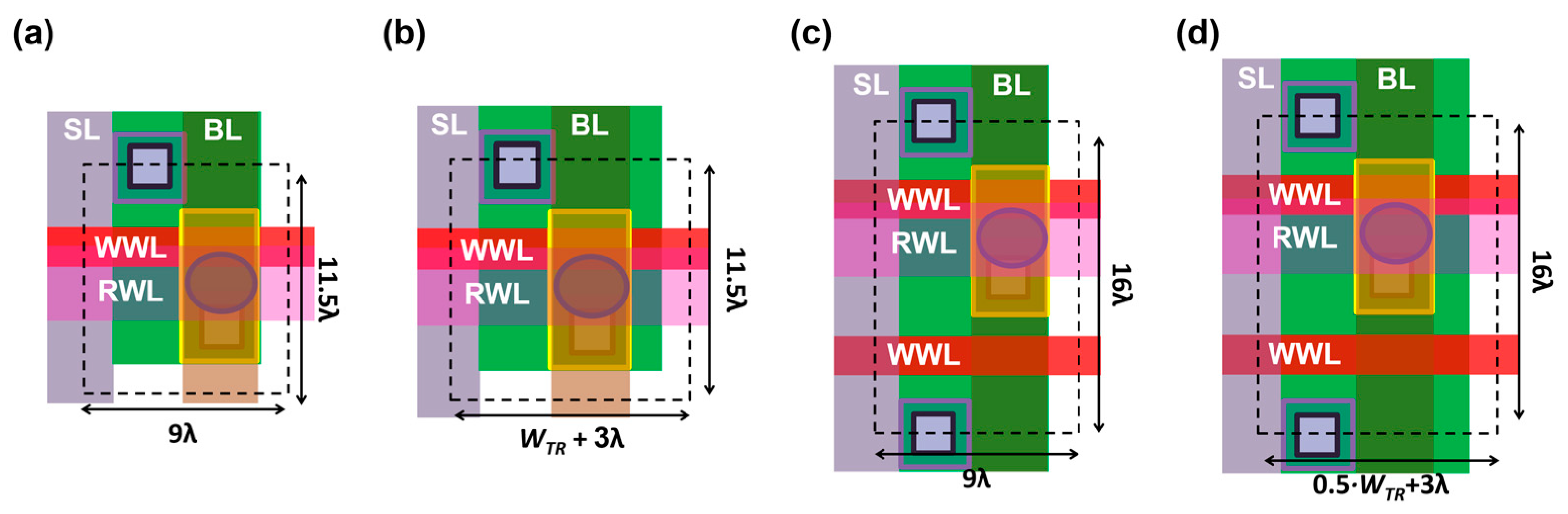
Figure 7.
Memory cell area comparison of STT-MRAM, conventional SOT-MRAM, and the proposed SOT-MRAM. MRAM cell area is limited by metal pitch (MPL) or transistor width (TWL).
Figure 7.
Memory cell area comparison of STT-MRAM, conventional SOT-MRAM, and the proposed SOT-MRAM. MRAM cell area is limited by metal pitch (MPL) or transistor width (TWL).

Table 1.
Parameters for spintronic devices.
| Device Parameters | STT Device | SOT Device |
|---|---|---|
| Gilbert damping, α | 0.007 | 0.0122 |
| Saturation magnetization, MS | 1000 × 103 A/m | 1000 × 103 A/m |
| FL dimension (WFL × LFL × tFL) | 120 × 40 × 2 nm a | 120 × 40 × 2 nm a |
| HM dimension (WHM × LHM × tHM) | - | 120 × 80 × 2.5 nm |
| HM resistivity | - | 200 µΩ·cm |
| Spin hall angle, θSH | - | 0.3 |
| Spin flip length, λsf | - | 1.40 nm |
| MgO thickness, tMgO | 1.15 nm | 1.40 nm |
| Critical current for 10-ns switching time | 139 µA | 87 µA |
a The FL of MTJ is elliptical. (FL: free layer, HM: heavy metal, STT: spin-transfer torque, SOT: spin-orbit torque.
Table 2.
Comparison of three different memory cells in terms of area, write and read power, and read-disturb margin.
Table 2.
Comparison of three different memory cells in terms of area, write and read power, and read-disturb margin.
| STT-MRAM | Conventional SOT-MRAM | Proposed SOT-MRAM | |
|---|---|---|---|
| Transistor width (nm) | 380 | 120 (WTR-R) 120 (WTR-W) | 120 |
| Bit-cell area (µm2) | 0.0800 | 0.1104 | 0.0414 |
| VWRITE (V) | 1.0 | 0.6 | 0.6 |
| VREAD (V) | 0.2 | 0.2 | 0.8 |
| Write power (µW) | 193.48 | 61.08 | 61.07 |
| Read power (µW) | 10.14 | 1.84 | 7.21 |
| Read-disturb margin (%) | 51 | 94 | 95 |
Disclaimer/Publisher’s Note: The statements, opinions and data contained in all publications are solely those of the individual author(s) and contributor(s) and not of MDPI and/or the editor(s). MDPI and/or the editor(s) disclaim responsibility for any injury to people or property resulting from any ideas, methods, instructions or products referred to in the content. |
© 2023 by the authors. Licensee MDPI, Basel, Switzerland. This article is an open access article distributed under the terms and conditions of the Creative Commons Attribution (CC BY) license (https://creativecommons.org/licenses/by/4.0/).
Share and Cite
MDPI and ACS Style
Seo, Y.; Kwon, K.-W. Ultra High-Density SOT-MRAM Design for Last-Level On-Chip Cache Application. Electronics 2023, 12, 4223. https://doi.org/10.3390/electronics12204223
AMA Style
Seo Y, Kwon K-W. Ultra High-Density SOT-MRAM Design for Last-Level On-Chip Cache Application. Electronics. 2023; 12(20):4223. https://doi.org/10.3390/electronics12204223
Chicago/Turabian StyleSeo, Yeongkyo, and Kon-Woo Kwon. 2023. "Ultra High-Density SOT-MRAM Design for Last-Level On-Chip Cache Application" Electronics 12, no. 20: 4223. https://doi.org/10.3390/electronics12204223
Note that from the first issue of 2016, this journal uses article numbers instead of page numbers. See further details here.