
Graded Bandgap Ultrathin CIGS Solar Cells

1
Electronics and Communication Engineering Department, Kuwait College of Science and Technology, Road N. 7, Doha 13113, Kuwait
2
Department of Mathematics and Computer Science, Physics and Earth Science (MIFT), University of Messina, Viale F. Stagno d’Alcontres 31, 98166 Messina, Italy
3
Electrical Engineering Department, University of Abd-Elhamid Ibn Badis, Bp227, Mostaganem 27000, Algeria
4
BIOMORF Department, University of Messina, 98125 Messina, Italy
*
Author to whom correspondence should be addressed.
Electronics 2023, 12(2), 393; https://doi.org/10.3390/electronics12020393
Submission received: 18 December 2022
/
Revised: 11 January 2023
/
Accepted: 11 January 2023
/
Published: 12 January 2023
(This article belongs to the Special Issue Power Electronics for Renewable Energy Systems: Latest Advances and Prospects)
Abstract
:In this paper, we physically modeled passivated ultrathin Cu (In1−xGax) Se2 solar cells with different bandgap grading configurations. Firstly, we have designed the cell architecture according to the fabricated model. The novelty in this work is the modeling of passivated u-CIGS solar cells with different bandgap grading profile configurations in order to achieve high efficiency with a thickness of 500 nm. A significant influence on device performance has been observed while changing absorber doping density, electron affinity, and operating temperature (range of 10–70 °C) for the investigated samples. ZnS has been used as a buffer layer to replace the conventional CdS material in order to improve cell efficiency. The impact of the buffer doping density and electron affinity on u-CIGS cell performance is explored. The simulation results show that a high bandgap at the front and rear sides with an acceptor density of 2 × 10¹⁶ provide the best electrical cell parameters: Jsc of 31.53 mA/cm2, Voc of 742.78 mV, FF of 77.50%, η of 18.15%. Our findings can be considered guidelines for new single and/or tandem cell optimization to achieve high efficiency.
1. Introduction
Thin-film (TF) PV technology has significantly developed, and among all TF PV technologies, CIGS-based solar cells have the highest cell and module efficiencies [1,2]. These types of solar cells are still competing with silicon PV technology which dominates 95% of the PV market due to their environmentally friendly nature, long-term durability, and low fabrication costs [1,2,3]. The main advantage of TF PV is flexibility by reducing the substrate weight and rigidity, which represents a potential to reduce manufacturing costs [3,4,5]. For the ultrathin-film Cu (In1−xGax) Se2 solar cells, reducing the thickness of the absorber is advantageous due to decreasing the amount of indium (In) and gallium (Ga), which are critical raw materials. However, reducing absorber thickness causes insufficient photon absorption rate and the detrimental impact of back-surface recombination, resulting in a degradation in cell efficiency [5,6,7]. Many approaches have been addressed to keep or improve the power conversion efficiency while the absorber layers are thinner [7,8,9,10,11,12,13,14,15]. First, bandgap grading by changing the Ga content in the absorber is considered a traditional way to improve Voc for a thinner absorber layer [15,16,17,18,19,20,21,22,23,24,25,26]. Many research works have delighted the positive impact of bandgap grading profiles in the generation and collection of minority carriers [26,27,28,29,30,31,32,33,34]. It has been found that double grading allows benefiting from the advantages of both high grading at the front and back side of the cell [30,34]. However, Ga grading is not a complete solution for passivation and rear recombination [1,8]. Consequently, new approaches have been sought to passivate the rear surface of u-CIGS [1,10]. Initiating a passivation layer using Al2O3 material with an opening of physical contact between the absorber and the rear contact is one of the solutions to this problem [1,8]. The rear passivation of ultrathin-film Cu (In1−xGax) Se2 solar cells have attracted much attention in recent years due to their outstanding photovoltaic performance [1,2,3,4,5,6,7,8,9,10]. Furthermore, due to their tunable bandgap, they could be integrated into tandem cell configurations as better top and/or bottom cells [8,27].
In this paper, three different devices are analyzed correlating cells’ performance on the absorber bandgap grading profile and describing pathways to obtain an efficient cell. Firstly, we have designed the cell architecture according to the fabricated model reported by Jackson et al. [1]. Then, it is very necessary to investigate the effect of the graded bandgap, electron affinity, absorber doping density, and operating temperature on cell performance. The conventional buffer layer of CdS is nearly optimum for CIGS with a smaller bandgap ranging from 1 to 1.35 eV but shows poor alignment for a higher Ga ratio CIGS absorber with a higher bandgap [29,30,31,32,33,34]. The CdS possesses a low bandgap of 2.4 eV, which is not sufficient to cover the maximum shorter wavelength of photons, resulting in absorption losses. For high efficiency, it is necessary to replace the CdS buffer layer (BL), which still contains the toxic Cd, with better suited BL to form a good heterojunction [33,34,35,36]. Introducing ZnS as a better n-type BL due to its high-bandgap semiconducting and better lattice match with CIGS [34,35,36,37,38,39,40], it has been found that using dielectric passivation layers at the front could increase light absorption and be sufficient to establish long-term stability [34,35]. Up to date, no improvements have been observed for solar cells based on absorber/passivation structures [34,35,36]. In the last part, we analyzed the positive impact of ZnS as the buffer layer and MgF2 as the ARC layer on optimized samples.
2. Device Architecture
Figure 1 represents the structure of an ultrathin CIGS solar cell designed in this work using the Silvaco TCAD software package. The investigated cell was designed according to the fabricated structure reported by Jackson et al. [1]. The cell consists of a conventional n-i-n-p structure. The cell layers are ZnO:Al/ZnO/CdS/u-CIGS/Al2O3/Mo/glass-substrate from bottom to top. Herein, CIGS is used as a photo-absorbing layer, whereas ZnO:Al and CdS are used as window and buffer layers, respectively. According to reference [1], a 500 nm-thick CIGS absorber layer is considered; ZnO:Al, ZnO, and CdS thickness are set 300 nm, 100 nm, and 50 nm, respectively. The advantage of reducing the thickness of the absorber layer leads to minimizing the bulk defects, thereby improving overall recombination losses [1]. Aluminum oxide (Al2O3, 25 nm-thick) has been used for the rear passivation. This part has been investigated accordingly in detail in our previous research work [2,10,23]. Schottky (4.7 eV) and ohmic contact were assumed for the front and rear electrodes, respectively [1,2,3]. Experimentally, during the growth of the CIGS absorber on the metal molybdenum substrate, a thin interface layer of MoSe2 is formed, resulting in a quasi-ohmic contact, which is the reason for using molybdenum as a back contact [3]. Table 1 illustrates device parameters for a passivated u-CIGS solar cell model [1].
3. Device Validation
For device simulation, the FLDMOB, CONMOB, BGN, SRH, CONSRH, and Auger recombination were included in the program. Fermi–Dirac distribution has been enabled. For interface defects, the trap-assisted tunneling model was also considered [28]. Initially, the investigated 2D passivated u-CIGS solar cell model was carefully calibrated according to the fabricated cell [1]. Along the calibration, some physical parameters such as the defect densities and interface trap densities were carefully adjusted. To emulate the series resistance (Rs), the rear contact resistance (Rc = 0.181 Ω.cm2) has been used. A surface recombination velocity (SRV) of 102 cm/s was considered on the rear side between the absorber (CIGS) and a passivation layer (Al2O3) [1,2]. Figure 2 illustrates the simulated current–voltage, power–voltage, quantum efficiency (QE), and integrated current density characteristics under AM1.5 illumination. Table 2 illustrates a comparison between the simulated and measured cell parameters. Further, the studied cell model was also compared to our recent work [2].
4. Results and Discussion
Initially, we studied different ways for bandgap grading profiles to enhance the ultrathin CIGS-based solar cells’ efficiency. Bandgap grading profile configuration was considered this recent decade to be a very promising approach to obtain high efficiency. Apart from the absorber bandgap grading study, the electron affinity and doping density of the majority carriers in the absorber layer were also analysed for their effect on photovoltaic cell device performance. The investigated solar cell model has a 2D design configuration as shown in Figure 1. The numerical simulation of the investigated cell models was evaluated at a room temperature of 300 K.
4.1. Impact of Graded Bandgap of the Absorber Layer
The CIGS absorber plays a significant role in the photovoltaic parameters by the absorber layer thickness and Ga-composition grading profile [6]. The bandgap energy Eg of the absorber layer is dependent on the composition ratio x = Ga/(In + Ga). For high efficiency, we investigate the absorber composition for single and double bandgap grading across the absorber layer by increasing Ga toward the front and back on cell performance [29]. Generally, generated carriers (electrons) within the space charge region (SCR) are efficiently collected by front contact, owing to the presence of a strong electric field at the heterointerface. However, at the forward bias operation, significantly SCR width declines, and high Ga content at the front surface can result from a barrier for electrons. This barrier will not have a strong effect on minority carriers due to thermal energy that would be sufficient for most of the electrons to overcome it. Figure 3 illustrates the band diagram of the investigated u-CIGS solar cell for two different absorber bandgap configurations under zero-bias voltage conditions. Reducing interface recombination at the front and back has resulted while increasing the Ga content at the absorber sides. Front and rear recombination are mainly lessened by the presence of a buffer layer and a passivated Al2O3 layer, respectively. The Al2O3 passivation with a negative fixed charge implemented exhibits better rear surface passivation and low interfacial charge recombination [2]. Figure 4 illustrates the electron concentration and recombination rate in the u-CIGS solar cells for three different absorber bandgap configurations. In the absorber layer, nonradiative recombination near the heterointerface causes a reduction in Voc. Increasing the energy bandgap towards the front surface of the absorber layer would improve Voc, thus preventing voltage losses; see Figure 3a and Figure 4. Increasing the energy bandgap towards the rear surface of the absorber layer would reduce the rear recombination at the CIGS/Mo interface enhancing Jsc; see Figure 3b and Figure 4. The current density of the cell with graded bandgap in upward (high Ga content in the rear side) configuration is 29.12 mA/cm2 under AM 1.5 G with a light intensity of 100 mW/cm2, which results in photovoltaic cell efficiency of 13.54% in the hot electron device cell. Compared with that of the graded bandgap in a downward (high Ga content in the front side) configuration (21.72 mA/cm2), the cell exhibited an increase in efficiency of 13.45%. This could be acting as a source of increasing recombination, mainly reducing Jsc and FF, thus resulting in low conversion efficiencies. The Jsc under AM 1.5 G improved on the single structure when the bandgap is increasing toward the back-surface side; however, the fill factor (FF) increased because the resistance factors of the cell decreased. It is worth presenting here in this paper that this study covers the challenges and limits related to the absorber layer and possible pathways to enhancing cell efficiency.
In this simulation work, the double-grading of the absorber bandgap was implemented by increasing Ga content toward the front and rear surface, which can act as an efficient barrier for electrons, thus preventing the front and rear recombination, enhancing Jsc and Voc [6]. Figure 5 illustrates the band diagram of the investigated u-CIGS solar cell for two different absorber bandgap configurations under zero-bias voltage conditions. The variation in photovoltaic parameters on the absorber-layer bandgap grading is tabulated in Table 3. Figure 5 also illustrates a comparison of the J–V curves of the investigated u-CIGS models. Large values of Jsc and Voc were obtained (~29.16 mA/cm2 and ~748.778 mV) with the investigated bandgap grading mainly due to less rear and front carrier recombination, respectively. Heretofore, the results show that double grading causes only positive effects on cell performance (Jsc and Voc). However, let us recall that the physical properties of the absorber layer are assumed to be uniform (carrier lifetimes and mobilities, etc.). In practice, it is reasonable that increasing Ga content in the absorber layer lowers material quality by increasing point defects and dislocations; lowering grain size; and defect levels appearing in the bandgap, among other effects [30,31].
4.2. Impact of Varying Electron Affinities of the Absorber Layer
Absorber affinity has a high level of achieving a good conversion rate according to the literature [23]. As a result, we executed a Silvaco simulation to investigate how the affinity of the absorber (4.3–4.65) affects the device’s performance. Figure 6 shows the variation of the PV characteristics with respect to the electron affinity of the absorber layer. It is observed that Jsc remains constant with electron affinity for the three samples. Voc falls off smoothly while increasing electron affinity due to the recombination of the free charge carriers at the heterointerface. It shows a strong effect on the sample with downward grading (green) due to back recombination. It is seen that the PCEs of the two devices (red and blue) are low with low electron affinity. The moderate value of absorber affinity like 4.45–4.65 eV provides a moderately high and stable PCE for the device’s configuration under study. This enhancement is due to the increase in the FF of the device. However, for a device with a graded bandgap in a downward configuration (Green), it is seen that the efficiency enhanced with a low electron affinity of more than 16.5%. The material parameters of the absorber layer were optimized for achieving the maximum possible efficiency from the results of numerical simulation.
4.3. Impact of Varying Acceptor Doping Concentration of the Absorber Layer
Figure 7 shows simulated cell characteristic contours as a function of the absorber doping density under the AM1.5G spectrum. Three different cell samples were considered for this study: u-CIGS with a bandgap in upward, downward, and doubled grading configurations. The doping density in the absorber layer varied from 1014 to 1018 cm−3. Generally, a thick absorber is not suitable as it causes high recombination for photogenerated carriers [2]. Similarly, there were no benefits from a high doping level in the absorber, as poor photon absorption entails lower η values, such as in the case of a cell with an upward bandgap grading configuration [2]. From Figure 7, doping variation has a strong effect on one sample with a graded bandgap in an upward configuration (blue) compared to other investigated samples (green and red). A decrease in Jsc is observed after 1016 cm−3 due to an increase in effective recombination in the absorber layer. Voc follows the opposite trend with doping densities due to a decrease in the Fermi energy level of the holes and also because of the elevation of charge separation. For the blue sample, the high doping in the CIGS absorber is not beneficial for the generated carriers, thus reducing the Jsc but increasing the Voc at the same time. Therefore, the PCE of the sample (blue) is determined by a compromise between the Jsc and Voc. The optimal doping level for a 0.5 μm-thick CIGS layer gradually shifts between 2 × 1016 cm−3 and 5 × 1016 cm−3. The optimum PEC that can be extracted is around 13.5%. These results are in agreement with the literature [1,2,3,4,5], which showed that a single u-CIGS solar cell does not require high doping concentration for the absorber layer to achieve high efficiency.
4.4. Temperature Dependence
The simulations have demonstrated that it is important to reevaluate the suitable CIGS absorber layer in terms of bandgap grading configuration and doping density. Herein, we carried out an important study about the effect of operating temperature on investigated samples in the temperature range of 10–70 °C [41]. Generally, the standard operating temperature for investigated three samples is taken at 25 °C. Nevertheless, during device operation, the cell is subjected to a high operating temperature. Degradation in cell parameters such as Jsc, Voc, FF, and η, will be observed because the operating temperature will have a significant impact on carrier concentration, carrier lifetime, carrier mobility, resistance, and bandgap of the materials [41]. Figure 8 shows the effect of operating temperature on device characteristics for three different samples. A negative impact in Voc is shown while increasing the operating temperature, due to an increase of saturated current density (J0), which causes a decrease in charge separation [32]. A decrease in cell efficiency for higher temperatures (>300 K in Figure 8) may be due to temperature-activated charge transport in the charge transport layer (particularly, buffer layer) affecting series resistance and FF, as shown in Figure 8. FF follows the same trend as Voc due to increasing in series resistance across the device with temperature [33].
4.5. Impact of ZnS Buffer Layer
For ultrathin solar cell devices, the photovoltaics are strongly influenced by the buffer layer’s properties. There are two main functions for the buffer layers: creating a PN junction with a p-type absorber and protecting the absorber surface against the sputtering of the top layers and reducing the presence of holes near the heterointerface. CdS is a conventional buffer layer for CIGS with a smaller bandgap that provides poor alignment for a high-bandgap absorber [33]. In this work, CdS is replaced by ZnS with high-bandgap semiconducting in order to improve cell efficiency [34,42]. ZnS film deposition is still considered more complex even though it has obtained with a wide variety of deposition techniques compared to CdS film deposition [43,44]. For ZnS film deposition, it has been found that the ALD technique would provide higher optical transmission in comparison to the CBD technique, thus making it a good material for the buffer layer [43,44]. This layer is commonly deposited either by chemical bath deposition (CBD) or atomic layer deposition (ALD) [35,43,44]. During deposition, Zn species diffuse into the top surface layer of the CIGS layer. When Zn goes into the CIGS lattice, it can occupy copper sites and act as a donor [36,37]. Thus, the ZnS itself may reduce the hole concentration near the surface even further compared to CdS, reducing recombination at the front side. However, copper (Cu) diffuses also into the ZnS layer, forming CuS phases, which in turn can be harmful to the cell performance, as CuS is p-type [38]. From previous studies, it has been found that the recombination velocity between buffer/CIGS was determined to have an upper limit of 100 cm.s−1 and 1.4 × 103 cm.s−1 theoretically and experimentally, respectively [39,40]. Figure 9a presents the doping density effect of the ZnS buffer layer on cell performance. Generally, a thinner buffer layer with high doping concentration provides no benefits for solar cell devices. Therefore, optimum ZnS buffer doping density selection is important for the high efficiency of the investigated device model. From Figure 9a, doping variation has a strong effect on one sample with a double-graded bandgap. A decrease in Jsc observed after 1017 cm−3 is due to an increase in effective recombination in the absorber layer. Voc follows the opposite trend with doping densities due to an increase in the Fermi energy level of electrons and also because of the elevation of charge separation. The device efficiency is a combination of Jsc, Voc, and FF parameters; the first increase from small doping densities, passes by an optimum value at 5 × 1017 cm−3 (PEC of 18.15%), and then decreases when the doping concentrations are further increased. During the cell fabrication, the properties of the ZnS layer can be affected by the deposition technique, and the most popular is the chemical bath deposition method [43]. In this subsection, we analyze the influence of varying the conduction band offset (CBO) by varying the ZnS affinity. The CBO is given as
CBO = ΔEc = χCIGS − χBuffer
The ZnS affinity is varied in the range of 4.2 eV to 4.7 eV, which gives a CBO in the range of −0.2 to 0.3 eV. Figure 9b illustrates cell performance versus CBO. As illustrated in the figure, Jsc changes slightly and reaches 31.55 mA/cm2 for the same CBO (−0.1 eV, Cliff). Voc increases gradually with the buffer electron affinity (from 4.5 eV). As a result, degradation in FF is observed due to a possible increase in the equivalent series resistance. The conversion efficiency behavior is the same as the FF trend [42]. These findings would be useful when designing efficient u-CIGS cells with low fabrication costs.
To minimize reflection losses, magnesium fluoride (MgF2, 120 nm) is used as an anti-reflective coating for investigated models (2 µm cell pitch), following an optimum acceptor doping density of 2 × 1016 cm−3, thus enhancing the efficiency [2]. ZnS has been used as a buffer layer to replace the conventional material CdS in order to improve cell efficiency. Figure 10 presents a comparison of the J–V curves and the quantum efficiency of the three u-CIGS samples and between the calibrated and optimized cells, respectively. From the EQE plot, there is a clear short wavelength advantage of using ZnS as buffer layers in the current collection with the potential of increasing short-circuit current density compared to the CdS layer [43]. A comparison between investigated samples is tabulated in Table 4 [1,2].
5. Conclusions
In summary, we have successfully simulated the passivated ultrathin Cu (In1-xGax) Se2 solar cells using the Silvaco TCAD software package. Firstly, we calibrated the device structure with the fabricated model reported by Jackson et al. in order to match real-world conditions. The investigation was mostly focused on the graded bandgap effect on cell performance. In the single-structured cell, the energy band diagram of the absorber was modified to reduce the recombination at the front and rear surfaces. The double-graded absorber bandgap was implemented by increasing Ga content toward the front and rear surface which can act as an efficient barrier for electrons, thus preventing Jsc and Voc voltage losses. A significant impact on device performance has been observed while changing absorber doping density, electron affinity, and device operating temperature (range of 10–70 °C) for the investigated samples. These changes helped us to define and validate the optimum cell for further investigation. ZnS has been used as a buffer layer to replace CdS in order to improve cell efficiency. The influence of the buffer doping density and electron affinity on device performance is explored. Finally, we simulated a sample with double graded bandgap, ZnS as the buffer layer, and MgF2 as the ARC layer, which led to the obtention of 18.15% efficiency, representing a good record for ultrathin solar cells. Our research results can be considered guidelines for new single and/or tandem cell generation.
Author Contributions
Conceptualization, N.E.I.B.; methodology, N.E.I.B.; software, N.E.I.B.; validation, N.E.I.B., B.H. and S.P.; investigation, N.E.I.B.; writing—original draft preparation, N.E.I.B.; writing—review and editing, S.P. and G.C.; supervision, S.P. and G.C. All authors have read and agreed to the published version of the manuscript.
Funding
This project was partially supported by the Kuwait Foundation for the Advancement of Sciences (KFAS) under project codes: PN20-35EE-03.
Institutional Review Board Statement
Not applicable.
Informed Consent Statement
Not applicable.
Data Availability Statement
Not applicable.
Acknowledgments
This research work also was partially supported by the Semiconductor Laboratory (GE01/08), Kuwait University.
Conflicts of Interest
The authors declare no conflict of interest. The funders had no role in the design of the study; in the collection, analyses, or interpretation of data; in the writing of the manuscript, or in the decision to publish the results.
References
- Lontchi, J.; Zhukova, M.; Kovacic, M.; Krc, J.; Chen, W.C.; Edoff, M.; Bose, S.; Salomé, P.M.; Goffard, J.; Cattoni, A.; et al. Optimization of Back Contact Grid Size in Al2O3-Rear-Passivated Ultrathin CIGS PV Cells by 2-D Simulations. IEEE J. Photovolt. 2020, 10, 1908–1917. [Google Scholar] [CrossRef]
- Boukortt, N.E.I.; Adouane, M.; AlHammadi, R. High-performance ultrathin Cu (In, Ga) Se2 solar cell optimized by silvaco tools. Sol. Energy 2021, 228, 282–289. [Google Scholar] [CrossRef]
- Boukortt, N.; Patanè, S.; Hadri, B. Electrical characterization of n-ZnO/c-Si 2D heterojunction solar cell by using TCAD tools. Silicon 2018, 10, 2193–2199. [Google Scholar] [CrossRef]
- Dhere, N.G. Toward GW/year of CIGS production within the next decade. Sol. Energy Mater. Sol. Cells 2007, 91, 1376–1382. [Google Scholar] [CrossRef]
- Edoff, M.; Schleussner, S.; Wallin, E.; Lundberg, O. Technological and economical aspects on the influence of reduced Cu (In, Ga) Se2 thickness and Ga grading for co-evaporated Cu (In, Ga) Se2 modules. Thin Solid Film. 2011, 519, 7530–7533. [Google Scholar] [CrossRef]
- Ochoa, M.; Buecheler, S.; Tiwari, A.N.; Carron, R. Challenges and opportunities for an efficiency boost of next generation Cu (In, Ga) Se 2 solar cells: Prospects for a paradigm shift. Energy Environ. Sci. 2020, 13, 2047–2055. [Google Scholar] [CrossRef]
- Sravani, L.; Routray, S.; Courel, M.; Pradhan, K.P. Loss mechanisms in CZTS and CZTSe Kesterite thin-film solar cells: Understanding the complexity of defect density. Sol. Energy 2021, 227, 56–66. [Google Scholar] [CrossRef]
- Boukortt, N.E.I.; Hadri, B. Simulation of electrical characteristics of PERC solar cells. J. Electron. Mater. 2018, 47, 5825–5832. [Google Scholar] [CrossRef]
- Joel, J. Characterization of Al2O3 as CIGS Surface Passivation Layer in High-Efficiency CIGS Solar Cells; Uppsala University: Uppsala, Sweden, 2014. [Google Scholar]
- Boukortt, N.E.I.; Patanè, S.; Adouane, M.; AlHammadi, R. Numerical optimization of ultrathin CIGS solar cells with rear surface passivation. Sol. Energy 2021, 220, 590–597. [Google Scholar] [CrossRef]
- Kotipalli, R.; Vermang, B.; Fjällström, V.; Edoff, M.; Delamare, R.; Flandre, D. Influence of Ga/(Ga+ In) grading on deep-defect states of Cu (In, Ga) Se2 solar cells. Phys. Status Solidi (RRL)—Rapid Res. Lett. 2015, 9, 157–160. [Google Scholar] [CrossRef]
- Kotipalli, R.; Vermang, B.; Joel, J.; Rajkumar, R.; Edoff, M.; Flandre, D. Investigating the electronic properties of Al2O3/Cu (In Ga) Se2 interface. AIP Adv. 2015, 5, 107101. [Google Scholar] [CrossRef]
- Birant, G.; Mafalda, J.; Scaffidi, R.; De Wild, J.; Buldu, D.; Kohl, T.; Brammertz, G.; Meuris, M.; Poortmans, J.; Vermang, B. Rear surface passivation of ultra-thin CIGS solar cells using atomic layer deposited HfOx. EPJ Photovolt. 2020, 11, 10. [Google Scholar] [CrossRef]
- Vermang, B.; Wätjen, J.T.; Frisk, C.; Fjällström, V.; Rostvall, F.; Edoff, M.; Salomé, P.; Borme, J.; Nicoara, N.; Sadewasser, S. Introduction of Si PERC Rear Contacting Design to Boost Efficiency of Cu (In, Ga) Se $_{\bf 2}$ Solar Cells. IEEE J. Photovolt. 2014, 4, 1644–1649. [Google Scholar] [CrossRef]
- Vermang, B.; Rostvall, F.; Fjällström, V.; Edoff, M. Potential-induced optimization of ultra-thin rear surface passivated CIGS solar cells. Phys. Status Solidi (RRL)—Rapid Res. Lett. 2014, 8, 908–911. [Google Scholar] [CrossRef]
- Boukortt, N.E.I.; Patanè, S. Single junction-based thin-film CIGS solar cells optimization with efficiencies approaching 24.5%. Optik 2020, 218, 165240. [Google Scholar] [CrossRef]
- Cunha, J.M.; Rocha, C.; Vinhais, C.; Fernandes, P.A.; Salomé, P.M. Understanding the AC Equivalent Circuit Response of Ultrathin Cu (In, Ga) Se 2 Solar Cells. IEEE J. Photovolt. 2019, 9, 1442–1448. [Google Scholar] [CrossRef]
- Bose, S.; Cunha, J.M.; Suresh, S.; De Wild, J.; Lopes, T.S.; Barbosa, J.R.; Silva, R.; Borme, J.; Fernandes, P.A.; Vermang, B.; et al. Optical lithography patterning of SiO2 layers for interface passivation of thin film solar cells. Sol. RRL 2018, 2, 1800212. [Google Scholar] [CrossRef]
- Cunha, J.M.V.; Fernandes, P.A.; Hultqvist, A.; Teixeira, J.P.; Bose, S.; Vermang, B.; Garud, S.; Buldu, D.; Gaspar, J.; Edoff, M.; et al. Insulator Materials for Interface Passivation of Cu (In, Ga) Se 2 Thin Films. IEEE J. Photovolt. 2018, 8, 1313–1319. [Google Scholar] [CrossRef]
- Ledinek, D.; Salome, P.; Hägglund, C.; Zimmermann, U.; Edoff, M. Rear Contact Passivation for High Bandgap Cu (In, Ga) Se 2 Solar Cells with a Flat Ga profile. IEEE J. Photovolt. 2018, 8, 864–870. [Google Scholar]
- Salome, P.M.; Vermang, B.; Ribeiro-Andrade, R.; Teixeira, J.P.; Cunha, J.M.; Mendes, M.J.; Haque, S.; Borme, J.; Aguas, H.; Fortunato, E.; et al. Passivation of interfaces in thin film solar cells: Understanding the effects of a nanostructured rear point contact layer. Adv. Mater. Interfaces 2018, 5, 1701101. [Google Scholar] [CrossRef]
- Goffard, J.; Colin, C.; Mollica, F.; Cattoni, A.; Sauvan, C.; Lalanne, P.; Guillemoles, J.F.; Naghavi, N.; Collin, S. Light trapping in ultrathin CIGS solar cells with nanostructured back mirrors. IEEE J. Photovolt. 2017, 7, 1433–1441. [Google Scholar] [CrossRef]
- Boukortt, N.E.I.; AlAmri, A.M.; Bouhjar, F.; Bouhadiba, K. Investigation and optimization of ultrathin Cu (In, Ga) Se2 solar cells by using silvaco-TCAD tools. J. Mater. Sci. Mater. Electron. 2021, 32, 21525–21538. [Google Scholar] [CrossRef]
- Yun, S.; Qin, Y.; Uhl, A.R.; Vlachopoulos, N.; Yin, M.; Li, D.; Han, X.; Hagfeldt, A. New-generation integrated devices based on dye-sensitized and perovskite solar cells. Energy Environ. Sci. 2018, 11, 476–526. [Google Scholar] [CrossRef]
- Jacobsson, T.J.; Hultqvist, A.; Svanström, S.; Riekehr, L.; Cappel, U.B.; Unger, E.; Rensmo, H.; Johansson, E.M.; Edoff, M.; Boschloo, G. 2-Terminal CIGS-perovskite tandem cells: A layer by layer exploration. Sol. Energy 2020, 207, 270–288. [Google Scholar] [CrossRef]
- Boukortt, N.E.I.; Patanè, S.; Loureiro, A.G.; AlAmri, A.M.; Abdulraheem, Y.M.; Lenka, T.R.; Paul, R.; Abushattal, A. Electrical and Optical Investigation of 2T-Perovskite/u-CIGS Tandem Solar Cells with ~30% Efficiency. IEEE Trans. Electron. Devices 2022, 69, 3798–3806. [Google Scholar] [CrossRef]
- Benick, J.; Steinhauser, B.; Müller, R.; Bartsch, J.; Kamp, M.; Mondon, A.; Richter, A.; Hermle, M.; Glunz, S. High efficiency n-type PERT and PERL solar cells. In Proceedings of the 2014 IEEE 40th Photovoltaic Specialist Conference (PVSC), Denver, CO, USA, 8–13 June 2014; pp. 3637–3640. [Google Scholar]
- User Guide Manual, ATLAS; Version 5.28.1.R; Silvaco Inc.: Santa Clara, CA, USA, 2019.
- Chirilă, A.; Buecheler, S.; Pianezzi, F.; Bloesch, P.; Gretener, C.; Uhl, A.R.; Fella, C.; Kranz, L.; Perrenoud, J.; Seyrling, S.; et al. Highly efficient Cu(In, Ga)Se2 solar cells grown on flexible polymer films. Nat. Mater. 2011, 10, 857–861. [Google Scholar] [CrossRef]
- Dietrich, J.; Abou-Ras, D.; Rissom, T.; Unold, T.; Schock, H.W.; Boit, C. Compositional Gradients in Cu (In, Ga) Se2 Thin Films for Solar Cells and Their Effects on Structural Defects. IEEE J. Photovolt. 2012, 2, 364–370. [Google Scholar] [CrossRef]
- Witte, W.; Abou-Ras, D.; Albe, K.; Bauer, G.H.; Bertram, F.; Boit, C.; Brüggemann, R.; Christen, J.; Dietrich, J.; Eicke, A.; et al. Gallium gradients in Cu (In, Ga) Se2 thin-film solar cells. Prog. Photovolt. Res. Appl. 2015, 23, 717–733. [Google Scholar] [CrossRef]
- Singh, P.; Ravindra, N.M. Temperature dependence of solar cell performance—An analysis. Sol. Energy Mater. Sol. Cells 2012, 101, 36–45. [Google Scholar] [CrossRef]
- Prasad, R.; Das, A.K.; Singh, U.P. Impact of buffer layers on the performance of graded CIGS solar cells: A numerical approach. Appl. Phys. A 2021, 127, 816. [Google Scholar] [CrossRef]
- de Wild, J.; Scaffidi, R.; Brammertz, G.; Birant, G.; Vermang, B. Dielectric Front Passivation for Cu (In, Ga) Se2 Solar Cells: Status and Prospect. Adv. Energy Sustain. Res. 2022, 2200132. [Google Scholar] [CrossRef]
- Shin, S.S.; Kim, K.; Yoo, J.; Kim, J.H.; Ahn, S.; Cho, A.; Kim, D.; Jo, Y.; Jeong, I.; Shin, D.; et al. Heterojunction interface passivation strategy for Cu (In1-x, Gax) Se2 solar cell with nano-level engineering of Zn-based buffer structure via atomic layer deposition method. Sol. Energy Mater. Sol. Cells 2021, 224, 111010. [Google Scholar] [CrossRef]
- Persson, C.; Zhao, Y.J.; Lany, S.; Zunger, A. n-type doping of CuIn Se 2 and CuGa Se 2. Phys. Rev. B 2005, 72, 035211. [Google Scholar] [CrossRef]
- Werner, F.; Veith-Wolf, B.; Spindler, C.; Barget, M.R.; Babbe, F.; Guillot, J.; Schmidt, J.; Siebentritt, S. Oxidation as key mechanism for efficient interface passivation in Cu (In, Ga) Se 2 thin-film solar cells. Phys. Rev. Appl. 2020, 13, 054004. [Google Scholar] [CrossRef]
- Salome, P.M.; Ribeiro-Andrade, R.; Teixeira, J.P.; Keller, J.; Törndahl, T.; Nicoara, N.; Edoff, M.; Gonzalez, J.C.; Leitao, J.P.; Sadewasser, S. Cd and Cu interdiffusion in Cu (In, Ga) Se 2/CdS hetero-interfaces. IEEE J. Photovolt. 2017, 7, 858–863. [Google Scholar] [CrossRef]
- Weiss, T.P.; Bissig, B.; Feurer, T.; Carron, R.; Buecheler, S.; Tiwari, A.N. Bulk and surface recombination properties in thin film semiconductors with different surface treatments from time-resolved photoluminescence measurements. Sci. Rep. 2019, 9, 5385. [Google Scholar] [CrossRef]
- Weiss, T.P.; Carron, R.; Wolter, M.H.; Löckinger, J.; Avancini, E.; Siebentritt, S.; Buecheler, S.; Tiwari, A.N. Time-resolved photoluminescence on double graded Cu (In, Ga) Se2–Impact of front surface recombination and its temperature dependence. Sci. Technol. Adv. Mater. 2019, 20, 313–323. [Google Scholar] [CrossRef]
- Alkhayat, R.B.; Sapkota, D.R. Study of Degradation of Cu (In, Ga) Se 2 Solar Cell Parameters due to Temperature. In Proceedings of the 2022 IEEE 49th Photovoltaics Specialists Conference (PVSC), Philadelphia, PA, USA, 5–10 June 2022; pp. 1252–1256. [Google Scholar]
- Bengas, R.; Lahmar, H.; Redha, K.M.; Mentar, L.; Azizi, A.; Schmerber, G.; Dinia, A. Electrochemical synthesis of n-type ZnS layers on p-Cu2O/n-ZnO heterojunctions with different deposition temperatures. RSC Adv. 2019, 9, 29056–29069. [Google Scholar] [CrossRef]
- Ramanathan, K.M.; Glynn, J.S.; Christensen, S.; Pankow, J.; Li, J.; Scharf, J.; Mansfield, L.; Contreras, M.; Noufi, R. A Comparative Study of Zn(O,S) Buffer Layers and CIGS Solar Cells Fabricated by CBD, ALD, and Sputtering. In Proceedings of the 38th IEEE Photovoltaic Specialist Conference, Austin, TX, USA, 3–8 June 2012; pp. 1101–1104. [Google Scholar]
- Simandan, I.-D.; Sava, F.; Buruiana, A.-T.; Burducea, I.; Becherescu, N.; Mihai, C.; Velea, A.; Galca, A.-C. The Effect of the Deposition Method on the Structural and Optical Properties of ZnS Thin Films. Coatings 2021, 11, 1064. [Google Scholar] [CrossRef]
Figure 1.
Structure of 2D passivated u-CIGS solar cell model [1].
Figure 1.
Structure of 2D passivated u-CIGS solar cell model [1].

Figure 2.
Simulated current–voltage, power–voltage, quantum efficiency, and integrated current density characteristics curves of the investigated model [1].
Figure 2.
Simulated current–voltage, power–voltage, quantum efficiency, and integrated current density characteristics curves of the investigated model [1].

Figure 3.
Band diagram of the investigated model, (a) bandgap increases toward the front surface (downward), (b) bandgap increases toward the back surface (upward).
Figure 3.
Band diagram of the investigated model, (a) bandgap increases toward the front surface (downward), (b) bandgap increases toward the back surface (upward).
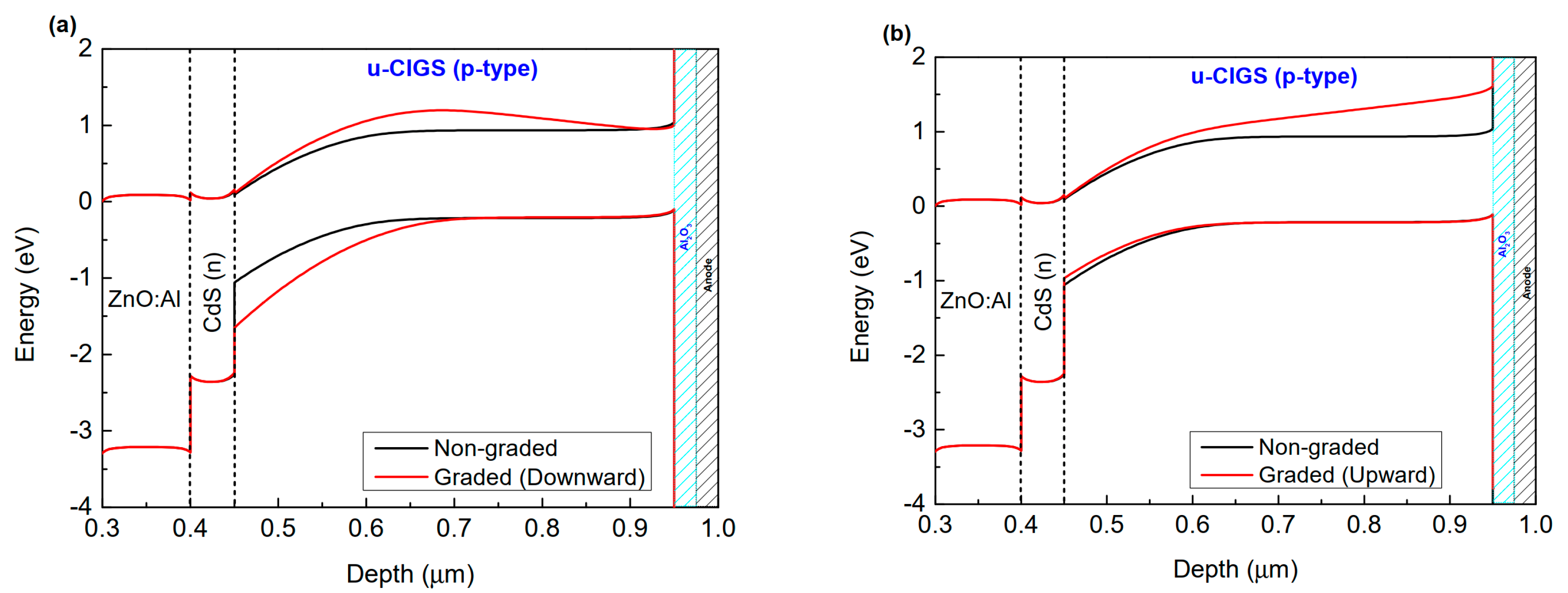
Figure 4.
Electron concentration and recombination rate in u-CIGS solar cell for different absorber bandgap configuration.
Figure 4.
Electron concentration and recombination rate in u-CIGS solar cell for different absorber bandgap configuration.
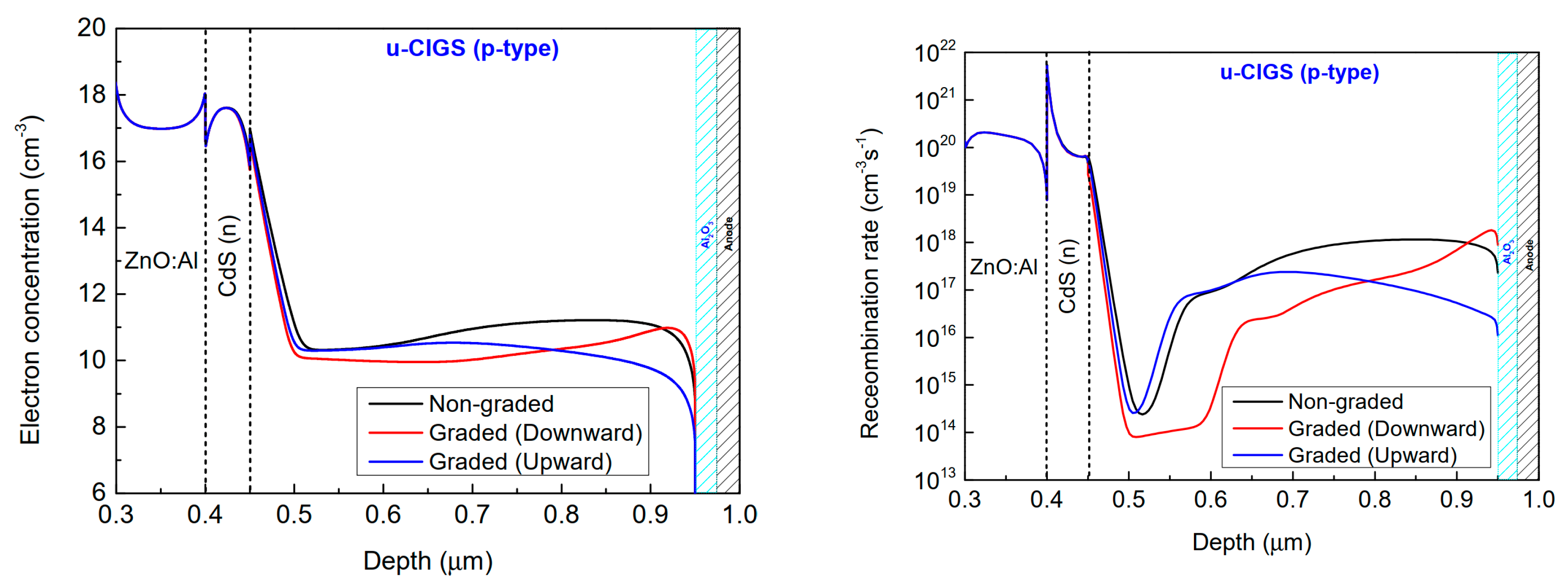
Figure 5.
Ban diagram for non-graded bandgap and graded, increasing toward front and back surfaces (red) and J–V curves of the investigated u-CIGS solar cell models.
Figure 5.
Ban diagram for non-graded bandgap and graded, increasing toward front and back surfaces (red) and J–V curves of the investigated u-CIGS solar cell models.

Figure 6.
PV characteristics of u-CIGS cells for different electron affinities of the absorber.
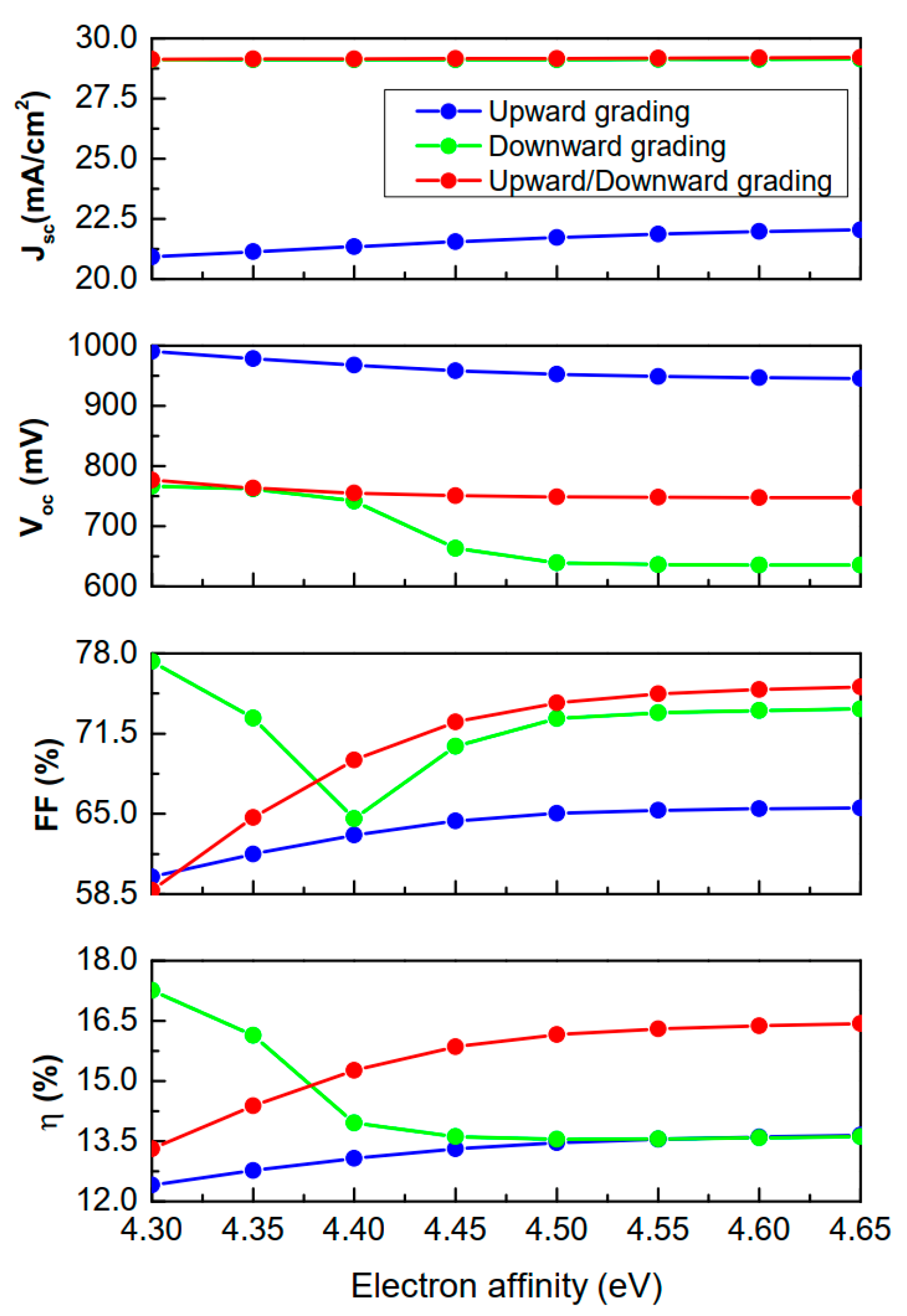
Figure 7.
PV characteristics of u-CIGS cells for different absorber doping densities.

Figure 8.
Variation of ultrathin CIGS solar cell parameters with operating temperature.
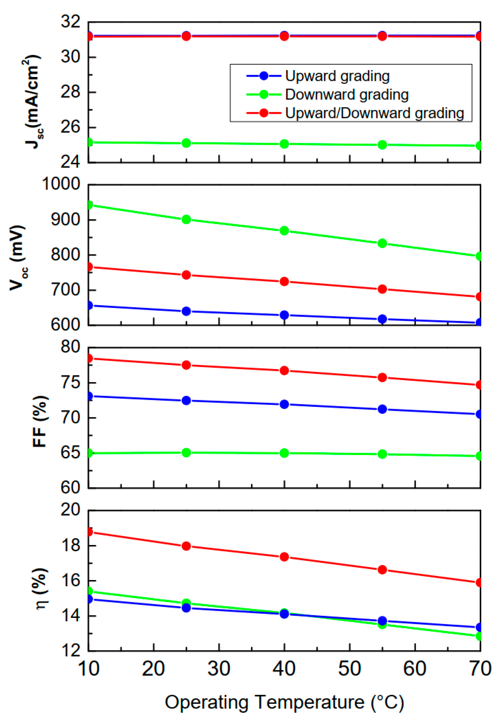
Figure 9.
PV characteristics of u-CIGS cells for different ZnS doping densities and electron affinities.
Figure 9.
PV characteristics of u-CIGS cells for different ZnS doping densities and electron affinities.
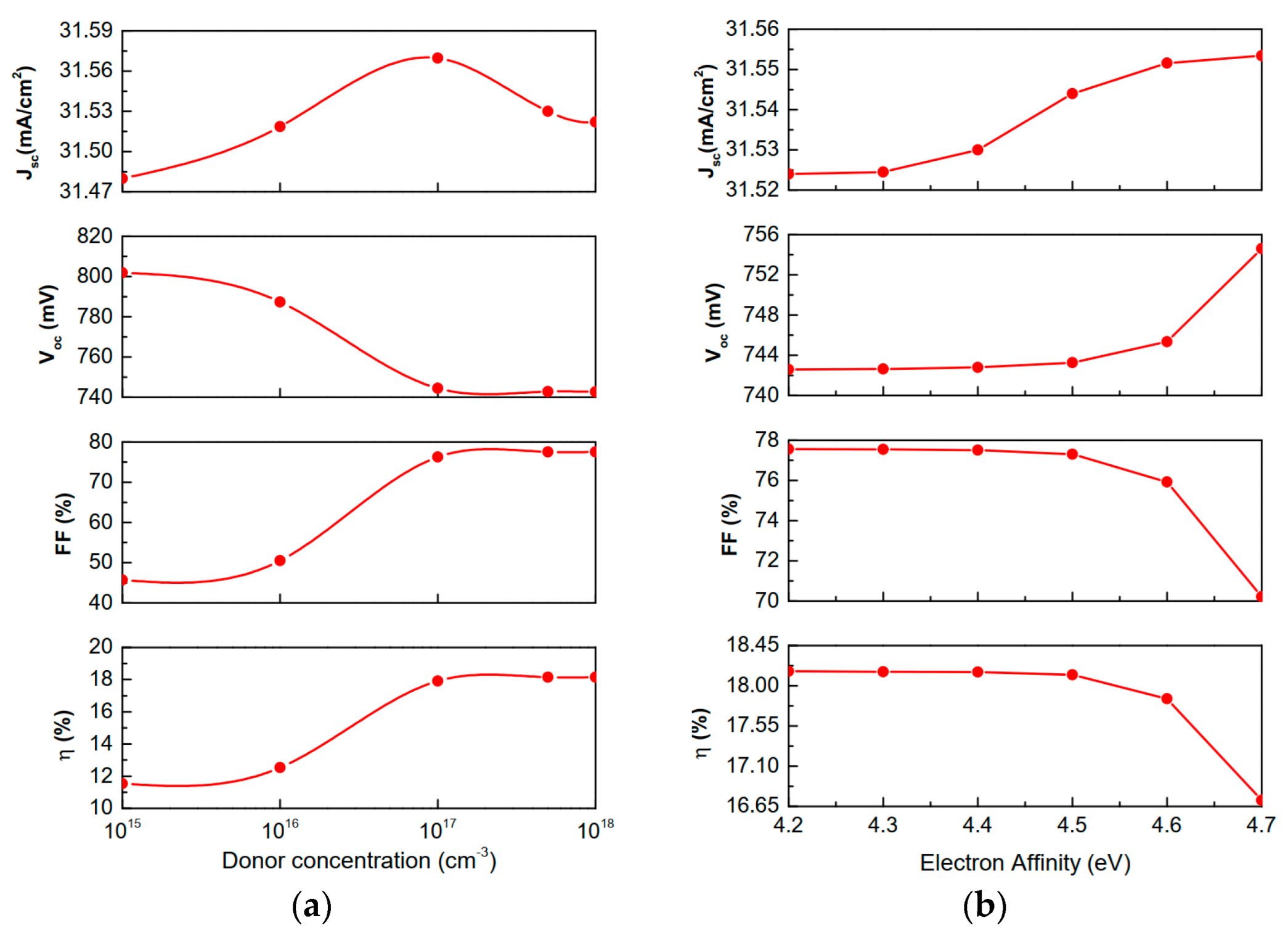
Figure 10.
Simulated J–V curves of different u-CIGS solar cell models and quantum efficiency characteristics curves of optimized doubled-graded u-CIGS solar cell model using a 50 nm-thick for both ZnS (Red) and CdS (Green) layers.
Figure 10.
Simulated J–V curves of different u-CIGS solar cell models and quantum efficiency characteristics curves of optimized doubled-graded u-CIGS solar cell model using a 50 nm-thick for both ZnS (Red) and CdS (Green) layers.


Table 1.
Device parameters for a passivated u-CIGS solar cell model [1].
Table 1.
Device parameters for a passivated u-CIGS solar cell model [1].
| Device Characteristics | Symbol | Al:ZnO | ZnO | CdS | ZnS [33] | CIGS |
|---|---|---|---|---|---|---|
| Thickness (nm) | d | 300 | 100 | 50 | 50 | 500 |
| Bandgap (eV) | Eg | 3.3 | 3.3 | 2.4 | 3.6 | 1.15 |
| Affinity (eV) | χe | 4.55 | 4.55 | 4.45 | 4.4 | 4.5 |
| Permitivity | εr | 9 | 9 | 10 | 8.32 | 13.6 |
| CB density of state (cm−3) | Nc | 3.1 × 10¹⁸ | 3.1 × 10¹⁸ | 1.3 × 10¹⁸ | 2.2 × 10¹⁸ | 3.1 × 10¹⁸ |
| VB density of state (cm−3) | Nv | 1.8 × 10¹⁹ | 1.8 × 10¹⁹ | 9.1 × 10¹⁸ | 1.8 × 10¹⁹ | 1.8 × 10¹⁹ |
| Electron thermal velocity (cm/s) | Vtn | 2.4 × 10⁷ | 2.4 × 10⁷ | 3.1 × 10⁷ | 3.1 × 10⁷ | 3.9 × 10⁷ |
| Hole thermal velocity (cm/s) | Vtp | 1.3 × 10⁷ | 1.3 × 10⁷ | 1.6 × 10⁷ | 1.6 × 10⁷ | 1.4 × 10⁷ |
| Mobility of electrons (cm2/V.s) | μn | 100 | 100 | 72 | 250 | 100 |
| Mobility of holes (cm2/V.s) | μp | 31 | 31 | 20 | 40 | 12.5 |
| Donor concentration, ND (cm−3) | Nd | 5 × 10¹⁸ | 1 × 10¹⁷ | 5 × 10¹⁷ | 5 × 10¹⁷ | - |
| Acceptor concentration, NA (cm−3) | Na | - | - | - | - | 3 × 10¹⁶ |
| Defect density (cm3) | Nt | 1 × 10¹⁶ | 1 × 10¹⁶ | 1 × 10¹⁶ | 1 × 10¹⁶ | 1 × 10¹⁴ |
Table 2.
Investigated model characteristics.
| Cell Parameters | This Work | Ref. [1] | Ref. [2] |
|---|---|---|---|
| Jsc (mA/cm2) | 26.93 | 26.79 | 26.70 |
| Voc (mV) | 629.175 | 661.58 | 621.27 |
| FF (%) | 72.92 | 71.54 | 74.85 |
| Pmax (W/m2) | 247.148 | - | - |
| η (%) | 12.35 | 12.68 | 12.41 |
Table 3.
Characteristics for the investigated u-CIGS models.
| Device Characteristics | Standard (1.15 eV) | Graded Bandgap (Downward) | Graded Bandgap (Upward) | Double-Graded Bandgap (Downward/Upward) |
|---|---|---|---|---|
| J0 (mA/cm2) | 3.17 × 10⁻⁷ | 3.25 × 10⁻⁷ | 3.23 × 10⁻⁷ | 3.18 × 10⁻⁷ |
| Jsc (mA/cm2) | 26.93 | 21.72 | 29.12 | 29.16 |
| Voc (mV) | 629.175 | 952.252 | 639.544 | 748.778 |
| FF (%) | 72.92 | 65.04 | 72.71 | 73.98 |
| Pmax (W/m2) | 247.148 | 269.16 | 270.86 | 323.11 |
| η (%) | 12.35 | 13.45 | 13.54 | 16.15 |
Table 4.
Comparison of different investigated u-CIGS solar cell models.
| u-CIGS Devices (25 °C) | Jsc (mA/cm2) | Voc (mv) | FF (%) | η (%) |
|---|---|---|---|---|
| Eg downward graded (ZnS buffer layer) | 25.10 | 901.01 | 65.04 | 14.71 |
| Eg upward graded (ZnS buffer layer) | 31.18 | 639.52 | 72.45 | 14.44 |
| Eg double-graded (CdS buffer layer) | 31.22 | 742.66 | 77.50 | 17.97 |
| Eg double-graded (ZnS buffer layer) | 31.53 | 742.78 | 77.50 | 18.15 |
Disclaimer/Publisher’s Note: The statements, opinions and data contained in all publications are solely those of the individual author(s) and contributor(s) and not of MDPI and/or the editor(s). MDPI and/or the editor(s) disclaim responsibility for any injury to people or property resulting from any ideas, methods, instructions or products referred to in the content. |
© 2023 by the authors. Licensee MDPI, Basel, Switzerland. This article is an open access article distributed under the terms and conditions of the Creative Commons Attribution (CC BY) license (https://creativecommons.org/licenses/by/4.0/).
Share and Cite
MDPI and ACS Style
Boukortt, N.E.I.; Patanè, S.; Hadri, B.; Crupi, G.
Graded Bandgap Ultrathin CIGS Solar Cells
. Electronics 2023, 12, 393.
https://doi.org/10.3390/electronics12020393
AMA Style
Boukortt NEI, Patanè S, Hadri B, Crupi G.
Graded Bandgap Ultrathin CIGS Solar Cells
. Electronics. 2023; 12(2):393.
https://doi.org/10.3390/electronics12020393
Boukortt, Nour El I., Salvatore Patanè, Baghdad Hadri, and Giovanni Crupi.
2023. "Graded Bandgap Ultrathin CIGS Solar Cells
" Electronics 12, no. 2: 393.
https://doi.org/10.3390/electronics12020393
Note that from the first issue of 2016, this journal uses article numbers instead of page numbers. See further details here.