Abstract
This article demonstrates the possibility of creating memory devices based on polycrystalline mayenite. In the course of the study, structural characterization (XRD, TEM) of ceramic samples of mayenite was carried out, as well as a study of the spectral (THz range) and electrophysical characteristics. Materials obtained by calcination at high (1360–1450 °C) temperatures in an inert argon atmosphere differ in the degree of substitution of oxygen anions O2− for electrons, as indicated by the data on the unit cell parameters and dielectric constant coefficients in the range of 0.2–1.3 THz, as well as differences in the conducting properties of the samples under study by more than five orders of magnitude, from the state of the dielectric for C12A7:O2− to the conducting (metal-like) material in the state of the C12A7:e− electride. Measurements of the current–voltage characteristics of ceramic C12A7:e− showed the presence of memristive states previously detected by other authors only in the case of single crystals. The study of the stability of switching between states in terms of resistance showed that the values of currents for states with high and low resistance remain constant up to 180 switching cycles, which is two times higher than the known literature data on the stability of similar prototypes of devices. It is shown that such samples can operate in a switch mode with nonlinear resistance in the range of applied voltages from –1.3 to +1.3 V.
1. Introduction
The interest in materials based on calcium aluminates with a mayenite structure (12CaO·7Al2O3, designated as C12A7) is largely due to the possibility of varying their functional properties over a wide range due to changes in the composition of the anionic sublattice, which occur with the retention of the cationic framework of the mayenite structure [1,2,3,4,5,6]. The positive charge of the 4+ cationic framework of [Ca24Al28O64]4+ is compensated by the total negative charge of the 4− anions included in the anion sublattice. The chemical and electrophysical properties of such materials can be varied over a very wide range by replacing the X− anions. The unit cell composition of such a compound can be described by the Formula (1):
1 unit cell = [Ca24Al28O64]4+ × 4X−, where X− = H−, O−, O2−, O2−, OH−, Cl−, F−, e−
The most interesting and unusual materials obtained based on mayenite are electrides (X = e−) in which the role of anions is played by electrons. This class of materials was first discovered in the works of the H. Hosono laboratory about 20 years ago [1,2] and it was precisely these works that stimulated the development of work on the study of the properties of inorganic electrodes and the search for possible areas of their use. The greatest development in the practical use of these materials to date has received the direction of work associated with their use as electron-donor carriers for heterogeneous catalysts [7,8,9]. Along with this, several publications have demonstrated the possibility of using this class of inorganic electrodes as a material for creating components of electronic devices. The following are the main properties of C12A7 material in terms of its possible use as a material for the creation of components of electronic devices:
- The low work function (2.1–2.4 eV) makes it possible in principle to use the C12A7:e− electrode for creating economical and efficient cathodes in a variety of devices. Including those using the thermal emission properties of the material [10,11,12]. Recently, the possible use of this material in field-effect transistors, light-emitting diodes, and also as emission elements in displays [13,14] has been discussed. In the reviews [15,16], the possible areas of using this material for the creation of components of electronic devices are presented in sufficient detail.
- Another possibility of using the C12A7 material is the creation of memristive memory elements based on it. The principle of operation of such elements is based on the reversible diffusion of oxygen ions in the C12A7:e−/C12A7:O2−—a system under the action of an electric field. The fundamental possibility of creating such elements was demonstrated in [17] and is also reflected in the review [16]. It should be noted that a single-crystal material was used in this work as a material for creating such elements. At the same time, of considerable interest is the practical use of polycrystalline materials, the technology of obtaining and controlling the conductivity (from the state of the dielectric to metallic) which can be much simpler and cheaper.
This work aimed to obtain information on the electrophysical and spectral characteristics of several polycrystalline samples of mayenite with various degrees of substitution of oxygen anions by electrons and to assess the possibility of the formation of memristive states in such systems.
2. Materials and Methods
2.1. Fabrication Technique and Fabrication Setup
In this work, the method of synthesis of mayenite previously described in [18,19,20] was used. Aluminum hydroxide (Condea Pural SB—1, pseudo-boehmite, >99.9%) and calcium carbonate (Reachim, >99.97%) were used as starting materials for the synthesis. The first stage of the synthesis was to obtain CaO by decomposing CaCO3 in a muffle furnace in the air at 950 °C for 6 h. After that, the resulting CaO was added to a suspension of aluminum hydroxide in distilled water at room temperature with continuous stirring. The final ratio of the components corresponds to the stoichiometry of mayenite (12CaO·7Al2O3). The mixture was thoroughly stirred in distilled water for 10 h, filtered, and dried at 110 °C. Then, it was calcined in a muffle furnace in air at 500 °C for 6 h. The samples obtained were successively calcined in an Ar flow at high temperatures (>1300 °C). The initial sample C12A7-500 was heated at a rate of 3 °C/min, followed by holding at the specified temperature for 6 h. For characterization and investigation of electro-physical properties, a sample was taken at four temperature points: at 1360 °C, 1380 °C, 1390 °C, and 1450 °C. The appearance of the selected samples is shown in Figure 1, which in the future will be designated, respectively, as C12A7-1360 (white sample), C12A7-1380 (green), C12A7-1390 (dark green), and C12A7-1450 (black, electride).
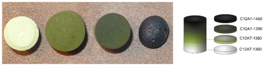
Figure 1.
Photography and cutting scheme of samples C12A7-1360, C12A7-1380, C12A7-1390, and C12A7-1450 (from left to right).
2.2. Characterization Methods
X-ray powder diffraction studies were performed on an ARL X’tra diffractometer (ThermoFisher Scientific, Switzerland, Basel) with a radiation source Cu–Ka (λ = 1.5418 Å). The recording of diffraction patterns was carried out in the range of 2θ = 15–85°. The figures show inserts in the range up to 60°. The step was 0.05°, the signal accumulation time was 3 s at each point. The processing of diffraction patterns and semiquantitative phase analysis was carried out by refining the full profile by the Rietveld method in the GSAS-II program [21].
HRTEM images were obtained on a JEM-2200FS transmission electron microscope (JEOL, Japan) with a spherical aberration corrector at an accelerating voltage of 200 kV. Initially, a sample in the form of a finely dispersed powder was deposited on the grid using an ultrasonic disperser.
To measure absorption spectra in the THz range, disks about 1 mm thick were cut out of the samples. The measurements were carried out using a small-sized broadband pulsed terahertz time–domain spectrometer (THz–TDS) located at the Institute of Automation and Electrometry SB RAS, the spectral range of which is 0.1–2.7 THz, with a peak in the spectral dynamic range of >70 dB at a frequency of 0.3 THz. A detailed description of the setup is given in [22,23]. The schematic of the THz–TDS is shown in Figure 2.
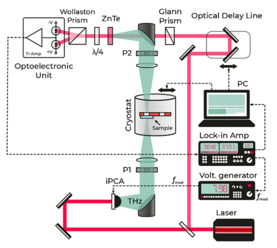
Figure 2.
Schematic diagram of the THz–TDS.
The scanning range of the THz–TDS is 60 ps, which corresponds to a spectral resolution of 20 GHz. The scanning step was 125 fs. The averaging time at each point was 0.21 s with the time constant of the lock-in amplifier filter equal to 30 ms. In the study, a liquid nitrogen cryostat with fused silica windows and a resistive heater was used. The sample holder had two diaphragms with a diameter of 7 mm in the lower flat part (Figure 2). The sample under study was fixed on one of the diaphragms, the other was used to record reference THz signals. After processing terahertz signals in the same way as described in [24], the values of the real and imaginary parts of the permittivity were obtained.
Porosity of the polycrystalline samples can be the main factor that influences permittivity so we made additional recalculations. The density values were measured by the helium pycnometry method on the automatic ULTRAPYC-1200e device (Quantachrome Instruments, Boynton Beach, FL, USA) with ±0.03% accuracy. Obtained values were used for the estimation of sample porosity.
Influence of porosity was taken into account using the Maxwell–Garnett effective medium model with spherical inclusions [25]:
where —is the initially measured complex dielectric constant of the samples, —dielectric constant of inclusion (air), —the required dielectric constant of the medium (medium) i.e., mayenite, is the factor of filling the medium with particles (the ratio of the total volume of voids to the entire volume of the medium).
The calculations were carried out in such a way that Re[] of the mayenite sample coincided with the value of ε1 for the single-crystal mayenite samples presented in [26,27] since the material density makes the main contribution to the real part of the dielectric susceptibility.
The study of the electrophysical characteristics of the obtained samples was carried out on metal–mayenite–metal structures. The upper nickel electrodes with a thickness of 200 nm and an area of 0.5 mm2 were deposited through a mask by magnetron sputtering in an Ar atmosphere. On the reverse side, a continuous nickel layer of the same thickness was deposited. The I–V characteristics (current–voltage characteristics) of the structures obtained and the stability of the operation of the C12A7-1450 sample were measured at room temperature in DC mode using a B2902A two-channel source-meter (Agilent, Santa Clara, CA, USA) with micropositioners with probes connected to it.
The voltage sweep was performed from 0 to 50 V for samples C12A7-1360, C12A7-1380, and C12A7-1390, and from –2 to 2 V for C12A7-1450. The measurements were carried out stepwise at the end of each step. The measurement duration at each point was 0.2 s for C12A7-1360, C12A7-1380, and C12A7-1390, and 0.5 s for C12A7-1450. The measurement parameters were set and the data were read out using the Agilent B2900A Quick I/V Measurement Software.
3. Results and Discussion
3.1. XRD Analysis
The samples were analyzed by XRD to confirm their phase composition and structure of the obtained material. According to XRD data (Figure 3, Table 1), the mayenite sample C12A7-1360 predominantly contains the Ca12Al14O33 phase (C12A7, JCPDS No 9-413), with small impurities of Ca3Al2O6 (C3A, JCPDS No 38-1429) and CaAl2O4 (CA, JCPDS No 23-1036). In the sample C12A7-1380, in that the formation of the electride state C12A7:e− began, in addition to the main phase, a large amount (from 20 to 40%) of impurity phases C3A and CA were detected. It should be noted that both C12A7-1380 and C12A7-1390 samples demonstrated similar diffractograms. At the same time, C12A7-1450 is a single-phase material (up to 95%) with an insignificant admixture of CA.
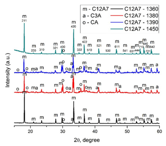
Figure 3.
XRD patterns of the C12A7-samples upon calcination from 1360 to 1450 °C.

Table 1.
XRD parameters for C12A7 samples.
The lattice parameter of the mayenite phase (Table 1) slightly increases during these transformations from 11.998 to 12.004 Å. A gradual increase in the calcination temperature leads to the decomposition of the mayenite phase into phases C3A and CA, the content of which in the system is rather high. In the literature [28,29], it was indicated earlier that the process of oxygen release from the structure can be accompanied by rearrangements of the latter, with its stratification into aluminates of a different composition. Then, with a gradual increase in temperature in an inert atmosphere, an oxygen-deficient electride state C12A7:e− is formed. The increased value of the lattice parameter indicates the presence of oxygen vacancies at the crystallographic O3 positions, and, as a consequence, the presence of electrons in the unit cells of mayenite [30,31].
3.2. TEM Analysis
The HRTEM micrographs show the microstructure of the initial C12A7-1360 (Figure 4a,b) and final C12A7-1450 (Figure 4c,d) samples. The morphology of samples was presented by flat well-crystallized particles of large size (0.5–5 µm). It is clearly shown that samples have the analogous microstructure and no significant differences in it. To estimate the interplanar distances of the phase, a Fourier transform of the obtained images of the crystal structure was carried out. The obtained values, in particular 0.4898 nm, are in good agreement with the XRD data (0.4897 nm for the 211 reflection). This also confirms the presence of a mayenite-type structure.
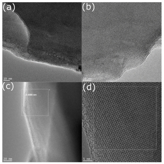
Figure 4.
Microstructure of the mayenite particles in samples C12A7-1360 (a,b) and C12A7-1450 (c,d).
3.3. Terahertz Spectroscopy
The value of the measured density is approximately 2.65 g/cm3. Thus, we specified that η = 0.13 (Equation (2)), which corresponds to a density of 87% for our initially synthesized samples. The resulting values of the real ε1 and imaginary ε2 parts of the dielectric constant of our materials are shown in Figure 5. For comparison, we also adapted the data from the article [26] (C12A7-P, C12A7-H), with which there is a good agreement.
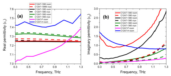
Figure 5.
Spectra of the real (a) and imaginary (b) parts of the dielectric constant of mayenite, measured at temperatures of 24 °C (room) and −192 °C (cryo).
An analysis of the spectra shows that ongoing from pure mayenite to the electric phase, an increase in ε2 to low frequencies is observed. This is in good agreement with the data obtained by Hosono et al. (see the curve for C12A7-H in Figure 5) and indicates an increase in the concentration of free charge carriers, which is expressed in an increase in the plasma frequency and a gradual increase in attenuation for the low-frequency part of the spectrum. We also note that this is also the reason why we were unable to study the C12A7-1450 electride sample. Since the concentration of free charge carriers in it is so high that the plasma frequency already lies above the spectral range of our THz–TDS, this leads to total reflection of the THz wave from the sample and does not allow obtaining a signal in transmission geometry. From the ε2 graphs in Figure 5, we can conclude that the concentration of charge carriers in the C12A7-1390 sample corresponds to the values for C12A7-H from [26] and has a value of ~1018 cm−3. At the same time for C12A7-1380, this value is noticeably lower. A sharper increase in ε2 in our case is most likely associated with the scattering of high-frequency THz radiation by air pores in the samples.
Cooling of our samples did not significantly affect ε1. However, a noticeable change was observed in ε2, in particular, a decrease in the low-frequency region. Presumably, this is due to the capture of free charge carriers during cooling of the material.
3.4. Electrophysical Characterization (I–V Curves)
The I–V characteristics of all samples are shown in Figure 6. Three samples have shown hysteresis, which is characteristic of dielectrics. The currents for samples C12A7-1360, C12A7-1380, and C12A7-1390 are 3.2 × 10 −11 A, 2.5 × 10 −8 A, and 6.2 × 10 −9 A, respectively, at a voltage of 200 V. High voltages were not applied to the sample C12A7-1450 to preserve the integrity of the sample, although, an almost vertical I–V curve was observed. This indicates an exceedingly lower resistance of C12A7-1450 compared with other samples.
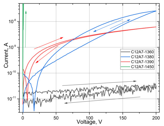
Figure 6.
I–V characteristics of samples C12A7-1360, C12A7-1380, C12A7-1390, and C12A7-1450. The arrows indicate the direction of the recording.
The difference in current between samples C12A7-1360, C12A7-1380, and C12A7-1390 can be explained by the fact that at a temperature of 1380 °C oxygen ions O2− are replaced by electrons e−, and an electride phase is formed. In connection with this, the concentration of free charge carriers (presumably electrons) increases. This suggestion is also confirmed by the spectra analysis of the imaginary part of the dielectric constant ε2.
The I–V characteristic of the C12A7-1380 sample increases exponentially, which indicates the diode properties of the sample. In addition, the higher current during scanning in the opposite direction is explained by the low response rate of the internal electric field of the C12A7-1380 sample. Most likely, this behavior is associated with the uneven formation of the electric mayenite phase over the thickness during heat treatment.
The first I–V characteristics of the C12A7-1450 sample were studied in the range of –2 to 2 V with a voltage step of 0.01 V and the current limitation of 10−6 A (Figure 7). The arrows show the direction of the data scanning. The measurements started at 0 V and continued in the direction of negative voltages. It can be seen from the I–V characteristic that hysteresis exists at negative polarity. When the voltage reaches −1.4 V, a sharp current increase occurs, and the source switches to the current mode due to the limitation of the current value (in our case, 10−6 A). During the reverse stroke, the structure is at this current limitation down to −1 V and then the sample exhibits a lower resistance. That is, at −1.4 V, there was a transition from a high-resistance (HR) state to a low-resistance (LR) state. The window between states in this region is two orders of magnitude in current. Then, a positive bias from 0 to 1.6 V was applied to the structure. With increasing voltage, the current increases and reaches the specified limit. Furthermore, with decreasing voltage, the current also decreases already in a state with lower resistance. In the region of positive voltages, the I–V characteristics are unstable, which indicates unipolar switching between the states, i.e., switching occurs only in one polarity. Similar I–V characteristics are observed in memristor structures [32,33]. Moreover, in the second half of the cycle, there is a zero-current bias in the HR state. This feature indicates the accumulation of charges in the bulk of the structure [27]. The switching effects from high-resistance to low-resistance states and back, typical of memristors, were not observed for the samples C12A7-1360, C12A7-1380, and C12A7-1390. Therefore, the memristor properties of sample C12A7-1450 are described in detail below.
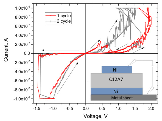
Figure 7.
I–V characteristic of the C12A7-1450 sample. The arrows indicate the direction of the recording.
Figure 8 shows the I–V characteristics for the C12A7-1450 sample with three sweep cycles. The variable parameter in this group of measurements was the initial scanning voltage of 0.6 V, 1 V, and 1.6 V. At an initial point of 0.6 V, the switching voltage was –0.68 V, while at 1 V, the switching voltage was −0.92 V, and when the initial point was increased to 1.6 V, the switching voltage became −1.16 V (in Figure 8, the switching points are denoted as A, B, and C, respectively). Arrows indicate the direction of data measurement. Thus, Figure 8 illustrates the dependence of the switching voltage on the starting point. The switching voltage between the states (in terms of resistance) increases with an increase in the initial voltage.
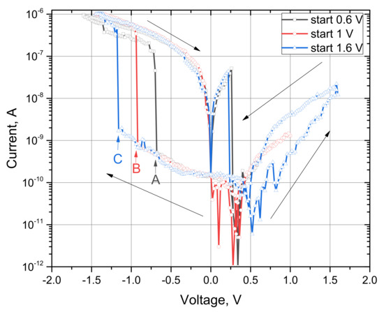
Figure 8.
I–V characteristics of the C12A7-1450 sample at different initial voltages.
A study of the LR-state on-state current stability is represented in Figure 9. The measurements were carried out stepwise according to the scheme shown in Figure 9b. The current limit was 10−6 A. In the first few seconds (Figure 9a), there is a switch between off and on states. This sets the current corresponding to this voltage. Then, after 50 s, the voltage decreases in steps to −1.05 V and it is maintained at this value for the next 50 s. The current corresponding to this voltage also decreases and remains stable until the next voltage change of −0.5V. The current in the sections with a voltage of −1.05 V and −0.5 V is stable and corresponds to the current in the I–V characteristic in Figure 7 and Figure 8. Furthermore, the voltage also rises in steps to the initial value of −1.6V. As the voltage changes, the current also increases. Thus, this sample can operate in the mode of a switch with a nonlinear resistance.
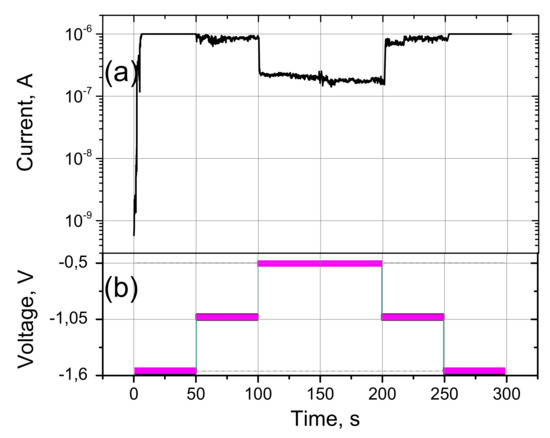
Figure 9.
Investigation of current stability: (a) current versus time for the sample C12A7-1450 and (b) measurement scheme.
Furthermore, on-state storage studies were conducted in order to verify the memristor characteristic of C12A7-1450. Initially, the sample was switched to an LR state. After switching to a different state, the contacts on the sample were disconnected from the power supply for a few minutes (<10 min). Furthermore, the current dependence on time was measured (Figure 10) at a constant voltage of –0.5 V. When disconnected from the network current it was about 5 × 10 −8 A, which is much less than it should be on the I–V characteristic in Figure 9. The current decreased from 10−7 to 10−8 in a few minutes without a power supply. A decrease in the current indicates a very short storage time for the LR state and volatility, i.e., energy dependence, of the C12A7-1450 sample.
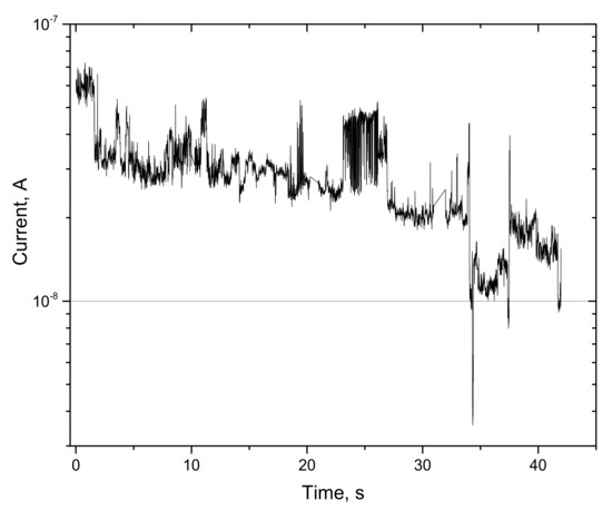
Figure 10.
Dependence of current on time after disconnection from the network for the sample C12A7-1450.
Figure 11 shows a study of the stability of switching between the states in terms of resistance. One switching cycle begins with a voltage pulse corresponding to the switch–off voltage. After that, at a given readout voltage, the current was measured, which corresponds to the off stage. Then, a voltage pulse was applied corresponding to the turn-on voltage. After that, at a given readout voltage, the current was measured, which corresponds to the turn-on stage. Furthermore, the switching cycles are repeated N times. The duration of the switching pulses was 100 ms, with a period of 500 ms. The amplitude of the two corresponding pulses was 1 and –1.6 V, respectively. The reading voltage was –0.5 V. In Figure 11, it is noticeable that the switching between states was relatively stable. However, one can notice several cycles that have not switched to a LR state. The resistances were in the order of 109 Ω in the off state and 5 × 10 6 Ω in the on state. In the other work on the study of bistable resistive switching of C12A7, cyclic switching was also investigated [17]. By comparing the data, it can be seen that the number of withstood cycles is higher [17]. Comparable dependencies were reported for other memristor materials [32].
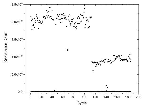
Figure 11.
Cyclic switching between states by resistance for the sample C12A7-1450.
4. Conclusions
The possibility of creating a memory element based on polycrystalline mayenite synthesized from hydroxide precursors has been demonstrated. Materials after heat treatment at high (1360–1450 °C) temperatures in an inert argon atmosphere differ in the degree of substitution of electrons with oxygen anions O2− as evidenced by the data on the unit cell parameters and dielectric constant in the range 0.2–1.3 THz. There is a noticeable difference in the conductive properties of the samples in this study. Measurements of the I–V characteristics of the polycrystalline C12A7:e− ceramics showed the presence of memristive states, previously discovered by other researchers only in single-crystal materials. The study of the stability of switching between the conductive states in terms of resistance showed that the values of current for states with high and low resistance remain constant up to 180 switching cycles, which is two times higher than the known literature data on the stability of similar prototypes of memory devices. Such samples can operate in a switching mode with a nonlinear resistance in the range of applied voltages from –1.3 to +1.3 V. It paves a way for the production of switch elements based on polycrystalline C12A7 materials. Such elements are analogous memristors that can be used as an elemental base for creation of analog neural networks.
Author Contributions
Conceptualization, N.A.N. and A.M.V.; data curation, I.D.Y.; funding acquisition, P.V.G.; investigation, A.A.R., I.D.Y., N.A.N., A.V.K., G.N.K. and G.K.K.; methodology, A.V.K., G.N.K. and A.M.V.; project administration, P.V.G.; resources, A.M.V.; visualization, A.A.R.; writing—original draft, A.A.R., I.D.Y., A.V.K. and P.V.G.; writing—review and editing, A.A.R. All authors have read and agreed to the published version of the manuscript.
Funding
This research was funded by the Ministry of Education and Science of the Russian Federation, grant No. FSUS-2020-0029, in terms of sample preparation and analysis.
Acknowledgments
The authors acknowledge the NSU Shared Equipment Centers “Applied Physics” and “VTAN”. The authors acknowledge the Shared Equipment Center “Spectroscopy and Optics” of the Institute of Automation and Electrometry SB RAS for the provided terahertz time-domain spectrometer. The authors acknowledge M. I. Mironova for help with electron microscopy, V. A. Volodin for help with Raman spectroscopy, A. O. Geydt for help with translation, and An. A. Rybak for help with drawings.
Conflicts of Interest
The authors declare no conflict of interest. The funders had no role in the design of the study; in the collection, analyses, or interpretation of data; in the writing of the manuscript, or in the decision to publish the results.
References
- Hayashi, K.; Matsuishi, S.; Kamiya, T.; Hirano, M.; Hosono, H. Light-induced conversion of an insulating refractory oxide into a persistent electronic conductor. Nature 2002, 419, 462–465. [Google Scholar] [CrossRef] [PubMed]
- Hayashi, K.; Hirano, M.; Matsuishi, S.; Hosono, H. Microporous crystal 12CaO·7Al2O3 encaging abundant O-radicals. J. Am. Chem. Soc. 2002, 124, 738–739. [Google Scholar] [CrossRef]
- Matsuishi, S.; Toda, Y.; Miyakawa, M.; Hayashi, K.; Kamiya, T.; Hirano, M.; Tanaka, I.; Hosono, H. High-density electron anions in a nanoporous single crystal: [Ca24Al28O64]4+(4e-). Science 2003, 301, 626–629. [Google Scholar] [CrossRef]
- Kim, S.W.; Hosono, H. Synthesis and properties of 12CaO·7Al2O3 electride: Review of single crystal and thin film growth. Philos. Mag. 2012, 92, 2596–2628. [Google Scholar] [CrossRef]
- Galuskin, E.; Galuskina, I.; Vapnik, Y.; Murashko, M. Molecular Hydrogen in Natural Mayenite. Minerals 2020, 10, 560. [Google Scholar] [CrossRef]
- Hosono, H.; Kitano, M. Advances in Materials and Applications of Inorganic Electrides. Chem. Rev. 2021, 121, 3121–3185. [Google Scholar] [CrossRef]
- Kitano, M.; Inoue, Y.; Yamazaki, Y.; Hayashi, F.; Kanbara, S.; Matsuishi, S.; Yokoyama, T.; Kim, S.W.; Hara, M.; Hosono, H. Ammonia synthesis using a stable electride as an electron donor and reversible hydrogen store. Nat. Chem. 2012, 4, 934–940. [Google Scholar] [CrossRef] [PubMed]
- Hara, M.; Kitano, M.; Hosono, H. Ru-Loaded C12A7:e(-) Electride as a Catalyst for Ammonia Synthesis. ASC Catal. 2017, 7, 2313–2324. [Google Scholar] [CrossRef]
- Kammert, J.; Moon, J.; Cheng, Y.Q.; Daemen, L.; Irle, S.; Fung, V.; Liu, J.; Page, K.; Ma, X.H.; Phaneuf, V.; et al. Nature of Reactive Hydrogen for Ammonia Synthesis over a Ru/C12A7 Electride Catalyst. J. Am. Chem. Soc. 2020, 142, 7655–7667. [Google Scholar] [CrossRef]
- Toda, Y.; Kim, S.W.; Hayashi, K.; Hirano, M.; Kamiya, T.; Hosono, H.; Haraguchi, T.; Yasuda, H. Intense thermal field electron emission from room-temperature stable electride. Appl. Phys. Lett. 2005, 87, 254103. [Google Scholar] [CrossRef]
- Yoshizumi, T.; Hayashi, K. Thermionic Electron Emission from a Mayenite Electride-Metallic Titanium Composite Cathode. Appl. Phys. Express 2013, 6, 015802. [Google Scholar] [CrossRef]
- Rand, L.P.; Williams, J.D. A Calcium Aluminate Electride Hollow Cathode. IEEE Trans. Plasma Sci. 2015, 43, 190–194. [Google Scholar] [CrossRef] [Green Version]
- Yanagi, H.; Kim, K.B.; Koizumi, I.; Kikuchi, M.; Hiramatsu, H.; Miyakawa, M.; Kamiya, T.; Hirano, M.; Hosono, H. Low Threshold Voltage and Carrier Injection Properties of Inverted Organic Light-Emitting Diodes with [Ca24Al28O64] 4+(4e-) Cathode and Cu2-xSe Anode. J. Phys. Chem. C 2009, 113, 18379–18384. [Google Scholar] [CrossRef]
- Feizi, E.; Ray, A.K. 12CaO·7Al2O3 Ceramic: A Review of the Electronic and Optoelectronic Applications in Display Devices. J. Disp. Technol. 2016, 12, 451–459. [Google Scholar] [CrossRef] [Green Version]
- Zahedi, M.; Ray, A.K.; Barratt, D. Novel Binary Calcia-Alumina Systems for device Applications. Sci. Adv. Mater. 2009, 1, 107–120. [Google Scholar] [CrossRef]
- Hosono, H.; Hayashi, K.; Kamiya, T.; Atou, T.; Susaki, T. New functionalities in abundant element oxides: Ubiquitous element strategy. Sci. Technol. Adv. Mater. 2011, 12, 034303. [Google Scholar] [CrossRef] [Green Version]
- Adachi, Y.; Kim, S.W.; Kamiya, T.; Hosono, H. Bistable resistance switching in surface-oxidized C12A7:e− single-crystal. Mater. Sci. Eng. B 2009, 161, 76–79. [Google Scholar] [CrossRef]
- Volodin, A.M.; Zaikovskii, V.I.; Kenzhin, R.M.; Bedilo, A.F.; Mishakov, I.V.; Vedyagin, A.A. Synthesis of Nanocrystalline Calcium Aluminate C12A7 under Carbon Nanoreactor Conditions. Mater. Lett. 2017, 189, 210–212. [Google Scholar] [CrossRef]
- Yakovlev, I.V.; Volodin, A.M.; Papulovskiy, E.S.; Andreev, A.S.; Lapina, O.B. Structure of Carbon-Coated C12A7 Electride via Solid-State NMR and DFT Calculations. J. Phys. Chem. C 2017, 121, 22268–22273. [Google Scholar] [CrossRef]
- Kapishnikov, A.V.; Kenzhin, R.M.; Koskin, A.P.; Volodin, A.M.; Geydt, P.V. Mayenite Synthesis from Hydroxide Precursors: Structure Formation and Active Sites on Its Surface. Materials 2022, 15, 778. [Google Scholar] [CrossRef] [PubMed]
- Toby, B.H.; Von Dreele, R.B. GSAS-II: The genesis of a modern open-source all-purpose crystallography software package. J. Appl. Cryst. 2013, 46, 544–549. [Google Scholar] [CrossRef]
- Mamrashev, A.A.; Nikolaev, N.A.; Antsygin, V.D.; Bekker, T.B.; Kokh, A.E.; Kokh, K.A.; Lanskii, G.V.; Svetlichny, V.A.; Andreev, Y.M. β-BBO: Optical Properties and Phase-Matching for THz Wave Generation. In Proceedings of the 43rd International Conference on Infrared Millimeter and Terahertz Waves (IRMMW-THz 2018), Nagoya, Japan, 9–14 September 2018. Abstract no. 8510284. [Google Scholar]
- Wang, C.-R.; Pan, Q.-K.; Chen, F.; Lanskii, G.; Nikolaev, N.; Mamrashev, A.; Andreev, Y.; Meshalkin, A. Phase-matching in KTP crystal for THz wave generation at room temperature and 81 K. Infrared Phys. Technol. 2019, 97, 1–5. [Google Scholar] [CrossRef]
- Duvillaret, L.; Garet, F.; Coutaz, J.-L. A reliable method for extraction of material parameters in terahertz time-domain spectroscopy. IEEE J. Sel. Top. Quantum Electron. 1996, 2, 739–746. [Google Scholar] [CrossRef] [Green Version]
- Peiponen, K.-E.; Zeitler, J.A.; Kuwata-Gonokami, M. Terahertz Spectroscopy and Imaging; Springer: Berlin, Germany, 2013; pp. 257–259. [Google Scholar]
- Harimochi, H.; Kitagawa, J.; Ishizaka, M.; Kadoya, Y.; Yamanishi, M.; Matsuishi, S.; Hosono, H. Observation of Jonscher law in ac hopping conduction of the electron-doped nanoporous crystal 12CaO·7Al2O3 in a THz frequency range. Phys. Rev. B 2004, 70, 193104. [Google Scholar] [CrossRef] [Green Version]
- Kitagawa, J.; Ishizaka, M.; Harimochi, H.; Kadoya, Y.; Yamanishi, S.; Matsuishi, S.; Hosono, H. THz time-domain spectroscopy of 12CaO·7Al2O3 (C12A7) containing hopping carriers. In Proceedings of the Joint 29th International Conference on Infrared and Millimeter Waves and 12th International Conference on Terahertz Electronics, Karlsruhe, Germany, 27 September–1 October 2004; pp. 403–404. [Google Scholar] [CrossRef]
- Eufinger, J.P.; Schmidt, A.; Lerch, M.; Janek, J. Novel anion conductors–conductivity, thermodynamic stability and hydration of anion-substituted mayenite-type cage compounds C12A7:X (X = O, OH, Cl, F, CN, S, N). Phys. Chem. Chem. Phys. 2015, 17, 6844–6857. [Google Scholar] [CrossRef] [PubMed] [Green Version]
- Tian, Y.; Pan, X.; Yu, H.; Tu, G. Formation mechanism of calcium aluminate compounds based on high-temperature solid-state reaction. J. Alloys Compd. 2016, 670, 96–104. [Google Scholar] [CrossRef]
- Matsuishi, S.; Nomura, T.; Hirano, M.; Kodama, K.; Shamoto, S.I.; Hosono, H. Direct synthesis of powdery inorganic electride [Ca24Al28O64]4+(e−)4 and determination of oxygen stoichiometry. Chem. Mater. 2009, 21, 2589–2591. [Google Scholar] [CrossRef]
- Salasin, J.R.; Schwerzler, S.E.A.; Mukherjee, R.; Keffer, D.J.; Sickafus, K.E.; Rawn, C.J. Direct Formation and Structural Characterization of Electride C12A7. Materials 2019, 12, 84. [Google Scholar] [CrossRef] [PubMed] [Green Version]
- Volodin, V.A.; Geydt, P.; Kamaev, G.N.; Gismatulin, A.A.; Krivyakin, G.K.; Prosvirin, I.P.; Azarov, I.A.; Fan, Z.; Vergnat, M. Resistive switching in non-stoichiometric germanosilicate glass films containing ge nanoclusters. Electronics 2020, 9, 2103. [Google Scholar] [CrossRef]
- Strukov, D.B.; Snider, G.S.; Stewart, D.R.; Williams, R.S. The missing memristor found. Nature 2008, 453, 80–83. [Google Scholar] [CrossRef] [PubMed]
Publisher’s Note: MDPI stays neutral with regard to jurisdictional claims in published maps and institutional affiliations. |
© 2022 by the authors. Licensee MDPI, Basel, Switzerland. This article is an open access article distributed under the terms and conditions of the Creative Commons Attribution (CC BY) license (https://creativecommons.org/licenses/by/4.0/).