
A High-Gain Multiphase Interleaved Differential Capacitor Clamped Boost Converter

 ,
,  ,
,  and
and 
Abstract
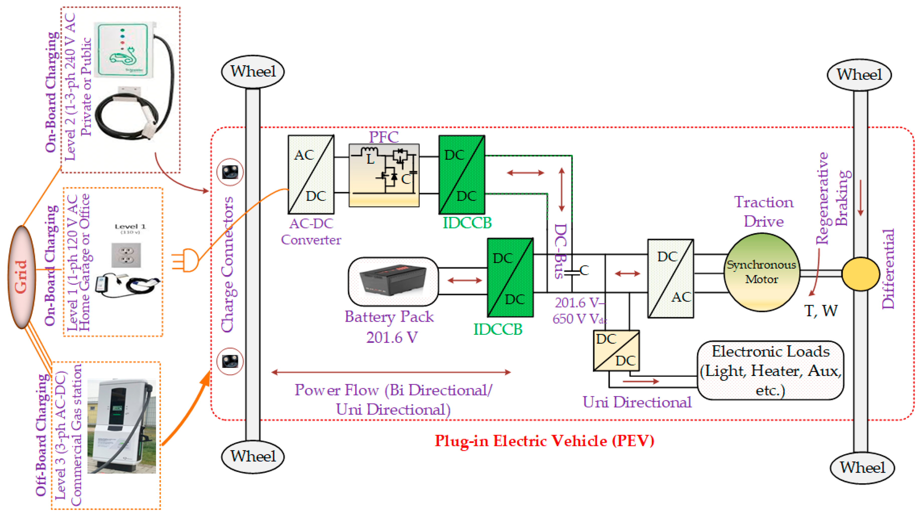
:1. Introduction
2. Modelling of the Two-Phase Converter
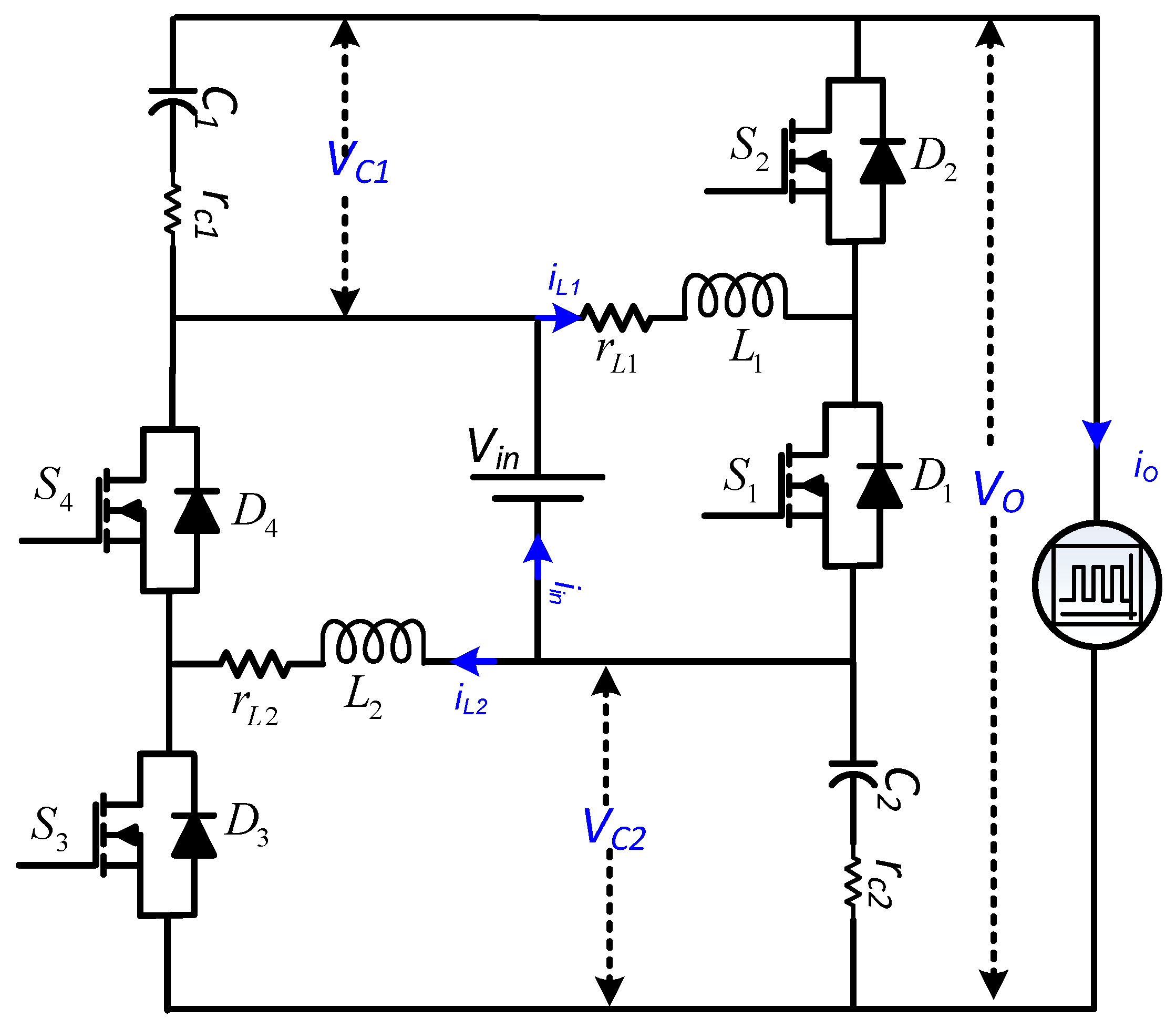
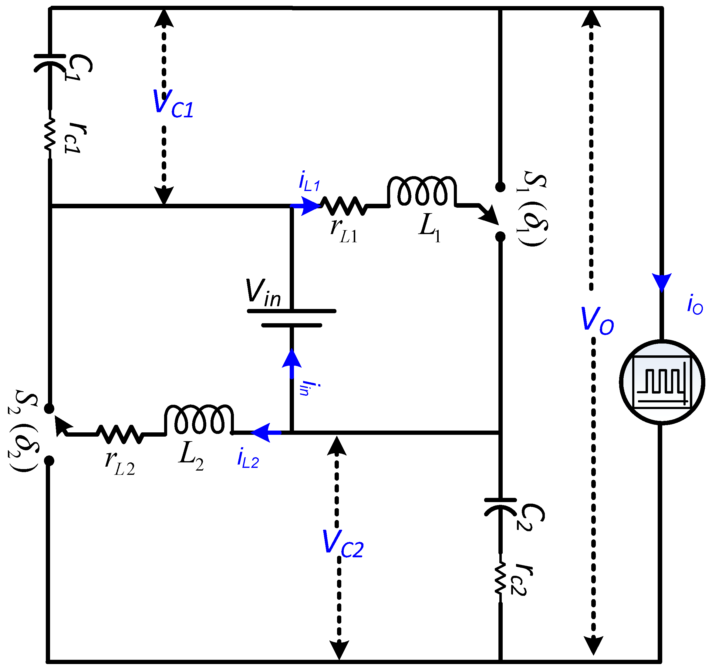
2.1. Topology
2.2. Reduced-Order Mathematical Model of IDCCB
3. Modelling of the N-Phase Converter
Small-Signal State-Space Model
4. Capacitor Voltage Profile
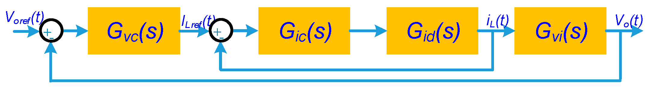
5. Control Design
6. Parameter Variation Effects
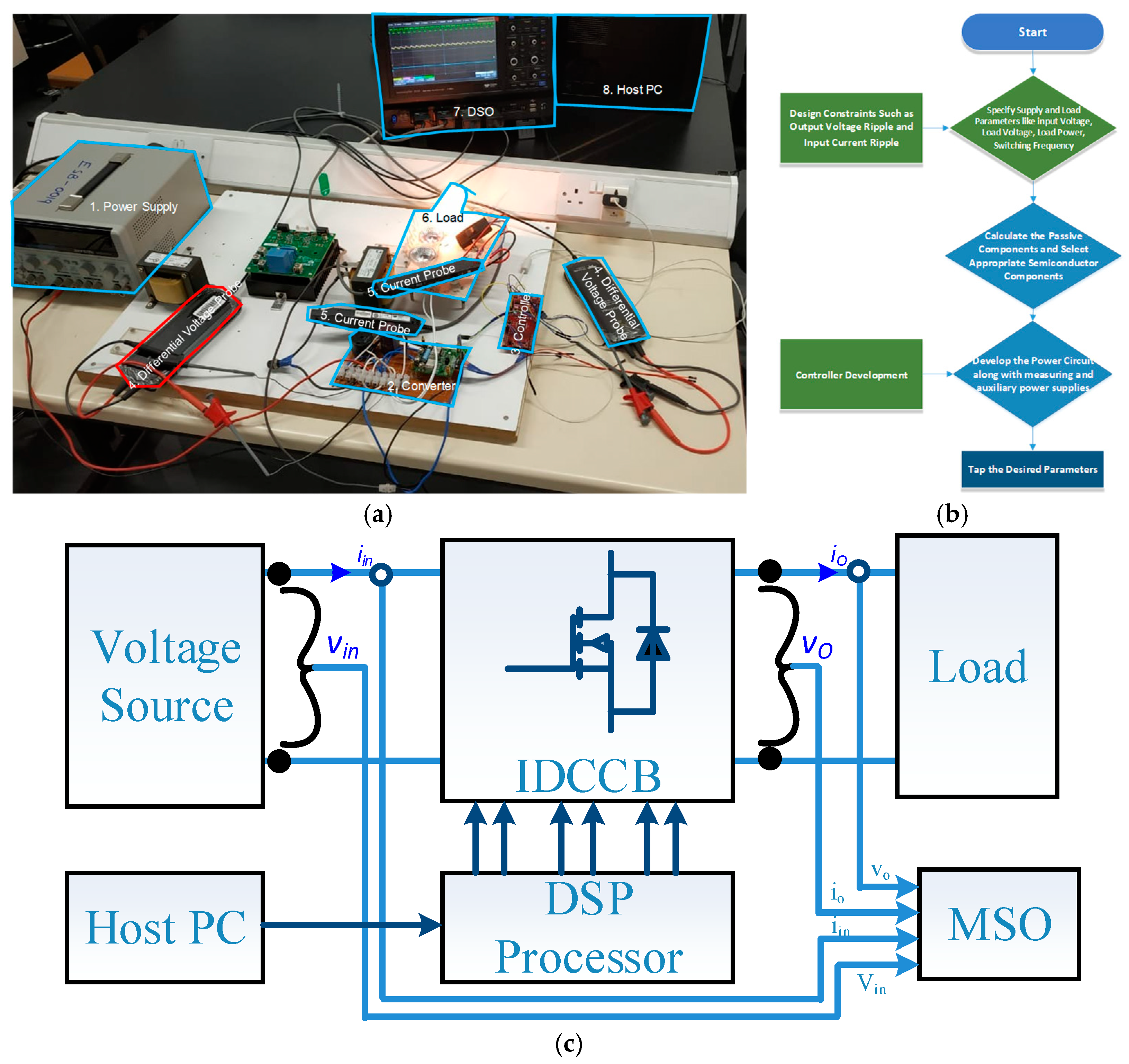
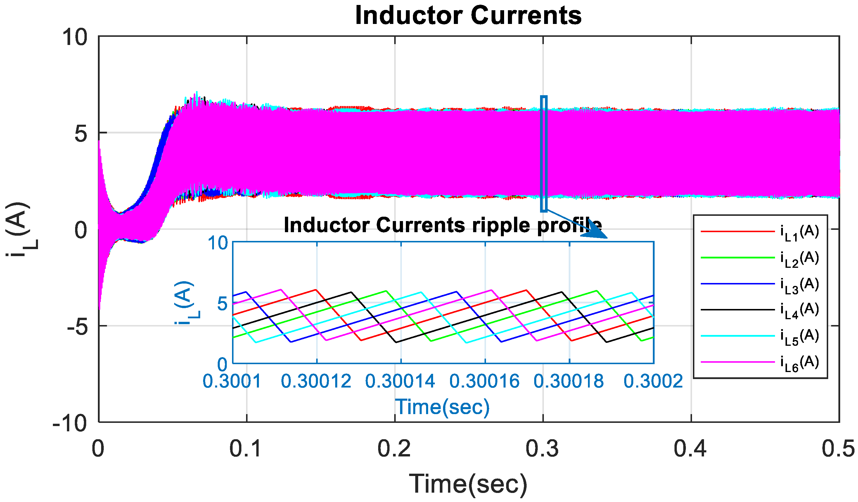
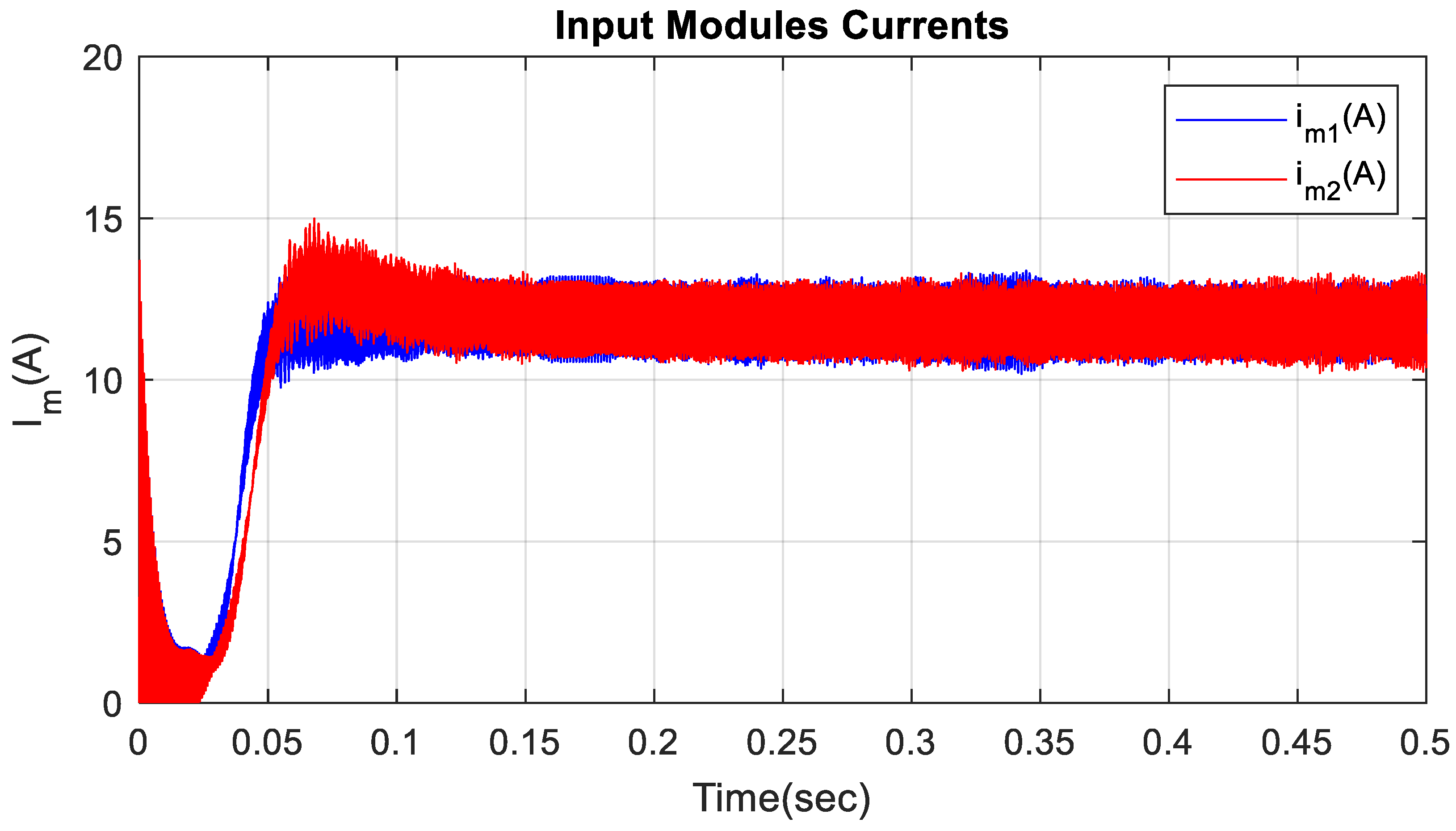
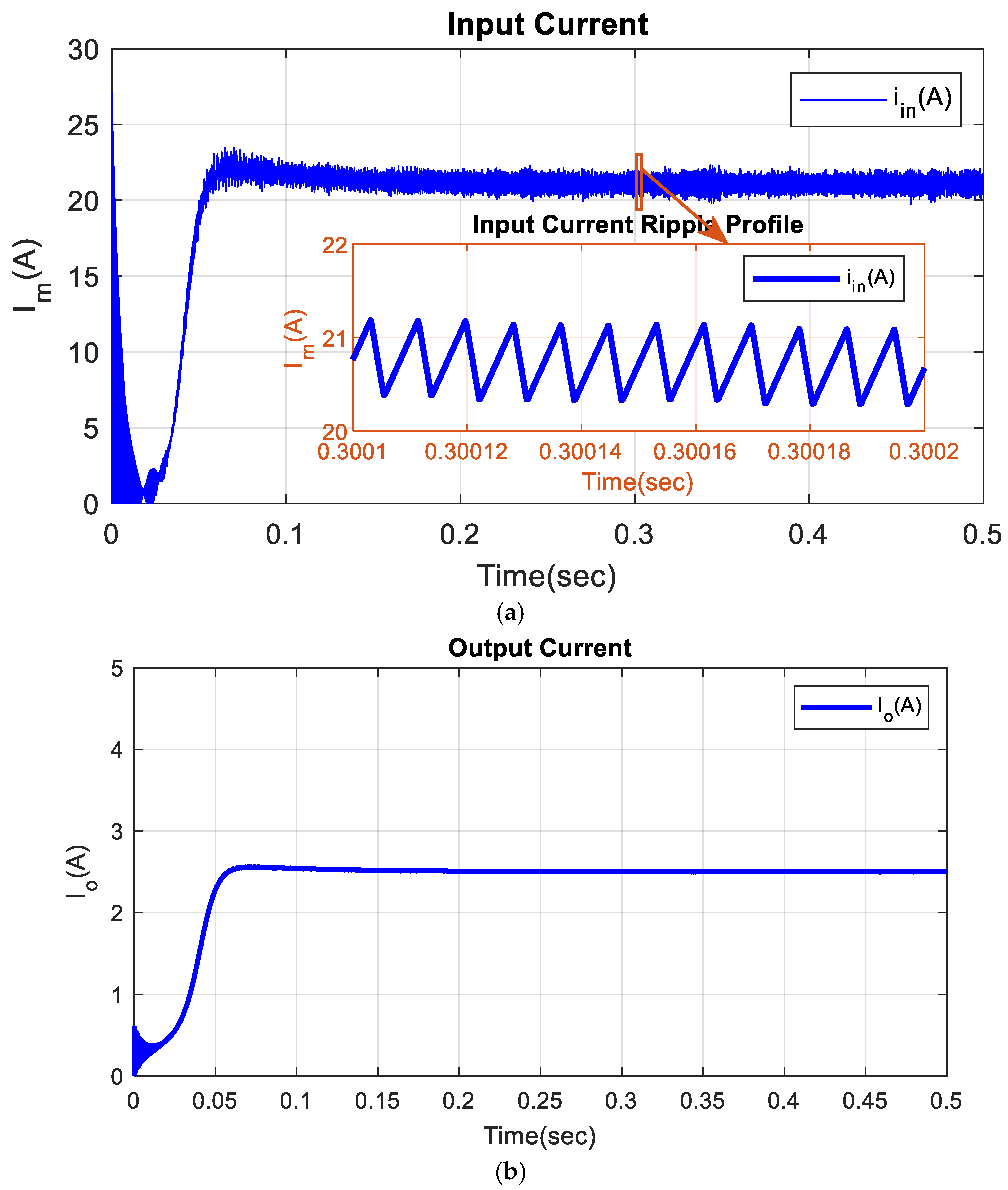
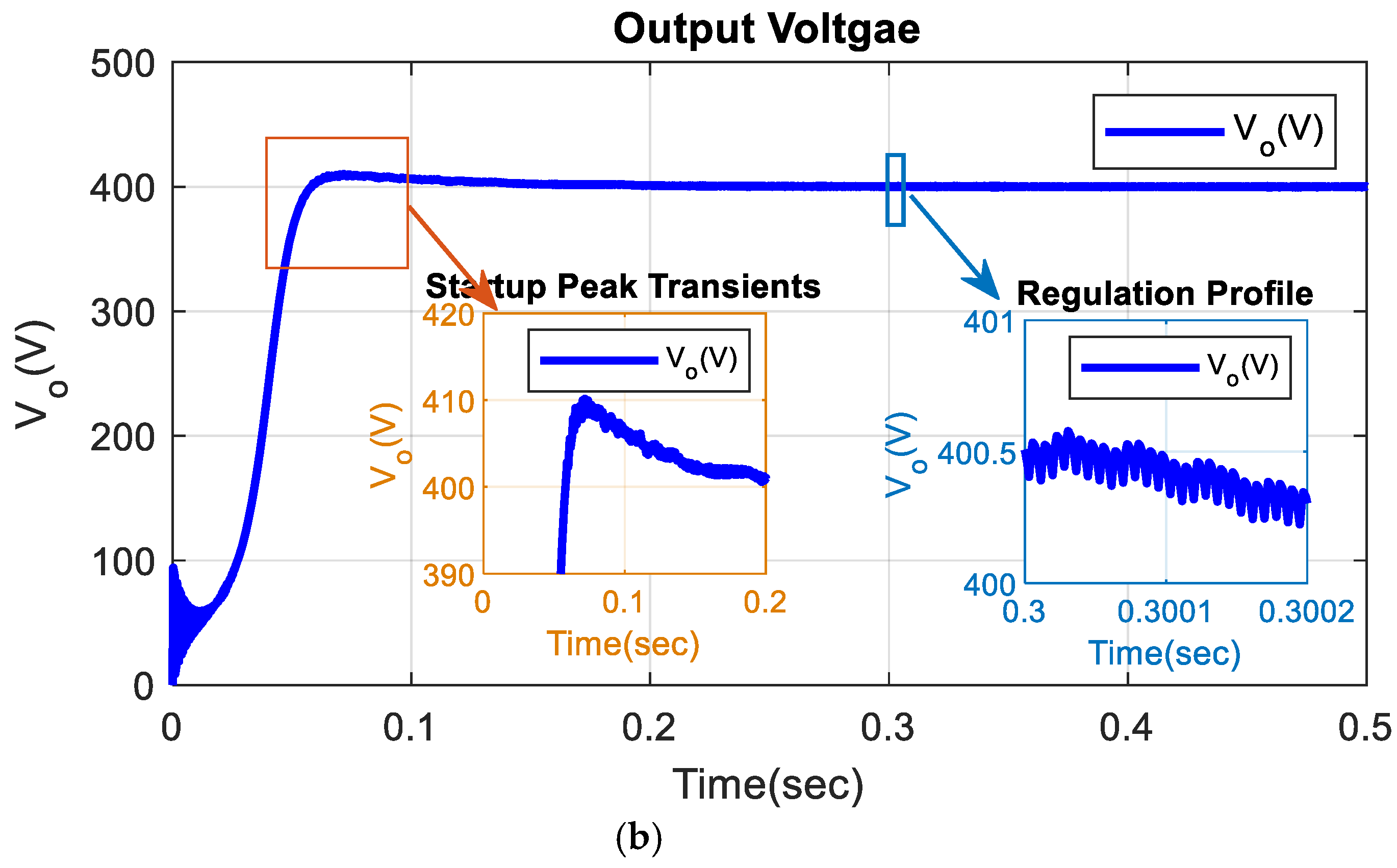
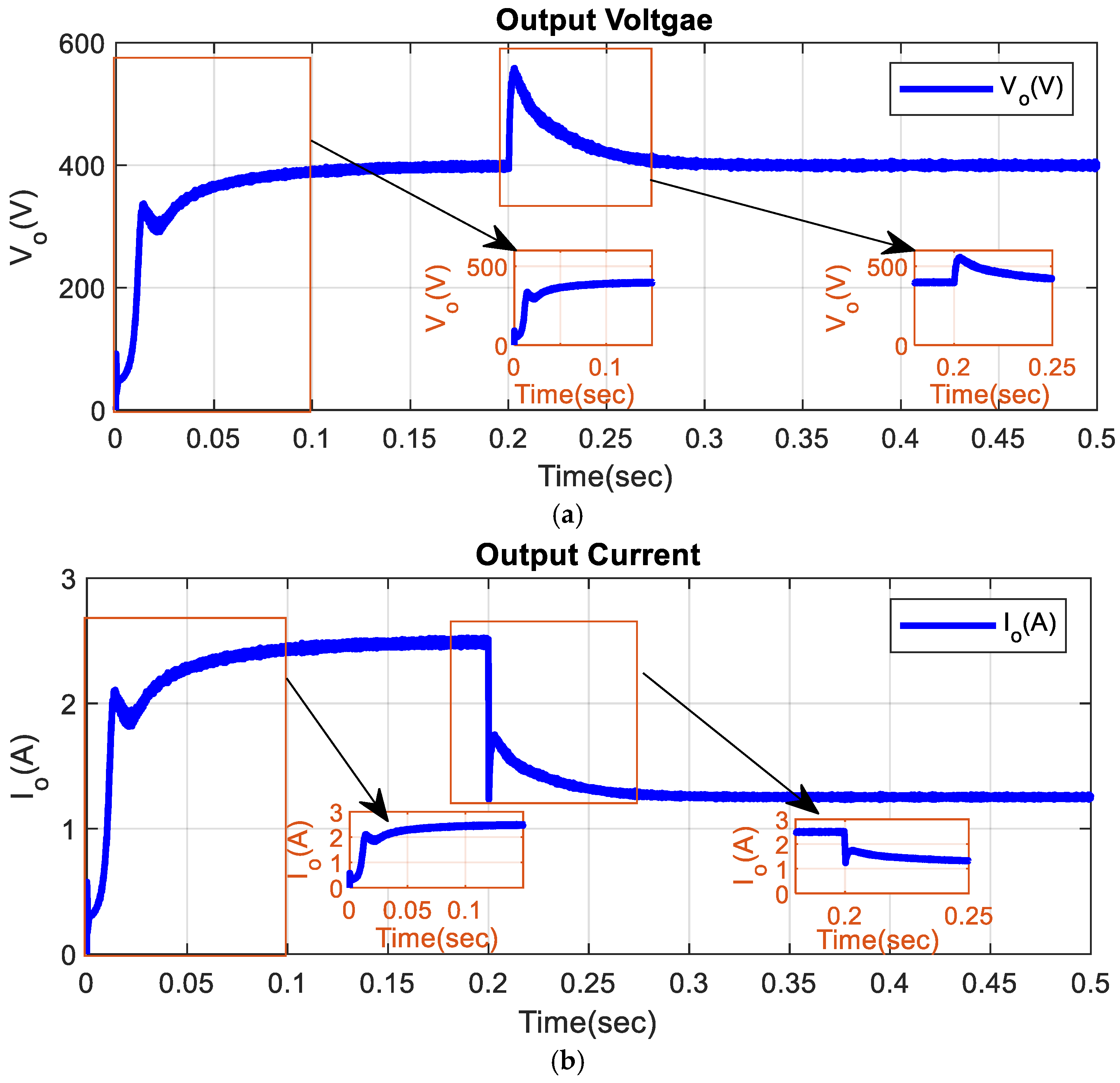
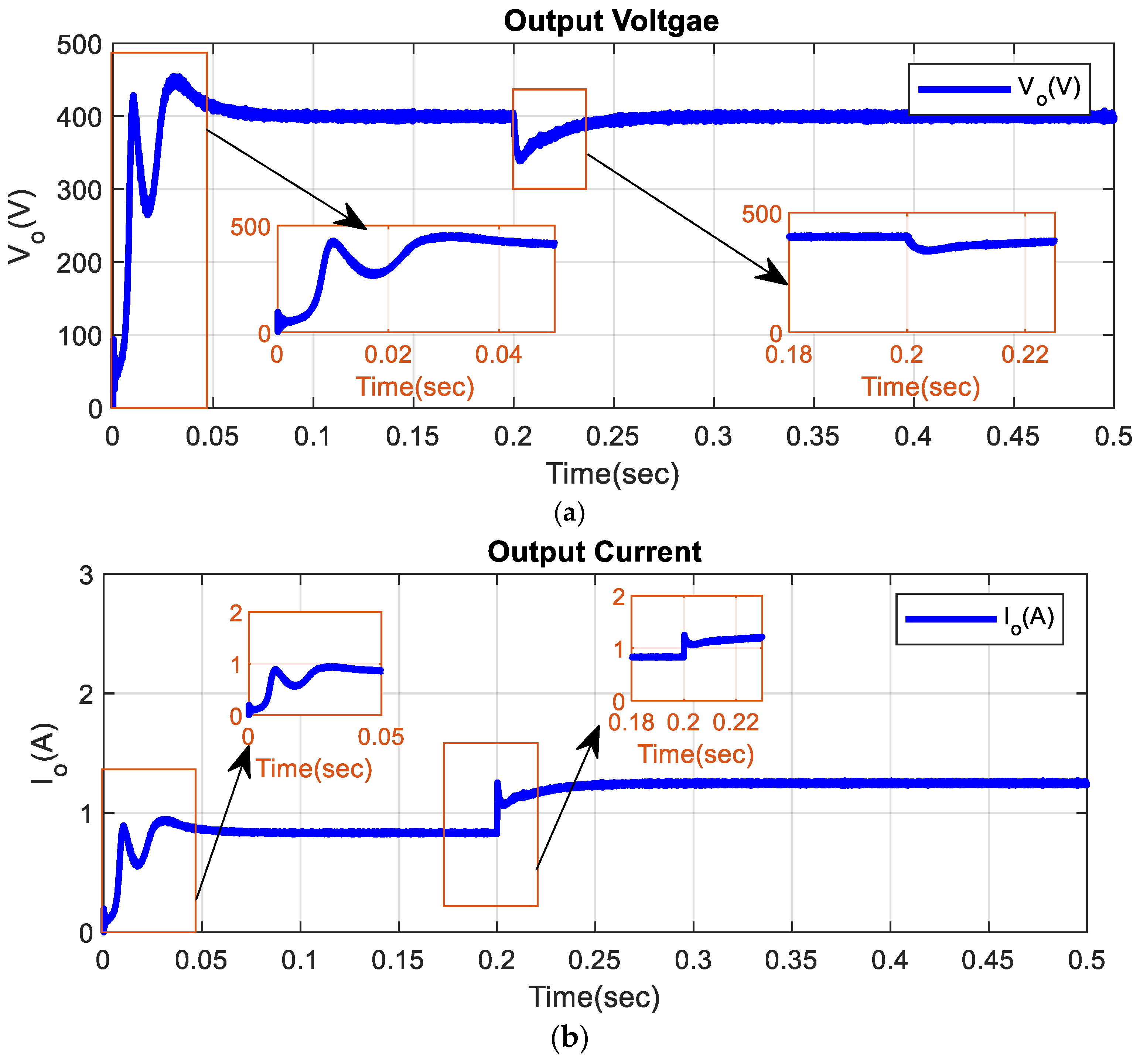
7. Experimental Results
8. Conclusions
Author Contributions
Funding
Institutional Review Board Statement
Informed Consent Statement
Data Availability Statement
Conflicts of Interest
References
- Raveendhra, D.; Praveen, J.; Rajana, P. Mitigation of Electrical Inertia of PE Converters in Solar Powered HESS system for Remote Area Power System Applications using Synergetic Controller. In Proceedings of the 2021 Fourth International Conference on Electrical, Computer and Communication Technologies (ICECCT), Erode, India, 15–17 September 2021; pp. 1–8. [Google Scholar] [CrossRef]
- Chang, Y.-H.; Wu, K.-W. A gain/efficiency-enhanced bidirectional switched-capacitor DC-DC converter. Int. J. Circuit Theory Appl. 2012, 42, 468–493. [Google Scholar] [CrossRef]
- Mukhopadhyay, S.; Takrouri, R.D.; Mohannad, T.; Raveendhra, D. Supercapacitor Characterization Using Universal Adaptive Stabilization and Optimization. IEEE Open J. Ind. Electron. Soc. 2020, 1, 166–183. [Google Scholar] [CrossRef]
- Raveendhra, D.; Thakur, P.; Chauhan, A. FPGA Controlled Power Conditioning System for Solar PV Fed PMDC Motor. In Power Electronics and Renewable Energy Systems. Lecture Notes in Electrical Engineering; Kamalakannan, C., Suresh, L., Dash, S., Panigrahi, B., Eds.; Springer: New Delhi, India, 2015; Volume 326, ISBN 978-81-322-2119-7. [Google Scholar]
- Kseng, K.C.; Kang, J.H.; Tsai, T.H.; Cheng, C.A. Analysis and implementation of a high step-up converter for fuel cell power-generation systems. Int. J. Circuit Theory Appl. 2016, 44, 1814–1827. [Google Scholar]
- Jang, Y.; Jovanovic, M.M. New two-inductor boost-converter with auxiliary transformer. IEEE Trans. Power Electron. 2004, 19, 169–175. [Google Scholar] [CrossRef]
- Javidan, J. Design of a ZVS PWM DC–DC converter for high gain applications. Int. J. Circuit Theory Appl. 2016, 44, 977–995. [Google Scholar] [CrossRef]
- Raveendhra, D.; Pathak, M.K.; Panda, A. Power conditioning system for solar power applications: Closed loop DC-DC convertor fed FPGA controlled diode clamped multilevel inverter. In Proceedings of the 2012 IEEE Students’Conference on Electrical, Electronics and Computer Science, Bhopal, India, 1–2 March 2012; pp. 1–4. [Google Scholar] [CrossRef]
- Chen, Y.T.; Lin, Y.C.; Liang, R.H. An interleaved high step-up DC-DC converter with double boost paths. Int. J. Circuit Theory Appl. 2015, 43, 967–983. [Google Scholar] [CrossRef]
- Babaei, E.; Saadatizadeh, Z. A new interleaved bidirectional dc/dc converter with zero voltage switching and high voltage gain: Analyses, design and simulation. Int. J. Circuit Theory Appl. 2017, 45, 1773–1800. [Google Scholar] [CrossRef]
- Dwari, S.; Jayawant, S.; Beechner, T.; Miller, S.; Mathew, A.; Chen, M.; Riehl, J.; Sun, J. Dynamics characterization of coupled inductor boost dc-dc converters. In Proceedings of the IEEE Workshops on Computers in Power Electronics, Troy, NY, USA, 16–19 July 2006; pp. 264–269. [Google Scholar]
- Narasimharaju, B.L.; Reddy, U.R.; Dogga, R. Design and analysis of voltage clamped bidirectional DC–DC converter for energy storage applications. J. Eng. 2018, 7, 367–374. [Google Scholar] [CrossRef]
- Raveendhra, D.; Dhaouadi, R.; Rehman, H.; Mukhopadhyay, S. LC Impedance Source Bi-Directional Converter with Reduced Capacitor Voltages. Electronics 2020, 9, 1062. [Google Scholar] [CrossRef]
- Radmanesh, H.; Soltanpour, M.R.; Azizkandi, M.E. Design and implementation of an ultra-high voltage DC-DC converter based on coupled inductor with continuous input current for clean energy applications. Int. J. Circ. Theory Appl. 2020, 49, 348–379. [Google Scholar] [CrossRef]
- Raveendhra, D.; Kumar, B.; Mishra, D.; Mankotia, M. Design of FPGA based open circuit voltage MPPT charge controller for solar PV system. In Proceedings of the 2013 International Conference on Circuits, Power and Computing Technologies (ICCPCT), Nagercoil, India, 20–21 March 2013; pp. 523–527. [Google Scholar]
- Garcia, F.S.; Pomilio, J.A.; Spiazzi, G. Modeling and Control Design of the Interleaved Double Dual Boost Converter. IEEE Trans. Ind. Electron. 2013, 60, 3283–3290. [Google Scholar] [CrossRef]
- Garcia, F.S.; Pomilio, J.A.; Spiazzi, G. Modeling and control design of the six-phase Interleaved Double Dual Boost converter. In Proceedings of the 2010 9th IEEE/IAS International Conference on Industry Applications—INDUSCON 2010, Sao Paulo, Brazil, 8–10 November 2010; pp. 1–6. [Google Scholar]
- Mohan, N.; Undeland, T.; Robbins, W.P. Power Electronics Converters, Applications and Design, 3rd ed.; John Wiley & Sons Inc.: Hoboken, NJ, USA, 2003. [Google Scholar]
- Raveendhra, D.; Thakur, P.; Narasimha Raju, B.L. Design and small-signal analysis of solar PV fed FPGA based Closed Loop control Bi-Directional DC-DC converter. In Proceedings of the 2013 International Conference on Circuits, Power and Computing Technologies (ICCPCT), Nagercoil, India, 20–21 March 2013; pp. 283–288. [Google Scholar]
- Dixon, L. Average current mode control of switching power supplies. In Unitrode Power Supply Design Seminar; Texas Instruments: Dallas, TX, USA, 1990. [Google Scholar]
- Erickson, R.; Madigan, M.; Singer, S. Design of a simple high-power-factor rectifier based on the flyback converter. In Proceedings of the IEEE Conference on Applied Power Electronics Conference and Exposition (APEC), Los Angeles, CA, USA, 11–16 March 1990; pp. 792–801. [Google Scholar]
- Yenugula, B.R.; Ur-Rahman, Z. Transformer less high dc-dc converter based on Cockcroft voltage multiplier for photovoltaic application. J. Eng. Appl. Sci. 2018, 13, 5255–5257. [Google Scholar]
- Raveendhra, D.; Pathak, M.K. Three-Phase Capacitor Clamped Boost Inverter. IEEE J. Emerg. Sel. Top. Power Electron. 2018, 7, 1999–2011. [Google Scholar] [CrossRef]
- Nagi Reddy, B.; Pandian, A.; Chandra Sekhar, O.; Rammoorty, M. Design of non-isolated integrated type ac-dc converter with extended voltage gain and high power factor for class-c&d applications. Int. J. Recent Technol. Eng. 2019, 7, 230–236. [Google Scholar]
- Varma, M.P.C.; Mohanta, D.K.; Kumar, K.S.R.; Sastry, V.V.; Ssekhar, O.C. A novel bidirectional dc-dc topology for electric vehicles using psim. In Proceedings of the International Conference on Signal Processing, Communication, Power and Embedded System, SCOPES 2016, Paralakhemundi, India, 3–5 October 2016; pp. 2078–2080. [Google Scholar]
- Raveendhra, D.; Mahdi, M.; Hakim, R.; Dhaouadi, R.; Mukhopadhyay, S.; Qaddoumi, N. Wireless Charging of an Autonomous Drone. In Proceedings of the 6th International Conference on Electric Power and Energy Conversion Systems (EPECS-2020), Istanbul, Turkey, 5–7 October 2020. [Google Scholar]
- Wenzhi, S.; Zhang, H.; Tseng, M.-L.; Weipeng, Z.; Xinyang, L. Hierarchical energy optimization management of active distribution network with multi-microgrid system. J. Ind. Prod. Eng. 2021, 1–20. [Google Scholar] [CrossRef]
- Li, L.; Wen, S.; Tseng, M.L.; Chiu, A.S.F. Photovoltaic array prediction on short-term output power method in centralized power generation system. Ann. Oper. Res. 2020, 290, 243–263. [Google Scholar] [CrossRef]


| Parameter Name | CCB Module |
|---|---|
| Input voltage, Vin | 48 V |
| Output voltage, Vo | 224 V |
| Duty ratio | 0.7857 |
| Load power | 1000 W |
| Output current, A | 2.5 A |
| Load resistance, Ω | 89.6 Ω |
| Inductor current, A | 11.666 A |
| Output voltage ripple, % | ≤0.5 |
| Switching frequency, kHz | 20 |
| Inductor | 0.5 mH |
| Filter capacitors |
| Parameter | Proposed |
|---|---|
| Duty ratio (D) | 0.7857 |
| Inductor equilibrium current (A) | 11.66 A |
| Capacitor equilibrium voltage (V) | 224 V |
Publisher’s Note: MDPI stays neutral with regard to jurisdictional claims in published maps and institutional affiliations. |
© 2022 by the authors. Licensee MDPI, Basel, Switzerland. This article is an open access article distributed under the terms and conditions of the Creative Commons Attribution (CC BY) license (https://creativecommons.org/licenses/by/4.0/).
Share and Cite
Raveendhra, D.; Rajana, P.; Kumar, K.S.R.; Jugge, P.; Devarapalli, R.; Rusu, E.; Fayek, H.H. A High-Gain Multiphase Interleaved Differential Capacitor Clamped Boost Converter. Electronics 2022, 11, 264. https://doi.org/10.3390/electronics11020264
Raveendhra D, Rajana P, Kumar KSR, Jugge P, Devarapalli R, Rusu E, Fayek HH. A High-Gain Multiphase Interleaved Differential Capacitor Clamped Boost Converter. Electronics. 2022; 11(2):264. https://doi.org/10.3390/electronics11020264
Chicago/Turabian StyleRaveendhra, Dogga, Poojitha Rajana, Kalamchety Srinivasa Ravi Kumar, Praveen Jugge, Ramesh Devarapalli, Eugen Rusu, and Hady H. Fayek. 2022. "A High-Gain Multiphase Interleaved Differential Capacitor Clamped Boost Converter" Electronics 11, no. 2: 264. https://doi.org/10.3390/electronics11020264