Abstract
Systolic arrays are the primary part of modern deep learning accelerators and are being used widely in real-life applications such as self-driving cars. This paper presents a novel factored systolic array, where the carry propagation adder for accumulation and the rounding logic are extracted out from each processing element, which reduces the area, power and delay of the processing elements substantially. The factoring is performed in the column-wise manner and the cost of the factored logic, placed at each column output, is amortized by the processing elements in a column. We demonstrate the proposed factoring in an open source systolic array, Gemmini. The factoring technique does not change the functionality of the base design and is transparent to applications. We show that the proposed technique leads to substantial reduction in area and delay up to 45.3% and 23.7%, respectively, compared to the Gemmini baseline.
1. Introduction
Recently, machine learning (ML) algorithms have acquired considerable attention after deep learning (DL) demonstrated breakthroughs in various complex tasks such as the ImageNet challenge. The vigorous ability of DL to solve complex tasks is not limited to image recognition but also applicable in object detection, speech recognition, natural language processing, etc. [1,2,3]. However, deep learning models require massive amounts of computation and large memory footprints, and recent research have focused on DL accelerators [4]. The matrix multiplication is the key primitive in computation of ML models, and systolic arrays (SAs) for the matrix multiplication have been adopted widely [5,6]. Systolic arrays, proposed in 1979, are two dimensional mesh that consist of processing elements (PEs) organized in the form of a grid [7,8]. Due to data reusability, concurrency and simple architectural characteristics, many industry giants such as Google [9], Nvidia [10], Intel [11] and Samsung [12] utilized systolic array for general matrix multiplication (GEMM). With the increasing interest in accelerators, many studies have been proposed using systolic arrays [9,10,11,12,13,14,15,16], but to the best of our knowledge, all of them focus on dataflows to increase memory bandwidth efficiency and maximum data reuse, etc.; none of them deal with the logic level design of the systolic arrays. In this paper, we present a novel factored systolic array and demonstrate it using an open-source (https://github.com/ucb-bar/gemmini) systolic array, the Gemmini (Gemmini system on chip (SoC) RTL can be generated by following this lab, EE-290-2, Hardware for Machine Learning, Lab-2) [17]. The main contributions of this paper are outlined below:
- We present a novel factored systolic array, referred to as the carry-propagate-adder (CPA)-factored systolic array.
- Using the practical systolic array baseline, we demonstrate that significant improvements in key design metrics are possible without modifying the functionality of the systolic array.
2. Related Works
Early systolic array architectures were used to compute convolutions and GEMMs [9,13,14,15,16]. Detailed survey on ML accelerators is available in [18,19,20,21]. Researchers in academia have proposed many modern SA architectures and we categorize them into the following three types:
2.1. Fixed ML Accelerator Designs
Due to incredible amount of interest in machine learning accelerators, the architecture community has focused on designing efficient dataflows to maximize the operand reuse and unnecessary data transfer in [22,23] for Convolutional Neural Networks (CNN). In [22], the authors implemented indexed based Sparse CNN (SCNN) accelerator architecture to improve the energy efficiency. However, indexed based approaches have significant overhead costs for storing and computing on the indexes. In [23] Liu et al. introduced density bound block (DBB) to make the bound on the number of non-zero elements in each block to deal with the sparse data and sparsity is fixed at the design time in their scheme. Unfortunately, with fixed sparsity any models that do not achieve or exceed this threshold must fall back to dense operation with no benefit.
2.2. Flexible ML Accelerator Designs
To support a variety of workloads, flexible mapping by supporting multiple dataflows has been proposed in ML accelerators [24,25,26]. In these studies, refs. [24,25] flexible accelerators are natively designed for convolution to support data reusability. However, ref. [26] introduces FlexSA, a flexible systolic array architecture for GEMMs operation, which dynamically re-configures the systolic structure. Indeed, flexibility is good for pruned or sparse CNN accelerators but this flexibility increases implementation cost due to increment in data traffic in accelerators and extra control logic. This is acceptable for small convolution/matrix computation but it severely increases the cost for large GEMMs.
2.3. Logic Level ML Accelerator Designs
Since the processing element and systolic array are the main components of ML accelerators, some recent works proposed the re-architecting of these components at the logic level [27,28], respectively. In [27], the Tetris accelerator was proposed that not only deal with sparsity but also with zero bits in non-zero values through split-and-accumulate (SAC) unit in PEs to increase the efficiency in accelerator. Tetris is good for small matrix tiles but does not have enough computation power to work on larger networks without multiple costly passes due to increment in complex control logic. In [28], Ullah et al. proposed a factored radix-8 systolic array, in which differently sized SAs have been implemented and suggested to perform extraction of radix-8 multiplier booth encoding and hard multiple computation of multiplicand Y as a pre-processing at the input of systolic array. It also demonstrated the substantial improvements in 16 bit or higher systolic arrays, but showed less improvements in 8 bit or lower SAs, which are typically used for inference acceleration in edge devices.
In the above discussed previous work, much of the focus on ML accelerator design has been on optimizing core dataflows to improve local reuse of data and reduce expensive data movement between the processing elements, increase memory bandwidth efficiency, etc. Thus, critically, the logic-level design of datapath components needs more attention.
We target the systolic array accelerator at logic level without adding control logic complexities and proposed novel CPA-Factored Gemmini Systolic Array which provides same functionality as the conventional systolic array and achieves significant improvements in the area and delay.
3. Proposed Design
3.1. CPA-Factored Systolic Array
We consider a 2-dimensional (2-D) systolic array where PEs are organized in the form of a mesh grid. Each PE receives two inputs A and B and utilize multiplication and accumulation (MAC) to perform the multiplication and accumulation on every clock cycle. Let . Also, let denote the partial sum stored in the accumulator register. The multiplier in a PE is usually considered as a black-box primitive.
However, we consider the logic-level design of the multiplier here. Initially, the multiplier performs partial product (PP) generation and partial product reduction in the reduction tree. Then, it performs final addition using a carry propagation adder (CPA), and the multiplier output X is added to using another CPA. To avoid accuracy degradation, systolic arrays for machine learning usually deploys a CPA with a high bit-width (e.g., 32 bit instead of 8 bit or 16 bit), which causes significant delay and area overhead in MAC computation. In systolic arrays, we can replace them with two Carry Save Adders (CSAs) for the accumulation and place a CPA in each column output of the array for the final addition.
A CSA is a 3:2 compressor, while reducing three inputs to two, does not propagate carry; it rather keeps the carry (shift carry) in the next significant bit position with partial sum (also known as pseudo sum), these two values are known as a redundant binary representation [29,30]. For the delay and area perspective, the delay of CSA is a constant with respect to the word-length and the area of CSA is linear. Thus, the PE delay, which is often the critical path delay of the whole SA, and the PE area can be reduced significantly. In addition, the area cost of the factored CPA can be amortized by PEs in a column and becomes marginal as the size of the array increases. We refer to this structure as the CPA-factored systolic array. However, this factoring will cause a double sequential area in each PE because, in this case, we need to store two values (the sum and carry vectors) in two accumulator registers (, ) instead of one, as shown in Figure 1b.
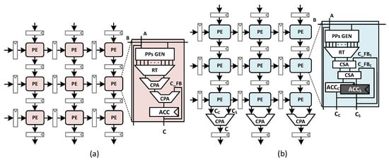
Figure 1.
(a) Conventional systolic array (SA) architecture (i.e., Gemmini SA). (b) Proposed carry propagation adder (CPA)-factored systolic array architecture. The systolic architecture with the output stationary dataflow allows us to store the partial sum in a PE in the carry save representation and to convert it into the binary form at the column output.
Moreover, every PE propagates these two values downwards. Thus, the pipeline register cost for output migration in the systolic array is also doubled. However, this increment in sequential cost can be compensated by simplifying the logic in PEs.
3.2. Gemmini Systolic Array Architecture
Gemmini [17] is an open source generator of systolic array accelerators that supports multiple data flows for application-specific integrated circuits (ASICs) and field programmable gate arrays (FPGAs) implementation. We considered a Gemmini systolic array with output stationary data flow as shown in Figure 2 that performs all the computation on 8 bit signed inputs. This Gemmini SA consists of a set of PEs interconnected as a 2-D array. Pipeline registers are placed in the input and output of PEs in such a way that all PEs communicate only adjacent with nominal data migration and high computational parallelism in a wave-front flow. Input matrices A, B and D are provided at the left edge and the top edge of the systolic array to perform the GEMM through PEs as represented by the equation:
where A and B are the multiplied matrices, C is the result and D is accumulator preload (bias matrix) in output stationary dataflow. This architecture is a practical version of previously discussed proposed systolic array shown in Figure 1a. The Gemmini systolic array MAC contains an 8 bit signed multiplier for multiplication and 32 bit adder (CPA) for accumulation. Accumulation is performed with 32 bits to avoid accuracy degradation in machine learning. Some components (double buffer and peripheral logic (PL)) are different than Figure 1a because original Gemmini SA supports the full utilization of MAC and rounding (e.g., PL circuitry is to truncate the final output 32 bit into 16 or 8 bit etc.) on final output. To enable non-stop MAC (or full utilization of MAC) computation, each PE exploits the double buffer so that inputs can be loaded for future computation or previous results can be propagated at output of systolic array while the current compute cycle is running.
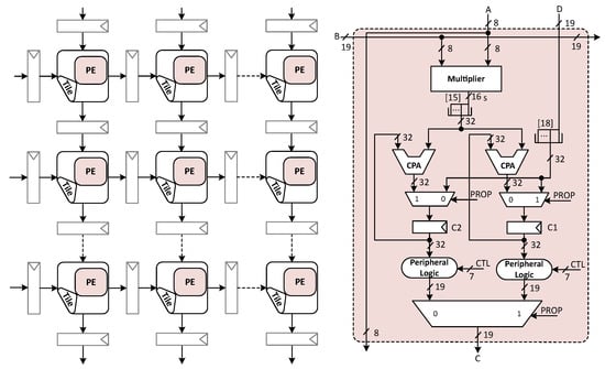
Figure 2.
Gemmini systolic array architecture with output stationary dataflow.
To reduce the critical path delay, it has two accumulation registers and two dedicated datapaths, one for each register. Thus, each register has a separate accumulator (CPA) and a peripheral logic for accumulation, as shown in Figure 2. To select the input and outputs for computation and propagation Gemmini systolic array double buffer has two multiplexers (2:1 MUX) at input, one big multiplexer (MUX) (2:1 MUX) at output; these multiplexers are driven by one bit propagation (PROP) select line.
3.3. CPA-Factored Gemmini Systolic Array Architecture
The architecture of the proposed CPA-factored Gemmini systolic array with output stationary dataflow is shown in Figure 3 that also perform all computation on 8 bit signed inputs. In this architecture, for MAC, we utilize the radix-4 signed multiplier (we adopted the multiplier design from [31]) and we represent the partial sum in a PE in the carry save representation and use two carry save adders for accumulation. Thus, we can remove all the CPAs from the PE in Gemmini. As mentioned before, the CSAs provide binary redundant representation that contain two values (partial sum and shift carry); therefore, in the proposed Gemmini systolic array architecture, the double buffer has four registers to accommodate four values (two values for computation and two values for propagation). To get the final value, we place a CPA column-wise at the output of the array to add the partial sum and shift carry values. The PL circuitry rounds the final dot-product from a high bit-width down to a lower bit-width.
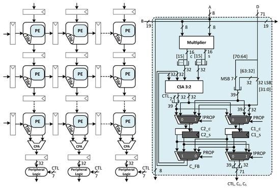
Figure 3.
CPA-Factored Gemmini systolic array architecture with output stationary dataflow.
However, because we factor out the final addition outside PEs column-wise, it is not reasonable to deploy this PL circuitry inside PE. Thus, we factor out the PL circuitry from all PEs and place it next to the CPA in each column with the small cost of an additional 7 bit register for the control line CTL (five SHIFT bit, one ENABLE and one PROP) in PE and 7 bits increment in pipeline registers of systolic array. However, the overall incremented sequential cost is further offset by removing redundant hardware, which is explained in the coming section.
3.4. Double Buffer Complexities in Systolic Arrays
As mentioned earlier, the Gemmini SA double buffer has two datapaths, that is basically to remove the multiplexer delay from the critical path of the accumulator, but it also creates a redundancy in the hardware and this redundant hardware is replicated across all PEs in the systolic array, increasing the overall area of the systolic array significantly. However, the proposed CPA-factored Gemmini systolic array exploit the double buffer, which has two dedicated outputs (one for accumulator computation and one for output propagation) and a common accumulator (CSAs) inside PE. This helps to remove the redundant adder and factor out a common PL circuitry. In this way, the CPA-factored Gemmini systolic array offsets the aforementioned effect of sequential area growth in the total area. The proposed SA double buffer has two multiplexers at input and two multiplexers at output, adding a multiplexer delay in the MAC critical path but our MAC design can accommodate this as we already eliminated the CPA delay in the MAC critical path.
4. Evaluation and Analysis
4.1. Evaluation Setup and Baseline
In this work, our baseline is Gemmini generated output stationary SA architecture with 32 bit accumulator word-length (acc. WL). Therefore, we compared the the proposed PE and SA designs with the Gemmini designs. We also analyzed the proposed PE and SA designs in comparison to the Gemmini PE and SA designs at different accumulator word-lengths (16, 32 and 64 acc. WL). All the designs were implemented in Verilog and verified using Synopsys VCS. For verification, we built the test binaries using bare-metal software (Bare-metal software given in the Gemmini open source repository) test and checked the correctness of both designs in bare-metal environment. Moreover, an industrial 32 nm standard cell library was used to map the designs and was synthesized by the Synopsys Design Compiler. For the power measurements, PrimePower was used. The first switching activity interchange format (SAIF) file was generated by post processing the gate-level simulation using random input vectors in VCS; then, power dissipation was acquired by annotating the SAIF file to the netlist. All experiments were performed on a Linux machine.
4.2. Comparison of Systolic Array with 32 Acc. WL
4.2.1. Processing Element
The comparison of PE area, delay, power, power delay product (PDP) and area delay product (ADP) is shown in Table 1. Even though the binary redundant representation and the forwarded control signals added the register cost in the proposed PE as compared to the baseline, the baseline Gemmini systolic array’s PE total area is still higher compared to the proposed SA’s PE. Similarly, as in the proposed CPA-factored Gemmini SA, we used two CSAs instead two CPAs and removed the CPA completely from the PE, on average the total delay is also improved.

Table 1.
Implementation results for Gemmini [17] and the proposed CPA-Factored Gemmini processing elements (PEs).
However, since the sequential area is more than double in the proposed design due to redundant representation and the control signal, the power gets degraded slightly as compared to Gemmini designs. Overall the proposed PE shows improvement in all the key metrics over the baseline except power and have been normalized with respect to the baseline as shown in the Figure 4 (left). It can be seen that the area and delay of the proposed PE are 44.1%, 16.9% less than those of the Gemmini systolic array PE, respectively. The PDP and ADP are also improved by 6.1% (improvement in PDP is not significant due to the power degradation) and 53.5% as compared to Gemmini PE, respectively.
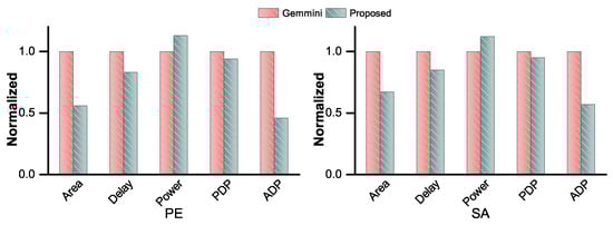
Figure 4.
Performance comparison of proposed CPA-Factored Gemmini PE, SA and baseline Gemmini PE, SA.
4.2.2. Systolic Arrays
The performance comparison of CPA-factored Gemmini SA area, delay, power, PDP and ADP is shown in Table 2 with baseline Gemmini SA. The additional bits we stored in PE cost in the systolic array as well, because we have pipeline registers at input and output of each PE to keep data migration in wave-front flow. However, at the same time, the factorization of CPAs, peripheral circuitry and modified double buffer not only balance out the aforementioned sequential area cost by removing the combinational area but also reduce the total area significantly in the proposed systolic array as compared to the baseline Gemmini systolic array.
Table 2.
Implementation results for 8 × 8 Gemmini [17] and proposed CPA-Factored Gemmini systolic arrays (SAs).
The area and delay of CPA-Factored Gemmini SA are 33.3% and 14.9% less than those of Gemmini SA, respectively (the proposed SAs evaluation normalized metrics are shown in Figure 4 (right) to those of corresponding baseline for the comparison). Moreover, the PDP and ADP performance of proposed SA is 4.7% and 43.1% better than those of the baseline, respectively.
4.3. Comparison of Different Acc. WL Systolic Arrays
We also compared the proposed design of PEs and SAs with different acc. WLs according to all key metrics (area, delay, etc) with Gemmini designs in Table 3. In the PEs, due to the proposed CPA factoring, the combinational area improvement increases as the acc. WL increases, but the delay improvement remains stable (as now there is no carry propagation in the PE design: thus, this improvement is stable with the accumulator length.) because of CSAs.
Table 3.
Implementation results for 16, 32 and 64-bit accumulator word-length (acc. WL) Gemmini and proposed CPA-Factored Gemmini SAs.
For SAs, Figure 5 breaks the combinational and sequntial area down for insight comparison with the delay. It can be seen that the reduction in the SA combinational area and delay (26.9–68%, 14.7–23.7%, respectively) significantly increases as the acc. WL increases and correspondingly, the degradation in sequential area is not significant. Thus, it reduces the total area (7.1–45.3%) in the proposed SAs too as the acc. WL increases. Moreover, the PDP and ADP performance of the proposed SAs is up to 31.9% and 58.2% better than those of baseline, respectively.
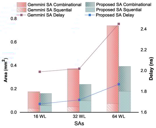
Figure 5.
Delay, combinational area and sequantial area comparison of different accumulator wordlength (acc. WL) proposed CPA-Factored Gemmini systolic arrays (SAs) and baseline SAs.
5. Discussion
CPA-factored Gemmini SA focuses its whole systolic array design at the logic level on improving the overall area and the delay for machine learning accelerators, which is very different from the direction taken in many of the previous state-of-the-art works.
Broadly speaking, the architecture community has focused on exploring of possible dataflows by exploiting model sparsity and model pruning, etc., and proposed fixed or flexible machine learning accelerators. All of these works are highly relevant to this field but do have some limitations: First, most of these ML accelerators use convolutional neural networks (CNNs) and few mentioned other neural networks (NNs). Unfortunately, according to Google, CNN utilization in data center NNs is barely 5% and mostly utilized in edge devices [9]. Second, fixed or flexible ML accelerators both work well with small scale convolution/matrix computation but for large GEMMs computation, design complexities increase, such as threshold match, huge data communication and additional control logic.
For large GEMMs, Google introduced the first tensor processing unit (TPUv1) in [9], which used an 8-bit integer systolic array to accelerate the inference and to replace general purpose computing units such as GPUs/CPUs in data centers. In TPUv1, the main architecture feature was the systolic array, which reduces the area and power of the large matrix multiplication unit. However, the MAC of TPUv1 (and many other ML accelerators including Gemmini) utilize conventional components (e.g., multipliers and adders). Recently, ref. [28] proposed the factored systolic array (FSA) using the radix-8 multiplier, in which the authors adopted non-conventional approach by considering systolic array and multiplier together and factored out the booth encoding and hard multiple (3Y) as a pre-processing unit. However, it is worth noting that the systolic array (either radix-4 or radix-8 multiplier) delay and area complexity mainly lies on the MAC accumulation feedback. The carry propagate adder is the main bottleneck in this feedback as it adds a huge delay due to the carry propagation. Thus, this delay increases as the accumulator word-length increases.
Therefore, in this paper we suggested considering systolic array and computing components multiplier and adders all together (unlike [28], which considered only SA and multiplier). We demonstrated the idea of performing accumulation using CSAs inside PE in binary redundant form and factoring out the CPA from PE and placed column-wise in SA for the final addition to get the final output. We have seen that this simple proposed technique leads to a substantial reduction in the area and delay.
Since the proposed design gained significant improvement in the area and delay, it can be useful in data centers or for the cloud: whether in training or inferences as in both cases area and delay constraints applies to accelerators.
6. Conclusions
This work presented a novel systolic array based on CPA and rounding logic factoring, and demonstrated that the proposed CPA-Factored SA can substantially ameliorate the area and delay. This factoring is done at the cost of an increased number of registers in the processing elements and systolic arrays, which cause power degradation. However, the growth in sequential area is compensated for by reducing the double buffer complexities and removing the redundant hardware. Compared with the baseline Gemmini SA design equipped, the CPA-Factored Gemmini SA achieved significant improvements in area and delay. Moreover, we have also shown that, for high precision cases when acc. WL increases, the reduction in area and delay also increases substantially when compared to the baseline.
Consequently, this paper provides substantial evidence of the critical importance of the reconsideration in the design path of arithmetic components for machine learning accelerators. For future research, we believe more exploration is required in that research path to enable these designs to work on low-powered edge devices, which may be our future work.
Author Contributions
Conceptualization, J.C.; data curation, K.I.; formal analysis, K.I. and J.C.; funding acquisition, J.C.; investigation, K.I. and J.C.; methodology, K.I. and J.C.; project administration, J.C.; software, K.I.; supervision, J.C.; validation, K.I. and J.C.; writing—original draft, K.I.; writing—review and editing, J.C. All authors have read and agreed to the published version of the manuscript.
Funding
This work was supported by Samsung Research Funding & Incubation Center of Samsung Electronics under Project Number SRFC-TB1803-02.
Conflicts of Interest
The authors declare no conflict of interest.
Abbreviations
The following abbreviations are used in this manuscript:
| ML | Machine Learning |
| DL | Deep Learning |
| GEMM | General Matrix Multiplication |
| CNN | Convolutional Neural Network |
| MAC | Multiplication and Accumulation |
| SAC | Split-and-Accumulate |
| PP | Partial Product |
| CPA | Carry Propagate Adder |
| CSA | Carry Save Adder |
| SA | Systolic Array |
| PE | Processing Element |
| ADP | Area Delay Product |
| PDP | Power Delay Product |
References
- Qin, E.; Samajdar, A.; Kwon, H.; Nadella, V.; Srinivasan, S.; Das, D.; Kaul, B.; Krishna, T. SIGMA: A sparse and irregular gemm accelerator with flexible interconnects for dnn training. In Proceedings of the IEEE International Symposium on High Performance Computer Architecture (HPCA), San Diego, CA, USA, 22–26 February 2020; pp. 58–70. [Google Scholar]
- Hegde, K.; Yu, J.; Agrawal, R.; Yan, M.; Pellauer, M.; Fletcher, C. UCNN: Exploiting computational reuse in deep neural networks via weight repetition. In Proceedings of the ACM/IEEE 45th Annual International Symposium on Computer Architecture (ISCA), Los Angeles, CA, USA, 1–6 June 2018; pp. 674–687. [Google Scholar]
- Silver, D.; Schrittwieser, J.; Simonyan, K.; Antonoglou, I.; Huang, A.; Guez, A.; Hubert, T.; Baker, L.; Lai, M.; Bolton, A.; et al. Mastering the game of go without human knowledge. Nature 2017, 550, 354–359. [Google Scholar] [CrossRef] [PubMed]
- Sze, V.; Chen, Y.H.; Yang, T.J.; Emer, J.S. Efficient Processing of Deep NEURAL networks; Synthesis Lectures on Computer Architecture; Morgan and Claypool Publishers: San Rafael, CA, USA, 2020; Volume 15, pp. 1–341. [Google Scholar]
- Sze, V.; Chen, Y.H.; Yang, T.J.; Emer, J.S. Efficient processing of deep neural networks: A tutorial and survey. Proc. IEEE 2017, 105, 2295–2329. [Google Scholar] [CrossRef]
- Kwon, H.; Chatarasi, P.; Pellauer, M.; Parashar, A.; Sarkar, V.; Krishna, T. Understanding reuse, performance, and hardware cost of dnn dataflow: A data-centric approach. In Proceedings of the 52nd Annual IEEE/ACM International Symposium on Microarchitecture, Columbus, OH, USA, 12–16 October 2019; pp. 754–768. [Google Scholar]
- Kung, H.T.; Leiserson, C.E. Algorithms for VLSI processor arrays/eds. In Introduction to VLSI Systems; Mead, C., Conway, L., Eds.; Addison-Wesley: Boston, MA, USA, 1979. [Google Scholar]
- Gentleman, W.M.; Kung, H.T. Matrix triangularization by systolic arrays. In Real-Time Signal Processing IV; International Society for Optics and Photonics: Bellingham, DC, USA, 1982; Volume 298, pp. 19–26. [Google Scholar]
- Jouppi, N.P.; Young, C.; Patil, N.; Patterson, D.; Agrawal, G.; Bajwa, R.; Bates, S.; Bhatia, S.; Boden, N.; Borchers, A.; et al. In-datacenter performance analysis of a tensor processing unit. In Proceedings of the 44th Annual International Symposium on Computer Architecture, Toronto, ON, Canada, 24–28 June 2017; pp. 1–12. [Google Scholar]
- NVIDIA. Nvidia Turing Gpu Architecture; NVIDIA: Santa Clara, CA, USA, 2019. [Google Scholar]
- Cyphers, S.; Bansal, A.K.; Bhiwandiwalla, A.; Bobba, J.; Brookhart, M.; Chakraborty, A.; Constable, W.; Convey, C.; Cook, L.; Kanawi, O.; et al. Intel ngraph: An intermediate representation, compiler, and executor for deep learning. arXiv 2018, arXiv:1801.08058. [Google Scholar]
- Song, J.; Cho, Y.; Park, J.S.; Jang, J.W.; Lee, S.; Song, J.H.; Lee, J.G.; Kang, I. 7.1 an 11.5 tops/w 1024-mac butterfly structure dual-core sparsity-aware neural processing unit in 8nm flagship mobile soc. In Proceedings of the IEEE International Solid-State Circuits Conference-(ISSCC), San Francisco, CA, USA, 17–21 February 2019; pp. 130–132. [Google Scholar]
- Kung, H.T.; Song, S.W. A Systolic 2-d Convolution Chip; Technical Report; Department of Science, Carnegie-Mellon University: Pittsburgh, PA, USA, March 1981. [Google Scholar]
- Kung, H.T. Why systolic architectures? IEEE Comput. 1982, 15, 37–46. [Google Scholar] [CrossRef]
- Chen, Y.H.; Krishna, T.; Emer, J.S.; Sze, V. Eyeriss: An energy-efficient reconfigurable accelerator for deep convolutional neural networks. IEEE J. Solid-State Circuits 2016, 52, 127–138. [Google Scholar] [CrossRef]
- Zhang, C.; Sun, G.; Fang, Z.; Zhou, P.; Pan, P.; Cong, J. Caffeine: Toward uniformed representation and acceleration for deep convolutional neural networks. IEEE Trans. Computer-Aided Des. Integr. Circuits Syst. 2018, 38, 2072–2085. [Google Scholar] [CrossRef]
- Genc, H.; Haj-Ali, A.; Iyer, V.; Amid, A.; Mao, H.; Wright, J.; Schmidt, C.; Zhao, J.; Ou, A.; Banister, M.; et al. Gemmini: An agile systolic array generator enabling systematic evaluations of deep-learning architectures. arXiv 2019, arXiv:1911.09925. [Google Scholar]
- Deng, L.; Li, G.; Han, S.; Shi, L.; Xie, Y. Model compression and hardware acceleration for neural networks: A comprehensive survey. Proc. IEEE 2020, 108, 485–532. [Google Scholar] [CrossRef]
- Capra, M.; Bussolino, B.; Marchisio, A.; Shafique, M.; Masera, G.; Martina, M. An updated survey of efficient hardware architectures for accelerating deep convolutional neural networks. Future Internet 2020, 12, 113. [Google Scholar] [CrossRef]
- Dave, S.; Baghdadi, R.; Nowatzki, T.; Avancha, S.; Shrivastava, A.; Li, B. Hardware acceleration of sparse and irregular tensor computations of ml models: A survey and insights. arXiv 2020, arXiv:2007.00864. [Google Scholar]
- Shawahna, A.; Sait, S.M.; El-Maleh, A. FPGA-based accelerators of deep learning networks for learning and classification: A review. IEEE Access 2018, 7, 7823–7859. [Google Scholar] [CrossRef]
- Parashar, A.; Rhu, M.; Mukkara, A.; Puglielli, A.; Venkatesan, R.; Khailany, B.; Emer, J.; Keckler, S.W.; Dally, W.J. SCNN: An accelerator for compressed-sparse convolutional neural networks. Acm SIGARCH Comput. Archit. News 2017, 45, 27–40. [Google Scholar] [CrossRef]
- Liu, Z.G.; Whatmough, P.N.; Mattina, M. Systolic tensor array: An efficient structured-sparse gemm accelerator for mobile cnn inference. IEEE Comput. Archit. Lett. 2020, 19, 34–37. [Google Scholar] [CrossRef]
- Lu, W.; Yan, G.; Li, J.; Gong, S.; Han, Y.; Li, X. Flexflow: A flexible dataflow accelerator architecture for convolutional neural networks. In Proceedings of the IEEE International Symposium on High Performance Computer Architecture (HPCA), Hilton, Austin, TX, USA, 4–8 February 2017; pp. 553–564. [Google Scholar]
- Chen, Y.H.; Yang, T.J.; Emer, J.; Sze, V. Eyeriss v2: A flexible accelerator for emerging deep neural networks on mobile devices. IEEE J. Emerg. Sel. Top. Circuits Syst. 2019, 9, 292–308. [Google Scholar] [CrossRef]
- Lym, S.; Erez, M. Flexsa: Flexible systolic array architecture for efficient pruned dnn model training. arXiv 2020, arXiv:2004.13027. [Google Scholar]
- Lu, H.; Wei, X.; Lin, N.; Yan, G.; Li, X. Tetris: Re-architecting convolutional neural network computation for machine learning accelerators. In Proceedings of the IEEE/ACM International Conference on Computer-Aided Design (ICCAD), San Diego, CA, USA, 5–8 November 2018; pp. 1–8. [Google Scholar]
- Ullah, I.; Inayat, K.; Yang, J.S.; Chung, J. Factored radix-8 systolic array for tensor processing. In Proceedings of the 57th ACM/IEEE Design Automation Conference (DAC), San Francisco, CA, USA, 20–24 July 2020; pp. 1–6. [Google Scholar]
- Ercegovac, M.D.; Lang, T. Digital Arithmetic; Morgan Kaufmann Publishers: San Francisco, CA, USA, 2004. [Google Scholar]
- Hwang, K. Computer Arithmetic Principles, Architecture, and Design; John Wiley and Sons Inc: Hoboken, NJ, USA, 1979; pp. 69–91. [Google Scholar]
- Bewick, G.W. Fast Multiplication: Algorithms and Implementation. Ph.D. Thesis, Department of Electrical Engineering, Stanford University, Stanford, CA, USA, 1994. [Google Scholar]
Publisher’s Note: MDPI stays neutral with regard to jurisdictional claims in published maps and institutional affiliations. |
Short Biography of Authors
 | Kashif Inayat received his B.E degree in electronics engineering from Iqra Univeristy Islamabad Campus, Pakistan in 2014, his M.S. degree in electronics and computer Engineering in 2019 from Hongik University, South Korea. He worked as a engineer at Digital System Design Lab at Iqra University Islamabad, from 2014 to 2017. He also worked as a researcher at R&D Institute Incheon National University on Samsung Electronics funded projects, South Korea. He is currently pursuing his Ph.D. in electronics engineering at Incheon National University. His current research interests include neuromorphic, computer arithmetics and information security. |
 | JAEYONG CHUNG received the B.S. degree in electrical engineering from Yonsei University, Seoul, South Korea, in 2006, and the M.S. and Ph.D. degrees in electrical and computer engineering from the Department of Electrical and Computer Engineering, University of Texas, Austin, in 2008 and 2011, respectively. He worked at the Strategic CAD Lab (SCL), Intel and IBM T.J. Watson Research Center, from summer 2008 and summer 2010, respectively. From 2011 to 2013, he was with the Design Compiler Team, Synopsys, Inc., Mountain View, CA. He is currently an Associate Professor with the Department of Electronic Engineering, Incheon National University, Incheon, South Korea. His current research interests include neuromorphic systems and deep learning. |
© 2021 by the authors. Licensee MDPI, Basel, Switzerland. This article is an open access article distributed under the terms and conditions of the Creative Commons Attribution (CC BY) license (http://creativecommons.org/licenses/by/4.0/).