Article

Synthesis of Co-Electrospun Lead Selenide Nanostructures within Anatase Titania Nanotubes for Advanced Photovoltaics

1
Materials Engineering and Nanosensor (MEAN) Laboratory, Dan F. Smith Department of Chemical Engineering, Lamar University, Beaumont, TX 77710, USA
2
Laboratory of Soft Colloids & Interfaces, Department of Chemical Engineering, The University of Rhode Island, Kingston, RI 02881, USA
3
Department of Physics, The University of Rhode Island, Kingston, RI 02881, USA
*
Authors to whom correspondence should be addressed.
Fibers 2015, 3(2), 173-183; https://doi.org/10.3390/fib3020173
Submission received: 1 April 2015 / Accepted: 20 May 2015 / Published: 1 June 2015

Abstract

:
Inorganic nano-scale heterostructures have many advantages over hybrid organic-inorganic dye-sensitized solar cells (DSSC or Grätzel cells), including their resistance to photo-bleaching, thermal stability, large specific surface areas, and general robustness. This study presents a first-of-its-kind low-cost all-inorganic lead selenide-anatase titania (PbSe/TiO2) nanotube heterostructure material for photovoltaic applications. Herein, PbSe nanostructures have been co-electrospun within a hollow TiO2 nanotube with high connectivity for highly efficient charge carrier flow and electron-hole pair separation. This material has been characterized by transmission electron microscopy (TEM), electron diffraction, energy dispersive X-ray spectroscopy (EDX) to show the morphology and material composition of the synthesized nanocomposite. Photovoltaic characterization has shown this newly synthesized proof-of-concept material can easily produce a photocurrent under solar illumination, and, with further refinement, could reveal a new direction in photovoltaic materials.

Graphical Abstract

1. Introduction

The worlds carbon-dense fuel shortage, the need for a low-cost renewable energy source, the need for extended space travel life support systems, and the need for faster, more efficient, long-term rocket propulsion systems have motivated scientists and engineers to innovate alternative, more efficient clean energy sources [1,2]. One source of energy having no acquisition costs, is plentiful, and remains mainly untapped is the electromagnetic (EM) radiation emitted from the sun in the form of the elementary particles, photons. The spectral irradiance at sea level and at the top of the atmosphere can be as high as 1.4 W/m2/nm and 2 W/m2/nm in the visible spectrum, respectively [3]. These photons can be absorbed and converted into an electric current for use in electronic devices through the process of the photoelectric effect, by certain—photovoltaic—materials. Other leading forms of energy include carbon-dense fuels, wind, geothermal, hydroelectric, biological, and nuclear energy. Being efficient and green energy sources, geothermal, wind, and hydroelectric acquisition techniques, however, are immobile and require very specific conditions in order to generate any energy. Carbon-dense, biological, and nuclear energy sources have expensive transportation costs and waste removal costs associated with them. Photovoltaics, however, are advantageous over many other forms of both green and traditional energy sources due to their universal energy source (EM radiation), no associated transportation costs, and being mobile for both terrestrial and aerospace applications. These properties make photovoltaics ideal for both human and robotic extraterrestrial travel and colonization, as well as terrestrial travel and day-to-day modern life [4,5,6,7]. The fallbacks of photovoltaics continue to be their low quantum efficiencies, due to electron-hole recombination and weak charge-carrier extraction. Photovoltaics attractiveness has led to a gross of research efforts to increase their efficiency and use for both aerospace and terrestrial applications [8,9,10,11]. Among these developments lie innovative concepts of photovoltaic materials, including such designs as organic-inorganic hybrid dye-sensitized solar cells (DSSCs), also called Grätzel cells [12,13], conjugated polymeric materials [14,15], bulk heterojunctions materials [16,17], and quantum dot (QD) composite materials [18,19]. Only a few of these methods, however, have proven cost effective, efficient, and scalable. Some of the most promising of these unique materials are inorganic photovoltaic nanocrystalline devices, using QDs as a semiconducting material [20]. Their attractiveness stems from their highly efficient multi-exciton generation (MEG) [21] and their robust nature. Being entirely inorganic, they are resistant to photo-bleaching, thermal degradation, and are generally robust—unlike the hybrid DSSCs. Here, a novel and scalable synthesis for a PbSe/TiO2 photovoltaic material via use of a solvothermal route for the stacked PbSe nanostructures, which are then co-electrospun within a TiO2 nanotube is presented.
Electrospinning is a straightforward way to produce nanofibers that can be easily controlled and modified for a number of applications. This is a popular fiber fabrication technique that has gained much interest due to the great control over the fibers produced [22,23,24]. This technique can be used to produce continuous polymeric and inorganic fibers from nanometer to micrometer scale widths. In this process, a solution or melt being extruded out of a syringe is charged by a high voltage electric field, causing the formation of a Taylor cone—due to Coulombic repulsion and the liquid surface tension being overcome—from which a continuous stream of charged polymeric and inorganic fiber is ejected [25]. Due to the electrically-driven jet instability, solidification and elongation occur, leading to the formation of micro- or nanofibers on a grounded collector. The morphology of these fibers can further be controlled via adjusting the electrospinning parameters, such as solution concentration, solvent, flowrate, applied voltage, syringe-collector distance and collector type [26,27,28,29]. Modification and manipulation of these parameters allows control over the nanotube inner and outer diameter, wall thickness, and alignment [29,30]. The accumulation of fibers will occur after electrospinning for an extended time, leading to robust, easily fabricated, reproducible, and extremely high-surface area nanoporous fiber membranes. Electrospun nanotubes and nanofibers have applications in such fields as nanoelectronics [23], sensors [31,32,33], biomedical engineering [26], self-cleaning materials [22], among others.
The outer material of the co-electrospun nanocomposite is TiO2, which has been widely used in photovoltaic materials [13,34,35,36]. Wide band-gap (3.0–3.2 eV) anatase TiO2 has exhibited strong charge-carrier separation [13], semiconducting properties [37], a low reflectance [38], and absorbance in the ultraviolet region ranging into the visible region [13]. TiO2 acts as an ejected electron accepter and, in the presented morphology, its uniaxial tube-like structure makes it an ideal candidate for charge-carrier flow.
The material lining the interior of the nanocomposite is narrow-band-gap IV–VI semiconducting PbSe nanostructures, which have shown particularly interesting photovoltaic properties due to their highly efficient MEG processes [39,40,41,42,43,44]. Nanometer-scale confinement effects—delivering enhanced properties over the bulk phase—have been seen in a number of nanomaterials [45,46]; MEG is attributed to this MEG that is not seen in bulk PbSe. Schaller et al. [21] have reported an extraction of up to seven excitons/photon absorbed, which corresponds to a 700% external quantum efficiency. This advanced extraction looks to greatly improve the photo-conversion and efficiency in quantum solar cells. PbSe has access to a much wider range of the electromagnetic spectrum than most organic dyes and other semiconducting nanostructures, due to its easily tunable bandgap [47]. PbSe, with a bulk bandgap (Eg) of about 0.27 eV, has been found to absorb photons and exhibit MEG strongly in the infrared region, and well into the visible region. The cutoff for MEG depends on many factors, including: the crystallinity of the nanocrystals, the size of the nanocrystals, electron-hole Coulomb interactions, the exciton-Bohr radius of the particular nanocrystal, charge-carrier separation, electron-hole recombination (Auger recombination, which begins to compete with MEG at about 3Eg, λ = 1531 nm), electron-phonon relaxation rates, and alignment of the nanocrystals’ structure.
These PbSe/TiO2 nanocomposites have many advantages over hybrid organic-inorganic DSSCs (Grätzel cells) including their resistance to photo-bleaching, their thermal stability, and their general robustness—being entirely inorganic. As stated, the synthesized PbSe/TiO2 nanocomposite has the potential to exhibit an increased efficiency over DSSC’s, due to its MEG. This phenomenon allows access to a much wider range of the electromagnetic spectrum than organic dyes, due to their easily tunable bandgap (controlled by the diameter of the nanostructures). The presented nanocomposite has a high charge carrier separation (electron ejecting) due to the quantum size effects and strong confinement, as well as the slightly higher conductance band of PbSe compared to TiO2. The presented work also exhibits a high surface-area to volume ratio for maximum loading of PbSe on the TiO2’s inner surface. This, along with efficient absorbance through the ultraviolet, visible, and infrared electromagnetic spectrum make this technique a scalable synthesis technique for a novel PbSe/TiO2 photovoltaic material.

2. Results and Discussion

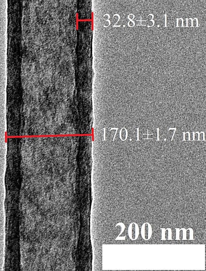
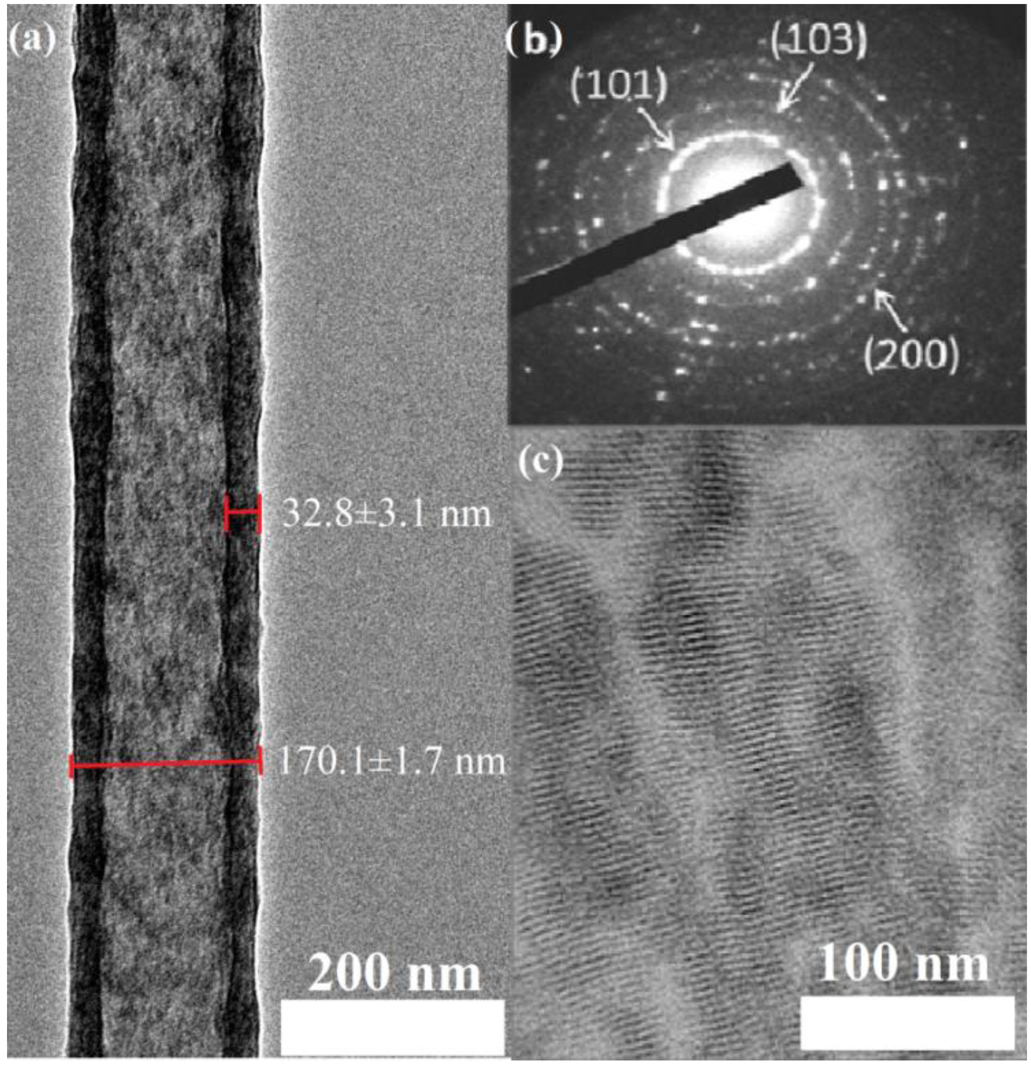
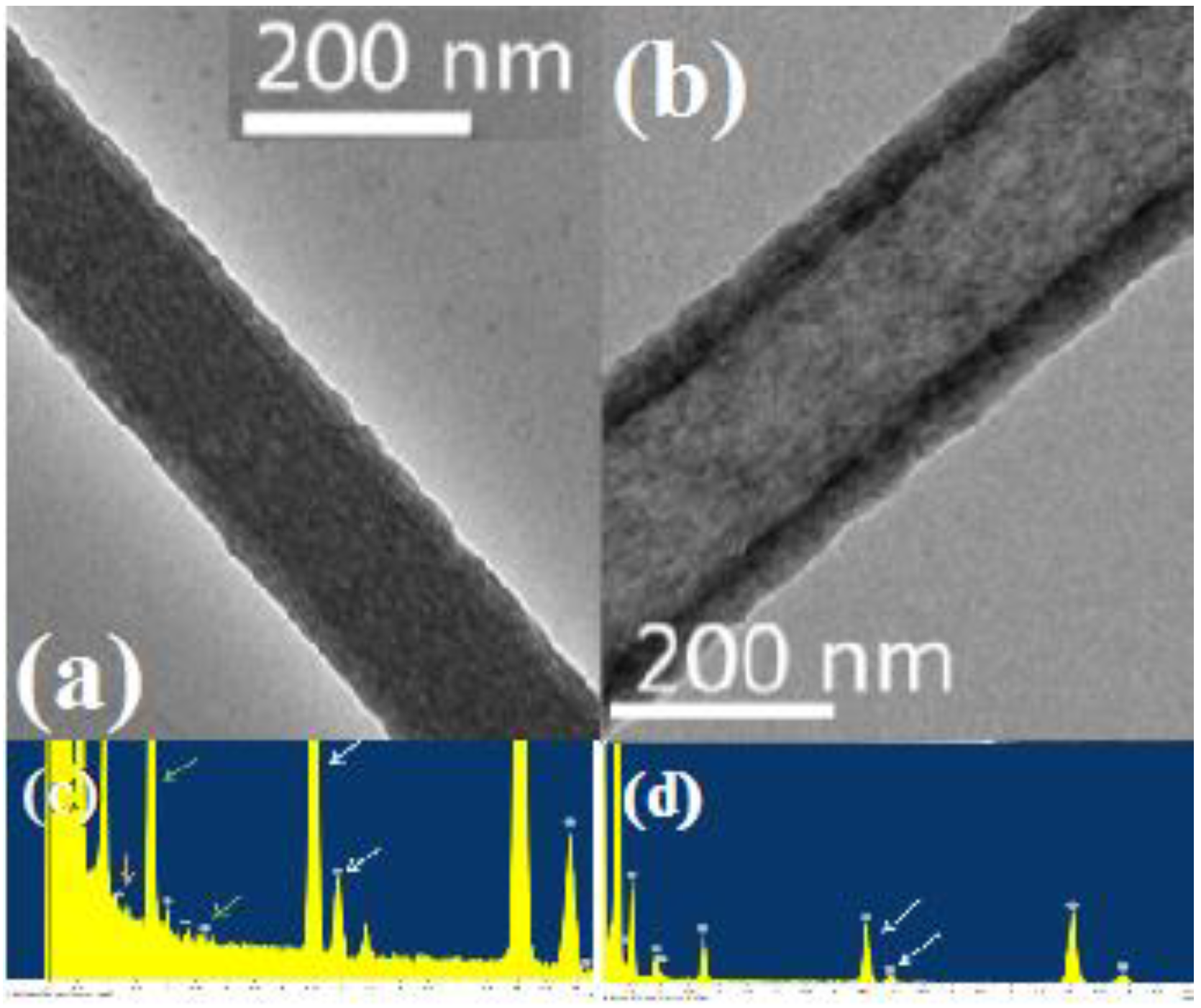
2.1. Characterization of Morphology and Material Composition

The TEM micrographs (Figure 1a and Figure 2a,b) show the individual TiO2 and PbSe/TiO2 nanotube morphology and overall nanocomposite arrangement. The uniformity and arrangement of the synthesized TiO2 nanotubes can be seen in Figure 1a. This shows that the nanotubes are of a very uniform outer diameter of 170.1 ± 1.7 nm, with a very uniform wall thickness of 32.8 ± 3.1 nm. These averages and standard deviations are taken from ten different electrospun samples, each with ten different fiber diameters and wall thicknesses measured. This relatively small wall thickness maximizes the surface area of which PbSe nanostructures can be loaded onto the inner wall of the TiO2 nanotubes and lowers the thickness of the TiO2, which helps to reduce electron-hole recombination as the hot electrons will be transported through the TiO2 to the electrodes. Figure 1b shows an electron diffraction pattern indicating that the TiO2 is in the anatase crystal phase. This polymorphic crystalline phase of TiO2 is a well-known type used in photocatalytic and photovoltaic applications due to its excellent charge-carrier extraction. Figure 1c shows the stand-alone PbSe nanostructures. These structures consist of angstrom-scale 0D lead selenide crystals, synthesized via a solvothermal route, which have stacked into 1D nanorods via aligned dipoles. These 1D nanorods have arranged into nanoscale 2D sheets via directional short-ranged attractions.
Figure 1. (a) TEM micrograph showing the high uniformity and reproducibility of the electrospun hollow TiO2 nanotube diameter and wall thickness, each with very small standard deviations; (b) Electron diffraction pattern indicating the presence of anatase TiO2; (c) TEM micrograph of the standalone PbSe nanostructures.
Fibers 03 00173 g001
Figure 2 shows the TiO2 nanotubes with and without the PbSe nanostructures deposited on the inner walls. It can be seen that the overall morphology of the nanocomposite is not changed upon implementation of the PbSe nanostructures. The wall thicknesses and fiber diameters remain within standard error regardless of the introduction of the nanostructures being co-electrospun within. The energy dispersive X-ray spectroscopy (EDX) analysis shown in Figure 2c (TiO2 loaded with PbSe) shows both major and minor peaks of: Titanium (Kα = 4.5 keV, Lα = 0.4 keV), Oxygen (Kα = 0.5 keV), Lead (Lα = 10.5 keV, Mα = 2.3 keV), and Selenium (Kα = 11.2 keV, Lα = 1.3 keV), showing the presence of both TiO2 and PbSe. The EDX analysis shown in Figure 2d (neat TiO2) shows both major and minor peaks of: Titanium, Oxygen, showing only the presence of TiO2. The relative ratios of these peaks all agrees with the presence of TiO2 and PbSe. The copper and carbon peaks are due to the TEM grid.
Figure 2. TEM micrographs of the TiO2 nanotubes (a) with and (b) without the PbSe nanostructures, illustrating that the PbSe nanostructures can be implemented into the TiO2 nanotubes without changing the overall nanocomposite morphology. EDX analysis of the TiO2 nanotubes (c) with and (d) without the PbSe nanostructures, showing (in (c)) an equal ratio of Pb and Se and the presence of the PbSe nanostructures.
Fibers 03 00173 g002

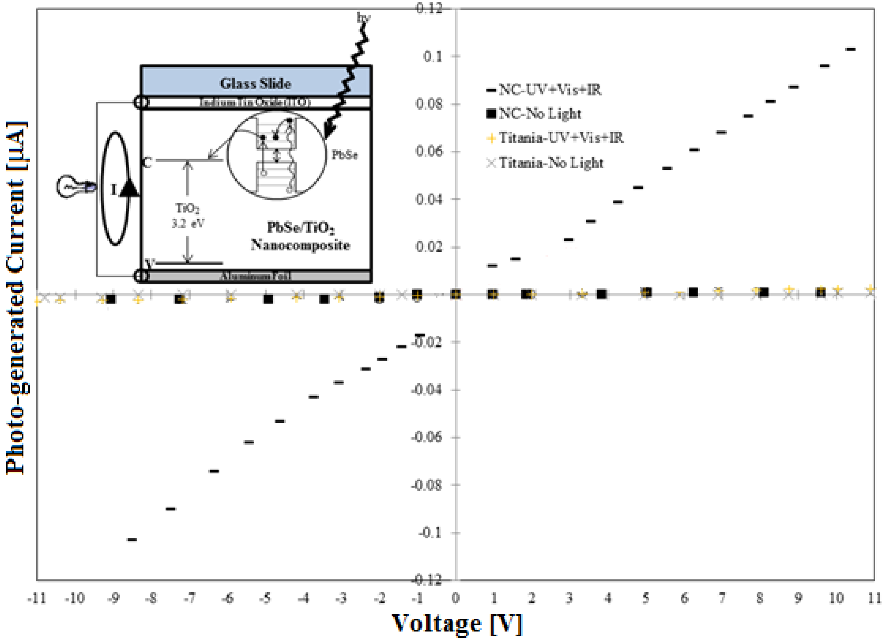
2.2. Photovoltaic Characterization

To demonstrate the photovoltaic nature of the synthesized PbSe/TiO2 nanocomposite, a device was fabricated as seen in the inset of Figure 3. This schematic shows the energy band diagram for the formation of multiple excitons in PbSe and the electron injection into TiO2. The flow of current through the fabricated testing device, an indium tin oxide (ITO)/nanocomposite/aluminum foil sandwich, is also shown in the Figure 3 inset.
The current-voltage curves in Figure 3 show that there is a clear difference between the dark-current (un-illuminated) and the photo-current (illuminated with UV-Vis-IR) testing of the nanocomposite. It is clear that the sample illuminated under UV, visible, and IR wavelengths generates the highest current and shows linear behavior, suggesting enhanced electronic stability. These nanocomposite IV curves are compared to the photo-generated current of the TiO2 electrospun nanotubes with the same configuration, only without the PbSe. These samples showed much lower photo-generated currents and illumination of any wavelength did not seem to show a significant difference from the dark-current curve. This shows that the synthesized nanocomposite is indeed photovoltaic, and a photo-generated current can be collected from it easily. This proof-of-concept work has shown that co-electrospinning can be used as an effective PbSe/TiO2 nanocomposite photovoltaic material synthesis. These synthesized PbSe/TiO2- nanocomposite have shown that photo-generated current extraction is easily obtained through a simple device and under further characterization and optimization this nanocomposite has the potential to have an increased quantum efficiency and efficient charge-carrier extraction. The high surface area, high interfacial connectivity, and tailorable nature make the developed nanocomposite an excellent energy-harvesting candidate for a scalable synthesis for both human and robotic extraterrestrial travel and colonization, as well as terrestrial travel and day-to-day modern life. Further experimentation will include use of different collectors for better alignment, exploration of other configuration, as well as tuning of the PbSe nanostructure diameters to optimize absorption.
Figure 3. Current-Voltage (IV) curves for dark-current and photo-current testing of the electrospun nanocomposite compared to the neat electrospun TiO2 (inset: Schematic showing the energy band diagram for the nanocomposite and the flow of current through the fabricated testing device. This consists of the test material—either the neat anatase titania or the nanocomposite—sandwiched between aluminum foil and an ITO-coated glass slide).
Fibers 03 00173 g003
The current-voltage curves in Figure 3 show that there is a clear difference between the dark-current (un-illuminated) and the photo-current (illuminated with UV-Vis-IR) testing of the nanocomposite. It is clear that the sample illuminated under UV, visible, and IR wavelengths generates the highest current and shows linear behavior, suggesting enhanced electronic stability. These nanocomposite IV curves are compared to the photo-generated current of the TiO2 electrospun nanotubes with the same configuration, only without the PbSe. These samples showed much lower photo-generated currents and illumination of any wavelength did not seem to show a significant difference from the dark-current curve. This shows that the synthesized nanocomposite is indeed photovoltaic, and a photo-generated current can be collected from it easily. This proof-of-concept work has shown that co-electrospinning can be used as an effective PbSe/TiO2 nanocomposite photovoltaic material synthesis. These synthesized PbSe/TiO2- nanocomposite have shown that photo-generated current extraction is easily obtained through a simple device and under further characterization and optimization this nanocomposite has the potential to have an increased quantum efficiency and efficient charge-carrier extraction. The high surface area, high interfacial connectivity, and tailorable nature make the developed nanocomposite an excellent energy-harvesting candidate for a scalable synthesis for both human and robotic extraterrestrial travel and colonization, as well as terrestrial travel and day-to-day modern life. Further experimentation will include use of different collectors for better alignment, exploration of other configuration, as well as tuning of the PbSe nanostructure diameters to optimize absorption.

3. Materials and Methods

3.1. Chemicals

Tri-n-octylphosphine (TOP), selenium powder, lead acetate trihydrate, oleic acid, n-tetradecylphosphonic acid, and diphenyl ether were purchased from Sigma-Aldrich (St. Louis, MO, USA) for the synthesis of the PbSe nanostructures. Titanium iso-propoxide (TIP), absolute ethanol, acetic acid (AA), and poly (vinyl pyrrolidone) (PVP) were purchased for electrospinning through Sigma-Aldrich.

3.2. PbSe Nanostructure Preparation

All syntheses were done under dry nitrogen. The synthesis of the PbSe nanostructures followed an existing synthesis route [48] with a few minor modifications. A 1.0 M stock solution of TOPSe was prepared by adding 7.86 g of selenium to 100 mL of TOP and mixing for 2 h at 50 °C. Lead oleate was formed in situ by mixing 0.76 g of lead acetate trihydrate with 2 mL of oleic acid in 10 mL diphenyl ether and heating for 30 min at 150 °C for 30 min under nitrogen flow via a bubbler. The lead oleate solution was then cooled to 60 °C and 4 mL of TOPSe is added to this solution. This solution is referred to as the lead oleate-TOPSe solution.
In a separate jar, 0.2 g of n-tetradecylphosphonic acid is added to 15 mL of diphenyl ether and this solution is heated to 250 °C with vigorous stirring. The lead oleate-TOPSe solution is added to the solution of n-tetradecylphosphonic acid in diphenyl ether. The final solution is heated for 50 s at 250 °C and then cooled to room temperature. While the solution cools down, the solution turns cloudy, indicating the formation of the PbSe nanostructures. Finally, 31 mL of hexane is added to this solution. The PbSe nanostructures can be centrifuged and re-suspended in different solvents such as chloroform, water, and THF. They are left in hexane for the purposes of electrospinning.

3.3. TiO2 Nanotube Preparation

The TiO2 electrospinning solution is made by mixing the following two solutions in a capped vial: (1) 3 mL of ethanol mixed with 3 mL acetic acid and 1.5 g TIP and (2) 7.5 mL ethanol and 0.45 g PVP. Once the two solutions are combined, cap and mix rigorously with magnetic stirrer for 1 h. If using again after allowing the solution to sit for a period of time, additional mixing or sonication is required.

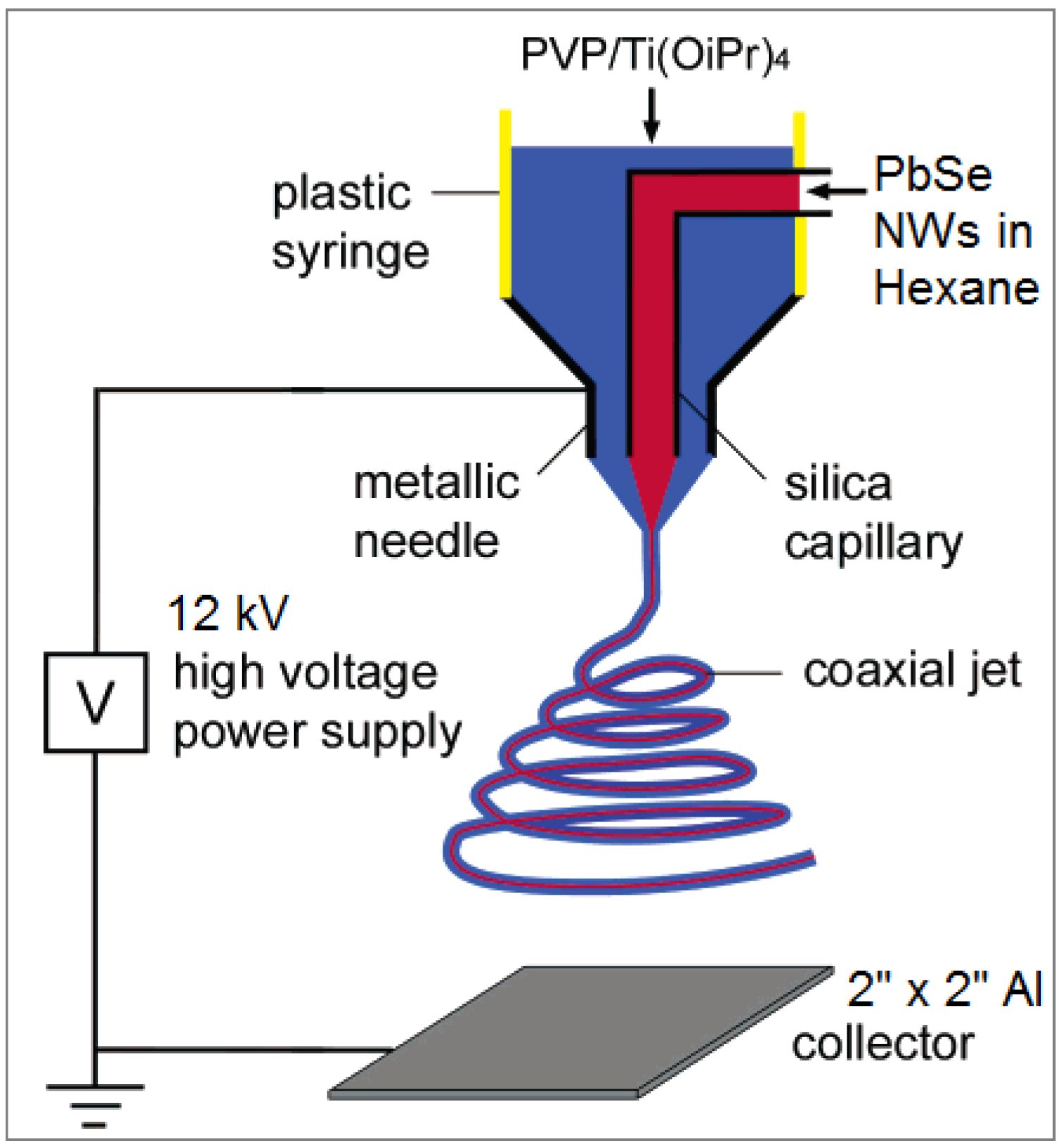
3.4. Electrospinning Setup and Conditions

The electrospinning setup, which can be seen in Figure 4, follows reference [29], with modifications to the working conditions. During typical procedures, a voltage of 12 kV was applied between the 9cm gap between the needle tip and the 2″ × 2″ aluminum foil collector. The PbSe solution was pumped at a rate of 0.6 mL/h and the TiO2 solution was pumped at a rate of 0.38 mL/h, both through Harvard Apparatus syringe infusion pump 22. Once complete, the nanotubes were left on the collector in air overnight to allow the TIP to hydrolyze and calcined at 400 °C for 30 min, then increased every thirty minutes by 50 °C, up to 550 °C, where it was held for 4.5 h. This morphed the amorphous TiO2 to anatase crystallinity. Once calcined, the samples were ready for characterization.
Figure 4. A schematic illustration of the co-axial spinneret, adapted with permission from [29]. Copyright 2004 American Chemical Society.
Fibers 03 00173 g004

3.5 Characterization

Transmission electron microscopy (TEM) and energy dispersive X-ray spectroscopy (EDX) of the PbSe/TiO2 nanocomposite was done on a JEOL JEM 2100 instrument (JEOL USA, Inc., Peabody, MA, USA) operated at 200 keV using copper 100/200 square mesh grids (Electron Microscopy Sciences). Electronic characterization, adapted from references [39,49], of the photovoltaic nanocomposite were performed on a fabricated device, as shown in Figure 3 inset, and data was collected using a digital multimeter and a Vernier LabPro data collection device connected to a PC.

Acknowledgments

This work has been supported in part by the NASA funded Rhode Island Space Grant Consortium, the University of Rhode Island Transportation Center grant, and the Honda Initiation Grant. The authors would also like to thank Santosha Ammu for her photovoltaic characterization contributions.

Author Contributions

Evan K. Wujcik and Stephanie R. Aceto provided all experimental results, while David Heskett provided interpretations and analysis of the results. Evan K. Wujcik and Arijit Bose oversaw the writing and preparation of the manuscript.

Conflicts of Interest

The authors declare no conflict of interest.

References

  1. Maniyali, Y.; Almansoori, A.; Fowler, M.; Elkamel, A. Energy hub based on nuclear energy and hydrogen energy storage. Ind. Eng. Chem. Res. 2013, 52, 7470–7481. [Google Scholar] [CrossRef]
  2. Thavasi, V.; Singh, G.; Ramakrishna, S. Electrospun nanofibers in energy and environmental applications. Energ. Environ. Sci. 2008, 1, 205–221. [Google Scholar] [CrossRef]
  3. ASTM International. ASTM G173-03(2012). Standard Tables for Reference Solar Spectral Irradiances: Direct Normal and Hemispherical on 37° Tilted Surface; ASTM International: West Conshohocken, PA, USA, 2012. [Google Scholar]
  4. Pohekar, S.D.; Kumar, D.; Ramachandran, M. Dissemination of cooking energy alternatives in India—A review. Renew. Sustain. Energ. Rev. 2005, 9, 379–393. [Google Scholar] [CrossRef]
  5. Nault, R.M. Basic Research Needs for Solar Energy Utilization; United States Department of Energy: Washington, DC, USA, 2005.
  6. EL-Shimy, M. Viability analysis of PV power plants in Egypt. Renew. Energ. 2009, 34, 2187–2196. [Google Scholar] [CrossRef]
  7. Mankins, J.C. New directions for space solar power. Acta Astronaut. 2009, 65, 146–156. [Google Scholar] [CrossRef]
  8. Chen, J.-Y.; Wu, H.-C.; Chiu, Y.-C.; Chen, W.-C. Plasmon-enhanced polymer photovoltaic device performance using different patterned Ag/PVP electrospun nanofibers. Adv. Energ. Mater. 2014, 4. [Google Scholar] [CrossRef]
  9. Börjesson, K.; Lennartson, A.; Moth-Poulsen, K. Efficiency limit of molecular solar thermal energy collecting devices. ACS Sustain. Chem. Eng. 2013, 1, 585–590. [Google Scholar] [CrossRef]
  10. Kim, J.-U.; Park, S.-H.; Choi, H.-J.; Lee, W.-K.; Lee, J.-K.; Kim, M.-R. Effect of electrolyte in electrospun poly (vinylidene fluoride-co-hexafluoropropylene) nanofibers on dye-sensitized solar cells. Solar Energ. Mater. Solar Cell. 2009, 93, 803–807. [Google Scholar] [CrossRef]
  11. Park, J.-Y.; Lee, J.-W.; Park, K.H.; Kim, T.-Y.; Yim, S.-H.; Zhao, X.G.; Gu, H.-B.; Jin, E.M. Dye-sensitized solar cells based on electrospun poly (vinylidenefluoride-co-hexafluoropropylene) nanofibers. Polym. Bull. 2013, 70, 507–515. [Google Scholar] [CrossRef]
  12. Grätzel, M. Solar Energy conversion by dye-sensitized photovoltaic cells. Inorg. Chem. 2005, 44, 6841–6851. [Google Scholar] [CrossRef] [PubMed]
  13. O’Regan, B.; Grätzel, M. A low-cost, high-efficiency solar cell based on dye-sensitized colloidal TiO2 films. Nature 1991, 353, 737–740. [Google Scholar] [CrossRef]
  14. Kim, B.-G.; Park, H.J. Novel conjugated polymer for organic photovoltaics: Synthesis and device optimization. Synth. Met. 2015, 199, 280–283. [Google Scholar] [CrossRef]
  15. Pathak, D.; Wagner, T.; Adhikari, T.; Nunzi, J.M. Photovoltaic performance of AgInSe2-conjugated polymer hybrid system bulk heterojunction solar cells. Synth. Met. 2015, 199, 87–92. [Google Scholar] [CrossRef]
  16. Peumans, P.; Uchida, S.; Forrest, S.R. Efficient bulk heterojunction photovoltaic cells using small-molecular-weight organic thin films. Nature 2003, 425, 158–162. [Google Scholar] [CrossRef] [PubMed]
  17. Tang, Z.; Liu, B.; Melianas, A.; Bergqvist, J.; Tress, W.; Bao, Q.; Qian, D.; Inganäs, O.; Zhang, F. A new fullerene-free bulk-heterojunction system for efficient high-voltage and high-fill factor solution-processed organic photovoltaics. Adv. Mater. 2015, 27, 1900–1907. [Google Scholar] [CrossRef] [PubMed]
  18. Kamat, P.V. Quantum dot solar cells. Semiconductor nanocrystals as light harvesters. J. Phys. Chem. C 2008, 112, 18737–18753. [Google Scholar] [CrossRef]
  19. Yang, S.; Nair, S.; Ramakrishna, S. Morphology of the electrospun TiO2 on the photovoltaic properties of CdS quantum dot-sensitized solar cells. J. Nanosci. Nanotechnol. 2015, 15, 721–725. [Google Scholar]
  20. Nozik, A.J. Quantum dot solar cells. Phys. E Low dimens. Syst. Nanostruct. 2002, 14, 115–120. [Google Scholar] [CrossRef]
  21. Schaller, R.D.; Sykora, M.; Pietryga, J.M.; Klimov, V.I. Seven excitons at a cost of one: Redefining the limits for conversion efficiency of photons into charge carriers. Nano Lett. 2006, 6, 424–429. [Google Scholar] [CrossRef] [PubMed]
  22. Liu, J.; Huang, J.; Wujcik, E.K.; Qiu, B.; Rutman, D.; Zhang, X.; Salazard, E.; Wei, S.; Guo, Z. Hydrophobic Electrospun Polyimide Nanofibers for Self-cleaning Materials. Macromol. Mate. Eng. 2015, 300, 358–368. [Google Scholar] [CrossRef]
  23. Wujcik, E.K. Synthesis of Lead Selenide-titania Heterostructures for High-efficiency Low-cost Solar Cells. Master’s Thesis, The University of Rhode Island, Kingston, RI, USA, 2009. [Google Scholar]
  24. Valiquette, D.; Pellerin, C. Miscible and core-sheath PS/PVME fibers by electrospinning. Macromolecules 2011, 44, 2838–2843. [Google Scholar] [CrossRef]
  25. Wujcik, E.K. Discovery of Nanostructured Material Properties for Advanced Sensing Platforms. Electronic Dissertation, The University of Akron, Akron, OH, USA, 2013. [Google Scholar]
  26. Sharma, J.; Lizu, M.; Stewart, M.; Zygula, K.; Lu, Y.; Chauhan, R.; Yan, X.; Guo, Z.; Wujcik, E.K.; Wei, S. Multifunctional Nanofibers towards active biomedical therapeutics. Polymers 2015, 7, 186–219. [Google Scholar] [CrossRef]
  27. Chen, M.; Qu, H.; Zhu, J.; Luo, Z.; Khasanov, A.; Kucknoor, A.S.; Haldolaarachchige, N.; Young, D.P.; Wei, S.; Guo, Z. Magnetic electrospun fluorescent polyvinylpyrrolidone nanocomposite fibers. Polymer 2012, 53, 4501–4511. [Google Scholar] [CrossRef]
  28. Peng, Q.; Sun, X.-Y.; Spagnola, J.C.; Hyde, G.K.; Spontak, R.J.; Parsons, G.N. Atomic layer deposition on electrospun polymer fibers as a direct route to Al2O3 microtubes with precise wall thickness control. Nano Lett. 2007, 7, 719–722. [Google Scholar] [CrossRef] [PubMed]
  29. Li, D.; Xia, Y. Direct fabrication of composite and ceramic hollow nanofibers by electrospinning. Nano Lett. 2004, 4, 933–938. [Google Scholar] [CrossRef]
  30. Li, D.; Wang, Y.; Xia, Y. Electrospinning of polymeric and ceramic nanofibers as uniaxially aligned arrays. Nano Lett. 2003, 3, 1167–1171. [Google Scholar] [CrossRef]
  31. Blasdel, N.J.; Wujcik, E.K.; Carletta, J.E.; Lee, K.-S.; Monty, C.N. Fabric nanocomposite resistance temperature detector. IEEE Sens. J. 2015, 15, 300–306. [Google Scholar] [CrossRef]
  32. Monty, C.; Wujcik, E.K.; Blasdel, N. Flexible Electrode for Detecting Changes in Temperature, Humidity, and Sodium Ion Concentration in Sweat. US 20130197319 A1, 1 August 2013. [Google Scholar]
  33. Wujcik, E.K.; Blasdel, N.J.; Trowbridge, D.; Monty, C.N. Ion sensor for the quantification of sodium in sweat samples. IEEE Sens. J. 2013, 13, 3430–3436. [Google Scholar] [CrossRef]
  34. Wang, H.; Oey, C.C.; Djurišić, A.B.; Xie, M.H.; Leung, Y.H.; Man, K.K.Y.; Chan, W.K.; Pandey, A.; Nunzi, J.-M.; Chui, P.C. Titania bicontinuous network structures for solar cell applications. Appl. Phys. Lett. 2005, 87. [Google Scholar] [CrossRef]
  35. Shankar, K.; Paulose, M.; Mor, G.K.; Varghese, O.K.; Grimes, C.A. A study on the spectral photoresponse and photoelectrochemical properties of flame-annealed titania nanotube-arrays. J. Phys. D Appl. Phys. 2005, 38, 3543–3549. [Google Scholar] [CrossRef]
  36. Du, A.; Ng, Y.H.; Bell, N.J.; Zhu, Z.; Amal, R.; Smith, S.C. Hybrid graphene/titania nanocomposite: Interface charge transfer, hole doping, and sensitization for visible light response. J. Phys. Chem. Lett. 2011, 2, 894–899. [Google Scholar] [CrossRef]
  37. Silipas, T.D.; Indrea, E.; Dreve, S.; Suciu, R.-C.; Rosu, M.C.; Danciu, V.; Cosoveanu, V.; Popescu, V. TiO2––Based systems for photoelectrochemical generation of solar hydrogen. J. Phys. Conf. Ser. 2009, 182. [Google Scholar] [CrossRef]
  38. Masuda, Y.; Ohji, T.; Kato, K. Multineedle TiO2 nanostructures, self-assembled surface coatings, and their novel properties. Cryst. Growth Des. 2010, 10, 913–922. [Google Scholar] [CrossRef]
  39. Kim, S.J.; Kim, W.J.; Sahoo, Y.; Cartwright, A.N.; Prasad, P.N. Multiple exciton generation and electrical extraction from a PbSe quantum dot photoconductor. Appl. Phys. Lett. 2008, 92. [Google Scholar] [CrossRef]
  40. Schaller, R.; Klimov, V. High efficiency carrier multiplication in pbse nanocrystals: Implications for solar energy conversion. Phys. Rev. Lett. 2004, 92. [Google Scholar] [CrossRef]
  41. Ellingson, R.J.; Beard, M.C.; Johnson, J.C.; Yu, P.; Micic, O.I.; Nozik, A.J.; Shabaev, A.; Efros, A.L. Highly efficient multiple exciton generation in colloidal PbSe and PbS Quantum dots. Nano Lett. 2005, 5, 865–871. [Google Scholar] [CrossRef] [PubMed]
  42. Beard, M.C.; Midgett, A.G.; Law, M.; Semonin, O.E.; Ellingson, R.J.; Nozik, A.J. Variations in the Quantum efficiency of multiple exciton generation for a series of chemically treated PbSe nanocrystal films. Nano Lett. 2009, 9, 836–845. [Google Scholar] [CrossRef] [PubMed]
  43. Luther, J.M.; Beard, M.C.; Song, Q.; Law, M.; Ellingson, R.J.; Nozik, A.J. Multiple exciton generation in films of electronically coupled PbSe quantum dots. Nano Lett. 2007, 7, 1779–1784. [Google Scholar] [CrossRef] [PubMed]
  44. Allan, G.; Delerue, C. Role of impact ionization in multiple exciton generation in PbSe nanocrystals. Phys. Rev. B 2006, 73, 205423. [Google Scholar] [CrossRef]
  45. Alcoutlabi, M.; McKenna, G.B. Effects of confinement on material behaviour at the nanometre size scale. J. Phys. Condens. Matter 2005, 17, R461–R524. [Google Scholar] [CrossRef]
  46. Kamperman, M.; Korley, L.T.J.; Yau, B.; Johansen, K.M.; Joo, Y.L.; Wiesner, U. Nanomanufacturing of continuous composite nanofibers with confinement-induced morphologies. Polym. Chem. 2010, 1, 1001–1004. [Google Scholar] [CrossRef]
  47. Yu, W.W.; Falkner, J.C.; Shih, B.S.; Colvin, V.L. Preparation and characterization of monodisperse PbSe semiconductor nanocrystals in a noncoordinating solvent. Chem. Mater. 2004, 16, 3318–3322. [Google Scholar]
  48. Cho, K.-S.; Talapin, D.V.; Gaschler, W.; Murray, C.B. Designing PbSe nanowires and nanorings through oriented attachment of nanoparticles. J. Am. Chem. Soc. 2005, 127, 7140–7147. [Google Scholar] [CrossRef] [PubMed]
  49. Yong, K.-T.; Sahoo, Y.; Choudhury, K.R.; Swihart, M.T.; Minter, J.R.; Prasad, P.N. Shape control of PbSe nanocrystals using noble metal seed particles. Nano Lett. 2006, 6, 709–714. [Google Scholar]

