1. Introduction
Electron beam and vacuum arc evaporation are widely used for deposition of thin films on various products at the gas pressure ranging from 0.01 to 1 Pa. The arc evaporation [
1,
2] is remarkable for a high deposition rate, and a high enough plasma density near the product surface. This ensures an adequate current of ions bombarding the negatively biased products. For example, this enables modification of the surface properties and structure of the cutting tools made of high-speed steel and other industrial products [
3].
The metal droplets arriving at the thin films from the arc cathode spots and nonuniformity of the discharge plasma in the process chamber are the main drawbacks of the vacuum arc. For the deposition of thin films, not containing the droplets, the filtered vacuum arc plasma [
4] can be used.
Another well-established technique for the thin film deposition is magnetron sputtering [
5,
6]. It allows the deposition of high-quality films without droplets. Regrettably, the target of a planar magnetron is sputtered only under the arc-shaped magnetic field on its surface. For this reason, the use efficiency of the target material is very low. It was shown in [
7,
8] that the material is used more efficiently when the target is placed at the bottom of a hollow cathode.
The film properties depend on the energy of condensing atoms. When this energy is transported to the film surface by accelerated ions, ion-assisted film deposition takes place [
9]. In this case, the energy supplied to the condensing film atoms is independent of the substrate temperature. It enables the film deposition on substrates made of heat-sensitive materials.
The ion bombardment improves film adhesion. The latter grows monotonically with the ion energy, due to deeper penetration of accelerated particles into the film [
10]. However, the increase in the ion energy results in sputtering of the growing film. When the ion energy rises to 1–3 keV, all deposited atoms can be sputtered [
11]. This means that for modification of the growing films by high-energy ions, the pulsed bombardment should be used. For instance, the pulsed bombardment by 45 keV ions of a titanium nitride film growing on a substrate made of high-speed steel resulted in the production of nc-Ti
2N/nc-TiN nanocomposite with microhardness up to 5000 HV0.04 [
12,
13,
14]. Due to mixing by high-energy particles of the film atoms and substrate atoms, the interface width increases up to 1 μm. It ensures a perfect adhesion of titanium nitride coatings with a thickness up to 50 μm. On a smaller scale, the same trends are characteristic of thin films deposited with film thicknesses ranging from 50 to 1000 nm [
11].
In order to bombard films growing on electrically conducting substrates with energetic ions, it is necessary to apply a negative voltage to the substrate. Hence, ions will be accelerated from the gas discharge. However, the plasma density near the substrate might be relatively low when magnetron sputtering is used. Only with the use of unbalanced magnetrons [
15] the plasma density grows to a value ensuring a sufficient current density of ions bombarding the substrate surface.
It is impossible to apply a negative potential to the surface of dielectric substrates. However, a dielectric substrate immersed in a plasma can also be bombarded by energetic ions accelerated from the plasma. The only requirement is to place the substrate on a conductive holder connected to a RF power supply. The negative potential of the substrate surface induced, in this case, can reach hundreds of volts [
16]. This allows sputtering of the dielectric surface by argon ions. Still, this technique cannot be used for uniform etching of complex-shaped dielectric substrates, for example, substrates with deep cavities. In this case, properties of the films on dielectric substrates can be regulated only with the use of broad beam sources of ions [
17,
18] or fast neutral atoms [
19,
20,
21,
22].
Only a small part of the target material is deposited on the substrates when planar magnetron sputtering is used, and the rest is lost on the chamber walls. Deposition of thin films made of gold or other precious metals requires minimizing of the target material losses. A sputtering system was developed on the base of the hollow cathode glow discharge to solve this problem [
11]. The central part of the system is a stainless steel hollow cathode 260 mm diameter and 100 mm deep, and covered with a 200 mm diameter grid. An electrostatic trap for electrons of the discharge plasma is formed [
23] when the grid is negative to the cathode. Multiplication of the fast electrons in the cathode sheath of the discharge [
24] allows maintaining the glow discharge without the magnetic field at the pressure of 0.1–1 Pa. This pressure range is also characteristic of the magnetron discharge.
The inner walls of the hollow cathode are covered with copper foils, and the grid is produced of the same foil. Copper was chosen for modeling the deposition of precious metals because its adhesion to glass and coefficient of sputtering by argon ions are close to the corresponding values for gold. Sputtering of the foil by ions from the discharge plasma results in a quite homogeneous distribution of the sputtered atom density inside the cathode. Through the grid orifices, the metal atoms enter the process vacuum chamber together with ions accelerated in the sheath between the plasma and the grid. Due to charge exchange collisions [
25], the ions turn into fast neutral atoms, which bombard the film growing on the substrate. Kinetic energy
E of the fast atoms is regulated through variation of the grid potential.
It was shown in [
11] that the thin film adhesion really increased with the fast atom energy. However, the ratio of the flow of metal atoms, M, to the flow of fast atoms, A, arriving at the substrate was practically constant. With the increase in the fast atom energy,
E, they begin to sputter the growing film, and at
E > 600 eV all deposited atoms are resputtered. The present research aims to solve the problem using a substantial increase in the ratio M/A, and pulsed bombardment of the growing coating. A new source of metal atoms and fast gas atoms was developed, with the sizes of its hollow cathode being equal to those of the cathode described in [
11] to achieve this aim.
2. Experimental and Methods
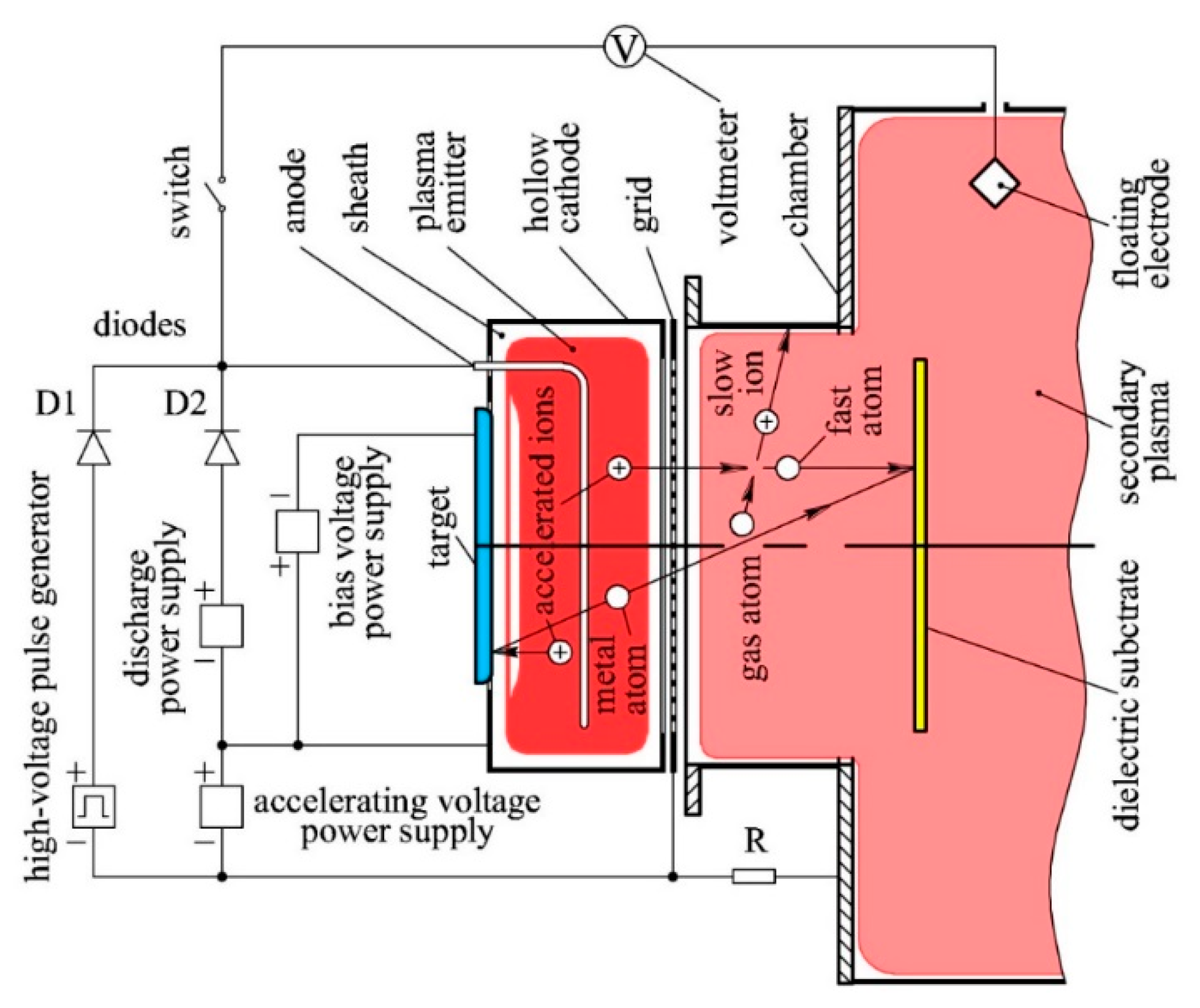
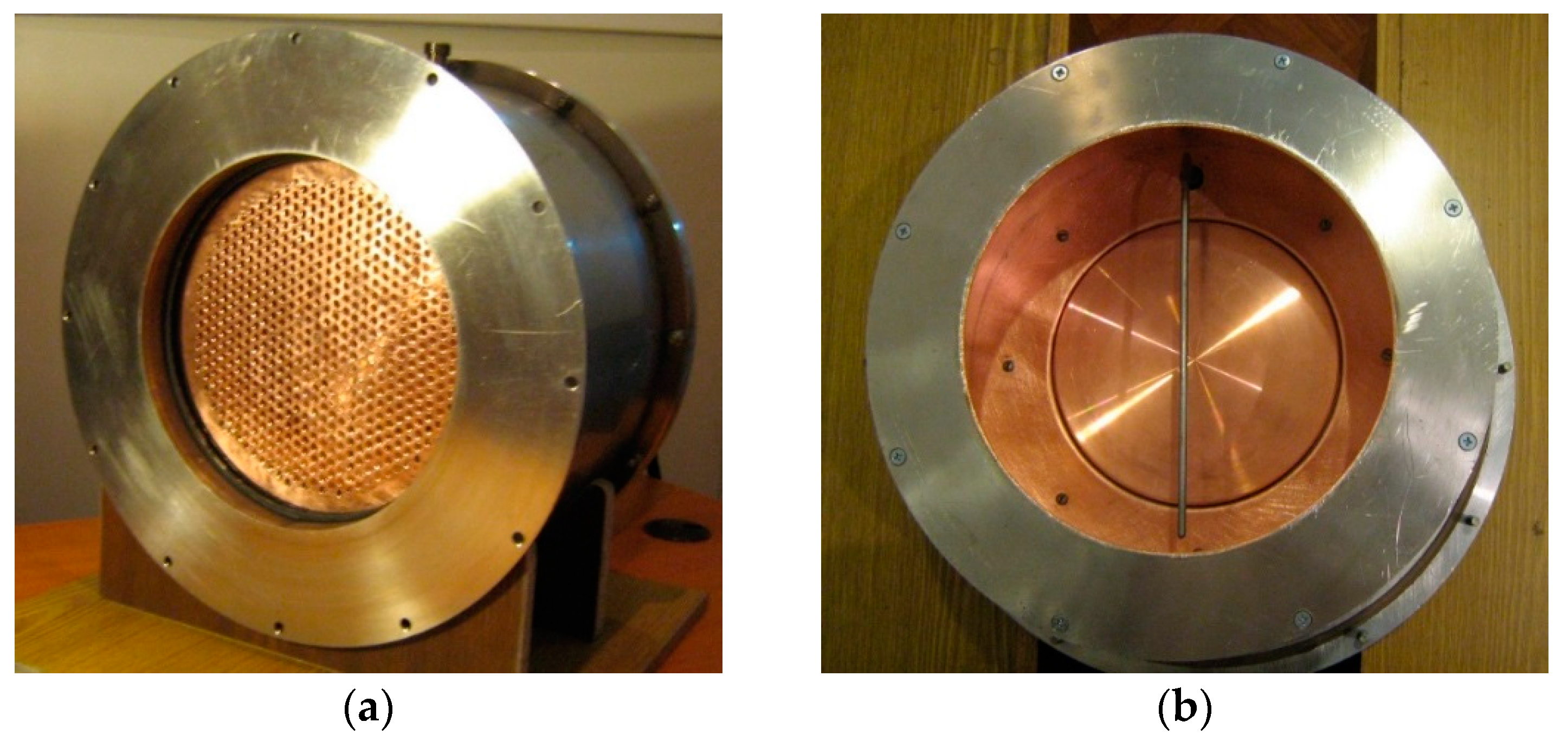
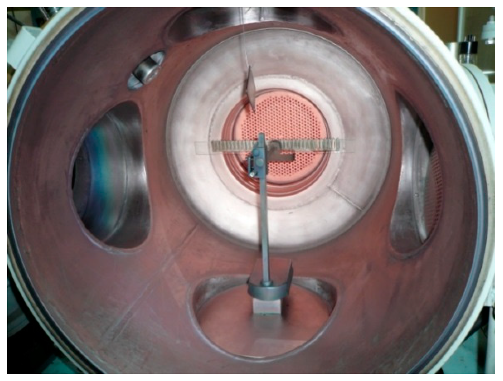
Figure 1 presents a schematic of the new source with a dismountable 260 mm diameter and 100 mm deep hollow cathode made of stainless steel. At the bottom of the hollow cathode, is placed a flat 160 mm diameter copper target cooled with water. The opposite 200 mm diameter aperture of the cathode is covered by a grid made of 0.7 mm-thick copper foil with 7 mm diameter or 5 mm diameter apertures (
Figure 2a). The centers of the apertures are distanced from each other at 8 mm.
The inner walls of the hollow cathode are covered with the same foil. An L-shaped anode made of a 5 mm diameter molybdenum rod (
Figure 2b) is introduced into the hollow cathode. A 200 mm-long vertical part of the anode is equally distant at 50 mm from the target and the grid. It was experimentally found that this shape of the anode facilitates the discharge ignition. The anode is coated with copper, and can be heated to a high temperature during the source operation.
The source is mounted on a 500 mm diameter and 600 mm-long grounded vacuum chamber pumped by a turbo-molecular pump and a rotary pump through a flat grounded grid (not shown in
Figure 1) to a base pressure of 0.001 Pa. The grid prevents the plasma filling the chamber from penetrating into the pumping system.
The source is equipped with three DC power supplies and one high-voltage pulse generator. The negative pole of the pulse generator is connected to the grid, and its positive pole through a diode D1 is connected to the anode. The device generates pulses with the amplitude regulated from 2 to 10 kV, at a width of 10 to 50 μs, and repetition rate ranging from 10 to 50 Hz. The negative pole of the discharge power supply is connected to the hollow cathode, and its positive pole through a high-voltage diode D2 connected to the anode. It allows a stabilized discharge current in the anode circuit up to Id = 2 A at the discharge voltage Ud between the anode and the hollow cathode, up to 600 V. The bias voltage power supply is connected between the cathode and the target. It allows a stabilized voltage Ut between the hollow cathode and the target, up to 2 kV, at the current in the target circuit of up to It = 1 A. The grid is connected to the chamber through a resistor, R, with the resistance of 10 kΩ. The accelerating voltage power supply is connected between the hollow cathode and the grid. It allows a stabilized voltage Ua variable from 0.2 to 2 kV at the sum of the currents in the circuits of the grid and the chamber up to 1 A. The diode D1 prevents from the short-circuit of the discharge power supply and accelerating voltage power supply through the output transformer winding of the pulse generator. The high-voltage diode D2 prevents DC power supply damage from high-voltage pulses.
A gas pre-ionization system (not shown in
Figure 1) is mounted on the chamber wall. The gas supplied to the chamber through this system is weakly ionized; it is admitted from the chamber to the hollow cathode through the emissive grid of the source. As a result, the chamber and the hollow cathode are filled with low-density plasma. When the discharge power supply and the accelerating voltage power supply are switched on, the weakly ionized gas inside the hollow cathode initiates ignition of the glow discharge. As a result, the cathode is filled with homogeneous discharge plasma. The hollow cathode discharge operation is described, in detail, in [
23]. The plasma density inside the hollow cathode amounts to ~10
16 m
−3, and the temperature of the plasma electrons is close to 1 eV at the discharge current of 1 A. The accelerating voltage power supply always ensures the potential difference between the hollow cathode and the grid of at least 200 V. This prevents the electrons emitted by the cathode from leaving the hollow cathode through apertures of the grid [
22].
The plasma emitter is separated from the cathode and the grid surfaces by a sheath of positive space charge. The argon ions accelerated in the sheath between the plasma emitter and the grid enter the chamber through the grid apertures. The ions turn into fast atoms, which bombard a dielectric substrate placed in the chamber, because of the charge-exchange collisions with gas atoms. The secondary electrons, emitted by the chamber and the grid, neutralize the positive space charge of slow ions produced in the charge-exchange collisions. Secondary plasma is produced in the chamber in this way. The density of the secondary plasma is maximal near the grid, where most of the charge exchange collisions take place, and it monotonically decreases towards the opposite side of the chamber. The current of slow ions arriving at the chamber walls induces a potential drop of several hundred volts across the resistor, R, with the resistance of 10 kΩ. The negative potential of the grid, induced in this way, prevents electrons of the secondary plasma from penetration into the hollow cathode.
A floating electrode is immersed in the secondary plasma and the potential difference between them amounts to about 10 V. As the potential difference between the plasma emitter and the anode amounts to about the same value, the energy of ions accelerated between the secondary plasma and the plasma emitter corresponds to the voltage between the anode and the floating electrode. In these conditions, the energy of the fast atoms is equal to the energy of ions, and can be measured with a voltmeter.
A long 30 mm-wide glass substrate is positioned inside the chamber on a holder isolated from the chamber to study the spatial distribution of the film deposition rate (
Figure 3). The substrate is parallel to the grid, and crosses the source axis. Tens of masks are fastened on the substrate surface facing the grid.
The height of the steps between the masked and open surfaces of the substrate is measured using a stylus profiler DektakXT (produced by Bruker Nano Inc., Tucson, AZ, USA) after the film is deposited and the masks are detached from the substrate surface. Division of the step height by the deposition time yields the deposition rate. The argon ions are accelerated from the plasma emitter to the target surface and to the copper foil, which covers the inner surface of the hollow cathode. As a result, a copper vapor is produced inside the cathode. When the bias power supply is switched off, the energy of ions sputtering the target is equal to the energy of ions sputtering the foil. In this case, the spatial distribution of the copper atom density is the same as in [
11]. Applying an accelerating voltage exceeding 1 kV between the hollow cathode and the grid results in sputtering of all copper atoms deposited on the dielectric substrate. Thus, only structural defects are produced on the substrate surface by the fast argon atoms. The defects improve the film adhesion because they are condensation centers for the film to be grown.
The target is sputtered with a much higher intensity when a voltage of 2 kV is applied between the hollow cathode and the target. Thus, most of the copper atoms from the target surface arrive at the grid. They enter the chamber and deposit on the dielectric substrate surface through the grid apertures. Argon atoms bombard the growing copper film during the deposition. Their energy is variable, from 0.2 to 2 keV, and can be measured with a voltmeter (
Figure 1). When the voltmeter is disconnected from the anode, and the pulse generator is switched on, the pulsed beams of argon atoms, with energy up to 10 keV and a repetition rate of 50 Hz, are produced.
The film adhesion is measured using an adhesion tester PosiTest AT-M Manual produced by DeFelsko Corporation (Ogdensburg, NY, USA). Films for these measurements are deposited on 48 × 60 mm2 glass substrates. The substrate is positioned parallel to the grid at various distances from it. A mask is fastened on the substrate surface for measurement of the deposited film thickness. The height of the step between the masked and open surfaces of the substrate is measured after film deposition.
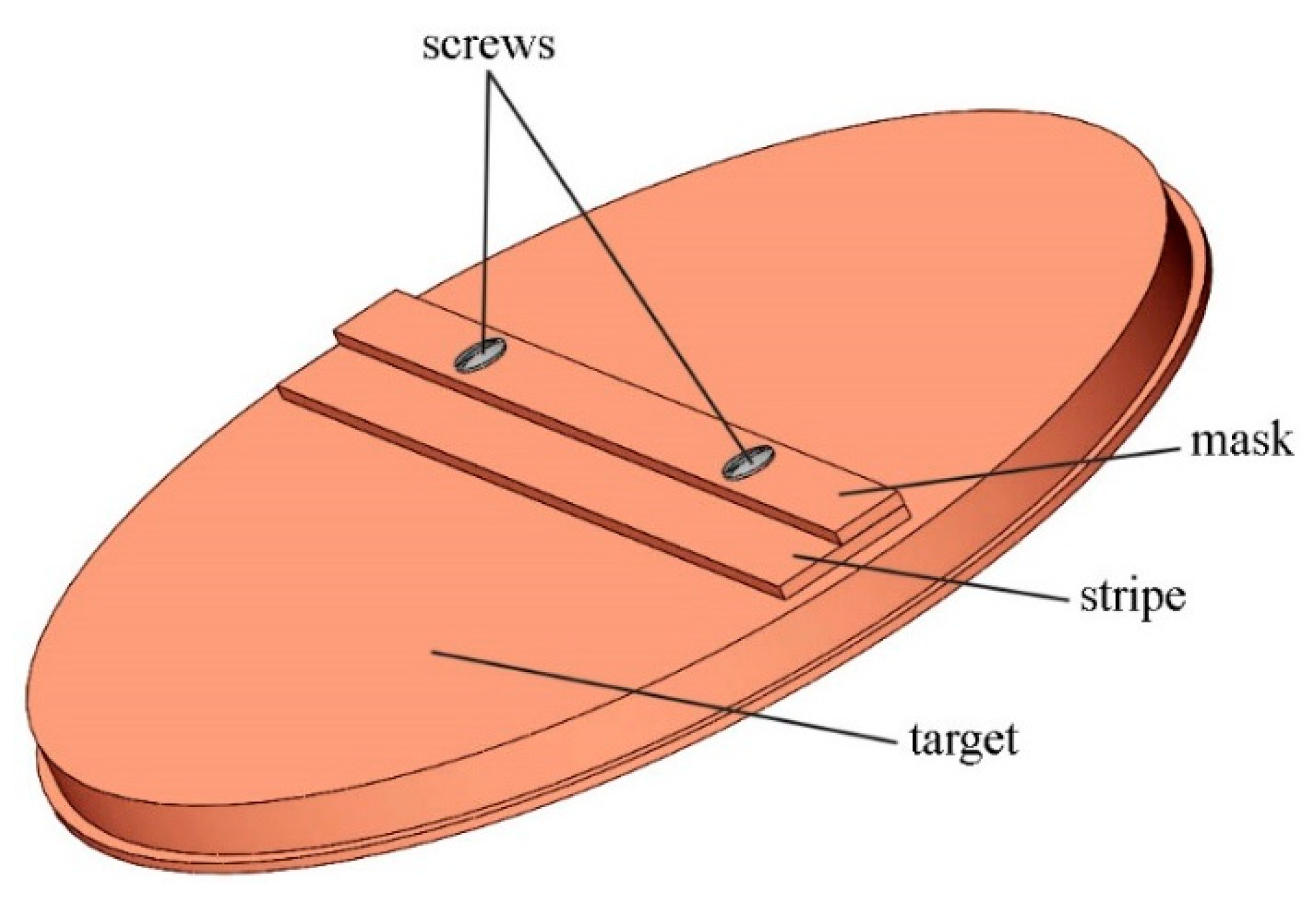
A 2 mm-thick, 20 mm-wide and 150 mm-long copper stripe is fastened on the target to obtain the distribution of the target sputtering rate (
Figure 4). The half of the stripe surface is covered with a 10 mm-wide and 150 mm-long copper mask. The line dividing the mask surface and the stripe surface passes through the target center. After the target sputtering, the stripe is detached from the target and the mask. The height of the steps between the masked and open surfaces of the stripe is measured at various distances from the stripe center using the stylus profiler DektakXT. Division of the step height by the etching time yields the etching rate.
3. Results
The discharge voltage between the anode and the cathode amounts to Ud = 400 V at the argon pressure p = 0.4 Pa, the discharge current in the anode circuit Id = 1.8 A, and voltage between the cathode and the grid of 200 V. In this case, the current in the chamber circuit amounts to Ich = 0.05 A, and current in the grid circuit amounts to Ig = 0.25 A. The potential difference measured with the voltmeter between the plasma emitter and the secondary plasma, which accelerates the ions, is equal to 100 V. The equivalent current of the 100 eV argon atoms, produced in the secondary plasma, amounts to Ib = η × (Ig + Ich) = 0.7 × (0.25 A + 0.05 A) = 0.21 A, where η = 0.7 is transparency of the grid with 7 mm diameter apertures. The potential difference between the grid and the chamber amounts to R × Ich = 10,000 Ω × 0.05 A = 500 V. It is adequate to prevent electrons of the secondary plasma from entering the hollow cathode through apertures of the grid. The increase in the accelerating voltage between the cathode and the grid up to 2 kV enables pretreatment of the dielectric substrate by neutral argon atoms with the energy of ~2 keV.
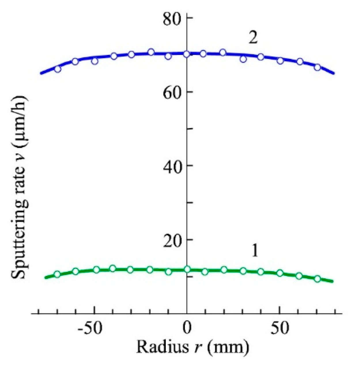
Curve 1 in
Figure 5 presents the radial distribution of the target sputtering rate at zero voltage between the hollow cathode and the target, the argon pressure
p = 0.4 Pa, and the discharge current in the anode circuit
Id = 1.8 A. It exhibits uniform sputtering of the 160 mm-diameter target by 400 eV argon ions.
It should be noted that sputtering of the inner cathode surface is not uniform. After a long operation, thick deposits of the target material are observed on the foils detached from the walls of the dismountable hollow cathode. The thickness of the deposits is maximal in the corners between the cylindrical and flat parts of the cathode surface, where the current density of the sputtering ions is minimal. The ion current density is maximal, and uniform in the central 160 mm diameter zones of the hollow cathode bottom and the grid. This substantially decreases when the distance from the cathode axis grows from 80 to 130 mm.
Curve 2 in
Figure 5 presents the radial distribution of the target sputtering rate at the voltage between the hollow cathode and the target
Ut = 2 kV, the argon pressure
p = 0.4 Pa, and the discharge current in the anode circuit
Id = 1.8 A. The foil on the cathode walls is sputtered by 400 eV argon ions, and the energy of ions sputtering the target amounts to 2400 eV, which is 6 times higher. Most of the copper atoms, which are sputtered from the target, arrive at the grid positioned just opposite the target. About 70% of them enter the chamber through the grid orifices. The rest of atoms sputtered from the target deposit on the cathode foils. Curve 2 demonstrates a sixfold growth of the rate of the target sputtering, which is distributed quite uniformly.
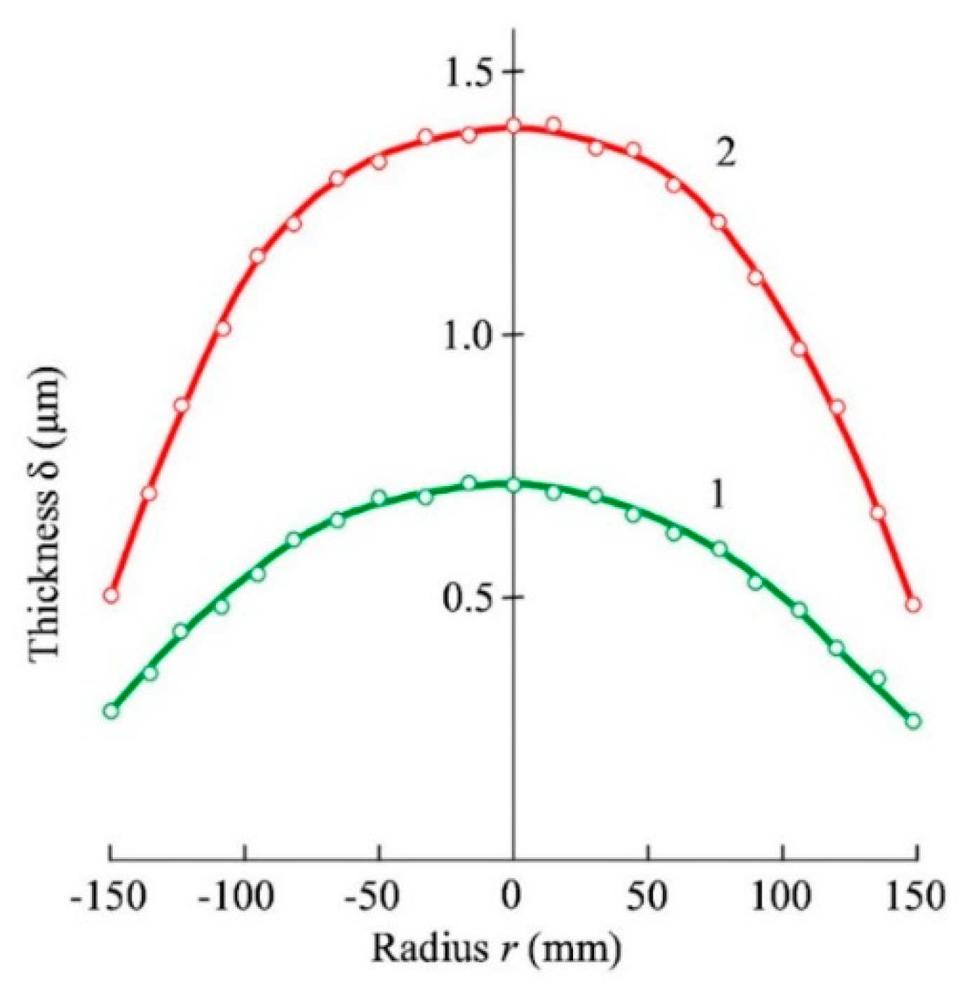
The sputtered copper atoms enter the chamber through the grid apertures and reach the glass substrate at a distance of 10 cm from the grid. First, the substrate was pretreated within 10 min by ~1 keV argon atoms. Then, a lustrous copper film was deposited on the glass substrate. Argon atoms with the energy of ~100 eV uninterruptedly bombarded the film during the deposition. Curve 1 in
Figure 6 presents the dependence of the film thickness δ on a distance
r from the substrate center. The film was deposited at zero voltage between the hollow cathode and the target, the argon pressure of
p = 0.4 Pa, and the discharge current in the anode circuit amounting to
Id = 1.8 A. The film thickness amounts to δ = 0.7 ± 0.02 μm, and the deposition rate amounts to 0.35 μm/h in the central 100 mm diameter zone. At the distance from the source axis,
r = 100 mm, the thickness diminishes to δ = 0.55 mm.
Curve 2 in
Figure 6 presents the dependence of the deposited film thickness δ on distance
r from the substrate center. The film was deposited within 40 min at the voltage between the hollow cathode and the target
Ut = 2 kV, the discharge current in the anode circuit
Id = 1.8 A, and the argon pressure
p = 0.4 Pa. The thickness amounts to δ = 1.4 ± 0.04 μm (nonuniformity less than ±3%) in the central 100 mm diameter zone, and the deposition rate amounts to 2.1 μm/h.
The investigations of the films deposited in the same conditions on glass substrates with the same sizes, but without masks on their surfaces, showed quite good adhesion of the copper film to the glass substrate of ~3 MPa at the distance r < 120 mm from the substrate center. However, the glossy surface of the substrate turns dull, and the adhesion abruptly decreases at r > 120 mm. It is due to a low flow density of fast argon ions during the substrate pretreatment.
The thickness of the sheath between the grid and the plasma emitter grows near the grid periphery [
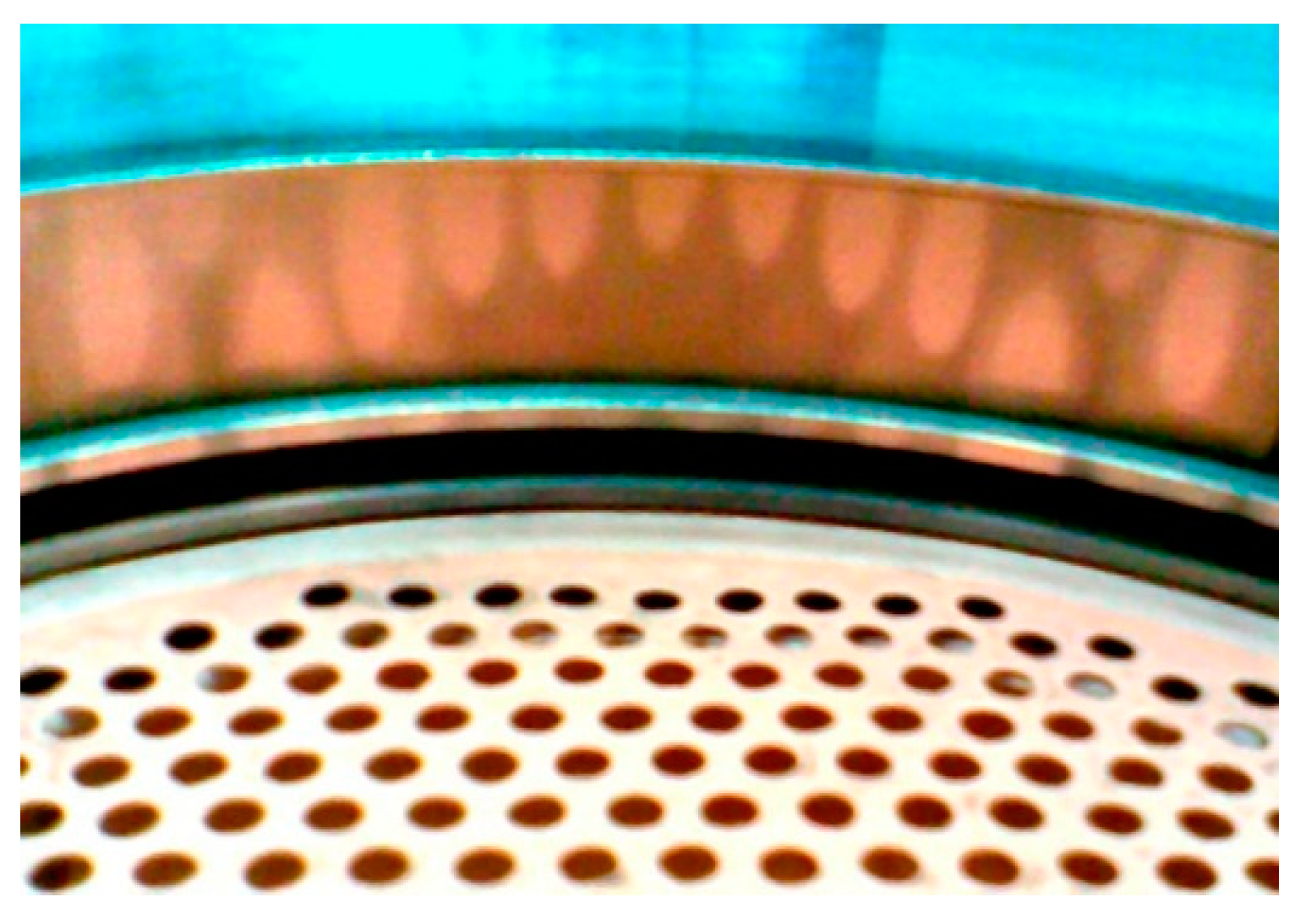
19]. Thus, the angle between the averaged velocity vector of accelerated ions passing through the grid, and the source axis also rises with the distance from the axis. The separate ion streams passing through the peripheral apertures of the grid and declining from the beam axis are narrow enough to be distinguished from each other. The number and disposition of imprints etched by the ion streams, which are on the cylindrical surface surrounding the grid (
Figure 7), match well with the disposition of the grid apertures.
The deposited film exhibits lustrous 7 mm diameter circles on a dull background, thus reproducing the grid picture when the distance between the substrate and the grid is less than 5 cm. However, the stream diameters grow several times, and the flow density of the fast argon atoms is distributed quite homogeneously, at a distance from the grid exceeding 10 cm. Thus, the whole surface of the deposited film looks like a mirror.
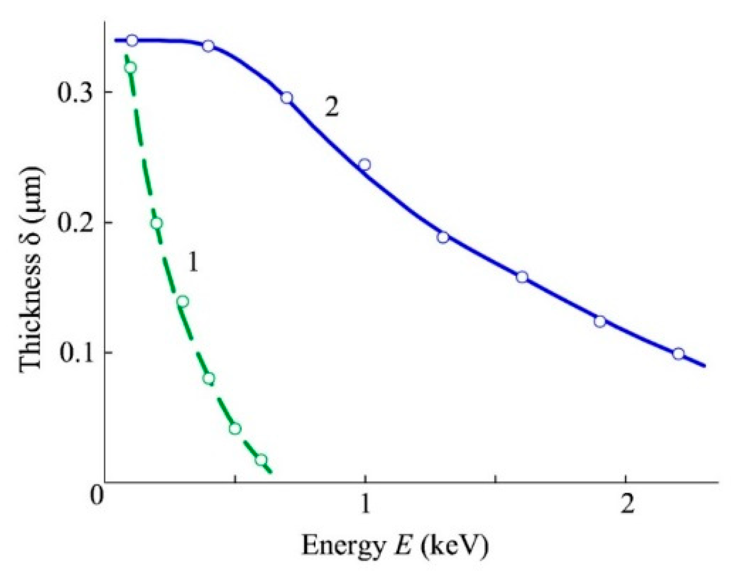
A few 48 × 60 mm
2 glass substrates covered with masks were placed, one after another, on a substrate holder at a distance of 10 cm from the source grid, to study the dependence of the film parameters on the energy of fast argon atoms. Each substrate was bombarded within 10 min with ~1 keV argon atoms at the gas pressure
p = 0.4 Pa, and current in the anode circuit of
Id = 1.8 A before the deposition. Then, the accelerating voltage was diminished, and a copper film was deposited within 2 h at zero voltage between the hollow cathode and the target, and various values of the argon atom energy
E. The dashed curve 1 in
Figure 8 represents the dependence of the copper film thickness δ on the energy
E. The film thickness decreases with an increase in their energy, and diminishes to zero at
E ~ 0.6 keV, due to sputtering by the fast argon atoms.
The full curve 2 in
Figure 8 represents the dependence of the film thickness on the fast argon energy for the copper films deposited within 20 min at the bias voltage between the hollow cathode and the target of
Ut = 2 kV. The film thickness δ ~0.34 µm is almost independent of the fast argon ion energy
E for
E < 0.4 keV. For higher argon ion energies, the film thickness monotonically decreases to 0.1 µm at
E = 2.2 keV. The data in
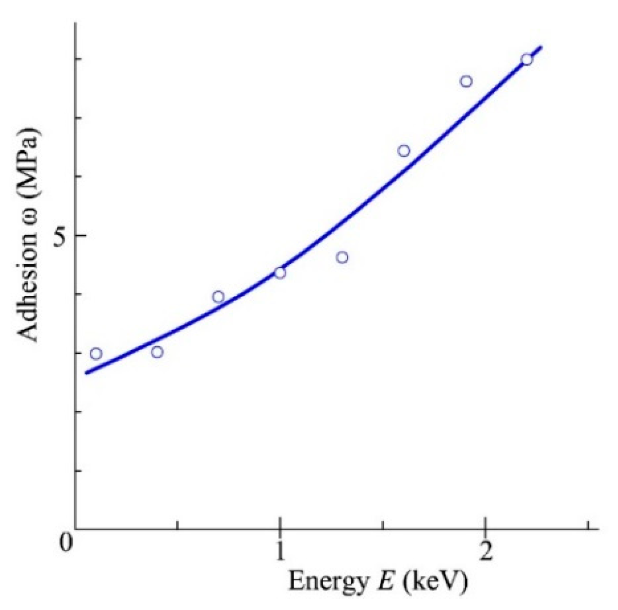
Figure 9 demonstrate a monotonic increase in the adhesion ω of the films with increasing fast atom energy
E for films deposited within 20 min at the bias voltage of
Ut = 2 kV between the hollow cathode and the target. The adhesion ω rises from ω ~3 MPa at the fast atom energy
E = 0.1 keV, up to ω ~8 MPa at
E = 2.2 keV, due to deeper penetration of the fast atoms into the substrate.
However, the increase in adhesion with the fast atom energy growth is accompanied by a substantial decrease in the deposition rate. For this reason, the continuous bombardment of the substrate and the growing film by fast argon atoms was replaced with bombardment by pulsed beams of the fast argon atoms. A 48 × 60 mm
2 substrate made of glass was first pretreated within 10 min by the argon atoms with energy of ~1 keV at the pressure
p = 0.4 Pa and the anode current of
Id = 1.8 A. Then, the voltmeter was disconnected from the anode (
Figure 1), the accelerating voltage was diminished to the minimal value of 0.2 kV, and the voltage
Ut = 2 kV was applied between the hollow cathode and the target. Finally, the pulse generator was switched on. In this case, the pulsed beams of fast argon atoms bombarded the substrate and the growing coating. Their energy was varied from 2 to 10 keV. It was shown that thickness of the films deposited within 20 min amounts to ~0.3 μm, and is almost independent of the amplitude
Uo of 40 μs-wide high-voltage pulses applied to the anode with a repetition rate of 50 Hz. Nevertheless,
Figure 10 shows that the increase in the amplitude
Uo from 2 to 9 kV results in an appreciable growth of the film adhesion ω from 7 to 20 MPa.
The important parameters of the hollow cathode sputtering system, which can be controlled for optimum deposition conditions, are listed in
Table 1, along with the symbols used in the text.
4. Discussion
At the low pressure of 0.1–1 Pa, the hollow cathode glow discharge is self-sustained, due to electrostatic confinement of electrons in the discharge plasma. This range of pressure is adequate for transportation of sputtered atoms to the substrate [
26]. The confinement is carried out only by the electric field in the cathode sheath of the discharge. It results in a high homogeneity of the discharge plasma [
27]. The same pressure range in the planar magnetron discharge is secured due to magnetic confinement of electrons. The magnetic confinement results in very inhomogeneous distributions of the plasma density and the rate of target sputtering. Thus, the use efficiency of the target material in the magnetron discharge is quite low. For example, the target weight diminished from 2.25 to 1.71 kg when the depth of the groove sputtered by ions on the surface of a 0.9-thick rectangular 15 × 37 cm
2 titanium target, used in [
28], reached 0.8 cm. It was decided to scrap the target for melting and then to install a new target because of the possible breakthrough of the thin titanium layer between the cooling water and the vacuum. Hence, in that case, the use efficiency of the target material for the film deposition amounted to 24%.
In the hollow cathode discharge, it is always possible to find a part of the cathode surface with a quite homogeneous distribution of the ion current density. For example, the distribution is very uniform in the central part of the cylindrical hollow cathode bottom. The target placed at the bottom is sputtered quite homogeneously. However, the atoms sputtered from the rest of the surface of the hollow cathode simultaneously deposit on its surface. Thus, the measured values of the target sputtering rate at the target bias voltage
Ut = 0 (dashed curve 1 in
Figure 5) can be slightly understated.
The increase in the bias voltage up to
Ut = 2 kV changes, substantially, the configuration of the sputtered atoms flow inside the hollow cathode. This results in a sixfold increase in the rate of the target sputtering and an about sixfold growth of the film deposition rate at the constant flow density of fast argon atoms to the substrate. Full curve 2 in
Figure 5 demonstrates a very high homogeneity of the target sputtering, which is unattainable for planar magnetrons. It provides a high use efficiency of the target material.
Another advantage of the hollow cathode sputtering system is the possibility to collect atoms of the sputtered target—which have not been deposited (on the substrate)—on the foils covering the cathode walls for further recycling.
Among the disadvantages of the hollow cathode sputtering system, the first that should be mentioned is the losses of the sputtered metal atoms (up to 30%) on the emissive grid, and a necessity to produce the grid and the hollow cathode of the target material to avoid contamination.
A crucial element of the hollow cathode sputtering system mentioned above is the emissive grid. It is always negative to the cathode, and prevents the fast electrons emitted by the hollow cathode from leaving it through the grid orifices. The increase in the accelerating voltage between the hollow cathode and the grid from its minimum value of 0.2 kV, up to 2 kV, allows pretreatment of the dielectric substrates by the neutral argon atoms with energy up to ~2 keV. This improves the adhesion of the films deposited afterward.
The bombardment of the substrate and the growing film by accelerated particles, at the very beginning of the film deposition, allows a further improvement of the film adhesion [
12,
13,
14]. In our case, the fast argon atoms penetrate into the substrate, into the film deposited, thereon, and mix the atoms of their materials. The penetration depth Δ is directly proportional to the argon atoms energy
E. It amounts to several nanometers at
E ~ 1 keV and tens of nanometers at
E ~ 10 keV; correspondingly. The greater the thickness Δ of the surface layer, where the atom mixing is carried out, the broader the transitional layer (interface) between the substrate and the film, and the better its adhesion. This is proven with the results presented in
Figure 10, which demonstrate a monotonic growth of the copper-to-glass adhesion from ~7 MPa at the argon atoms energy
E = 2 keV up to ~20 MPa at
E = 9 keV.
The hollow cathode sputtering system enables a simple production of pulsed beams of high-energy gas atoms by applying high-voltage pulses between its anode and its emissive grid. This allows more reliable control of the deposition process in contrast to the magnetron sputtering system, with generation of high-energy gas atoms pulsed beams [
28]. The negative high-voltage pulses are applied to a grid placed between the planar magnetron target and the substrate in the system [
28]. The fast atoms are produced there due to charge exchange collisions of accelerated ions in the sheaths of positive space charge near the grid surface. Thus, their energy distribution is continuous, and depends on the gas pressure.
The hollow cathode sputtering system produces monoenergetic gas atoms. Their energy does not depend on the gas pressure. The mean free path, λ, of argon atoms is equal to 0.067 × 10
−6 m at room temperature and atmospheric pressure
p = 10
5 Pa [
29]. At
p = 0.1 Pа, λ is approximately equal to 7 cm, and the gas density amounts to
no = 2.5 × 10
19 m
−3. Taking into account the gas heating in the discharge up to ~600 °C, and the corresponding threefold decrease in the gas density, we may suppose that, in the discharge plasma, λ ≈ 21 cm at
p = 0.1 Pa and λ ≈ 5 cm at
p = 0.4 Pa. The mean free path of accelerated ions is higher than the mean free path of the gas atoms. It exceeds the width ~1 cm of positive space charge sheaths between the plasma and the surfaces of the target, and the cathode by an order of magnitude. For this reason, the ions pass through the sheath without collisions, and bombard the target and the cathode with the kinetic energy exactly corresponding to the sheath voltage of ~400 eV on the cathode, or ~2400 eV on the target.
The density of the heated gas at
p = 0.4 Pa is equal to
no ≈ 3.33 × 10
19 m
−3. The charge exchange cross-section σ
c is decreasing, from 3 × 10
−19 to 1.3 × 10
−19 m
2 [
25], when the energy of argon ions is increasing from 0.5 to 10 keV. At the same time, the charge exchange length λ
c = 1/
noσ
c of the argon ions at the heated gas pressure
p = 0.4 Pа is increasing from 10 to 23 cm. The mean free path of fast atoms produced due to the charge exchange collisions is comparable with λ
c. For this reason, the energy of accelerated particles, arriving at the substrate placed at the distance of 10 cm from the grid, can differ slightly from the value corresponding to the accelerating voltage between the anode and the chamber. Measurements of the Doppler shift of spectral lines emitted by the fast argon atoms proved that the atoms are monoenergetic at
p = 0.4 Pа, and the losses of their kinetic energy on the 10 cm-long way to the substrate are negligible. The broadening of the spectral line emitted by the fast argon atoms and its shift to the center of the line, emitted by the slow argon atoms at higher pressures, reveals a decrease in the energy of the fast atoms due to elastic collisions with the gas atoms. An example of the fast atom energy measurements is described in [
30].
The adhesion of the films deposited at the amplitude
Uo = 2 kV of 40 μs-wide pulses applied between the anode and the grid with the repetition rate of 50 Hz is close to the adhesion of the films, which were continuously bombarded by ~2 keV argon atoms. The application of 40 μs-wide pulses cannot appreciably influence the plasma emitter density [
31]; it keeps the flow density of fast gas atoms unchanged and increases their energy. The flow density of the ~2 keV argon atoms continuously bombarding the substrate is 500 times higher than the average flow density of the ~2 keV atoms in pulsed regime. However, the increase in the flow density of the fast atoms does not practically influence the film adhesion. It results only in the unwanted and useless sputtering of the growing film (
Figure 8). The adhesion mainly depends on the energy of the fast atoms defining the thickness Δ of the surface layer, where the atoms of the substrate and the film are mixed.
5. Conclusions
The substrate pretreatment by neutral argon atoms, with kinetic energy up to 2 keV, results in production, on its surface, of structural defects, being condensation centers of the film to be grown, which ensures a sufficient adhesion of the film to the substrate.
When the fast argon atoms bombard the growing film, the film adhesion mainly depends on their energy, and monotonically grows with the increase of the energy. The pulsed bombardment does not influence the film deposition rate. However, continuous bombardment results in a dramatic reduction of the deposition rate with the increase of fast atom energy.
The electrostatic confinement of electrons in the glow discharge with the cylindrical hollow cathode and the negatively biased grid enables sputtering of the negatively biased target placed at the hollow cathode bottom at the gas pressure, which is characteristic of the planar magnetrons. The target sputtering is remarkable for the high homogeneity, which is unattainable for planar magnetrons.
The hollow cathode sputtering system, mentioned above, provides for a better use efficiency of the target material in comparison with the planar magnetrons. It allows collection of the sputtered atoms, which were not deposited on the substrate, for further recycling. Hence, the new sputtering system may be recommended for the beam-assisted deposition of expensive materials.


