Article

Effects of Air Exposure on Hard and Soft X-ray Photoemission Spectra of Ultrananocrystalline Diamond/Amorphous Carbon Composite Films

1
Department of Mechanical Engineering, Kafrelsheikh University, Kafrelsheikh 33516, Egypt
2
Department of Applied Science for Electronics and Materials, Kyushu University, Kasuga, Fukuoka 816-8580, Japan
3
Research Center for Synchrotron Light Applications, Kyushu University, Kasuga, Fukuoka 816-8580, Japan
4
Institute of Materials and Systems for Sustainability Advanced Measurement Technology Center, Nagoya University, Furo-cho, Chikusa-ku, Nagoya 464-8601, Japan
5
OSG Corporation, 2-17 Shirakumo-cho, Toyokawa-shi, Aichi 442-0018, Japan
*
Authors to whom correspondence should be addressed.
Coatings 2018, 8(10), 359; https://doi.org/10.3390/coatings8100359
Submission received: 25 August 2018 / Revised: 26 September 2018 / Accepted: 4 October 2018 / Published: 9 October 2018
(This article belongs to the Special Issue Thin Film Deposition and Characterization Techniques)

Abstract

:
Hard X-ray photoemission spectroscopy (HAXPES) was employed for the structural evaluation of ultrananocrystalline diamond/amorphous carbon (UNCD/a-C) composite films deposited on cemented carbide substrates, at substrate temperatures up to 550 °C by coaxial arc plasma deposition. The results were compared with those of soft X-ray photoemission spectroscopy (SXPES). Since nanocrystalline diamond grains are easily destroyed by argon ion bombardment, the structural evaluation of UNCD/a-C films, without the argon ion bombardment, is preferable for precise evaluation. For samples that were preserved in a vacuum box after film preparation, the sp3 fraction estimated from HAXPES is in good agreement with that of SXPES. The substrate temperature dependencies also exhibited good correspondence with that of hardness and Young’s modulus of the films. On the other hand, the sp3 fraction estimated from SXPES for samples that were not preserved in the vacuum box had an apparent deviation from those of HAXPES. Since it is possible for HAXPES to precisely estimate the sp3 fraction without the ion bombardment treatment, HAXPES is a feasible method for UNCD/a-C films, comprising nanocrystalline diamond grains.

Graphical Abstract

1. Introduction

Nanocrystalline diamond (NCD) films have shown promise as a hard coating material for enhancing the performance of cutting tools and prolonging tool lifetime. NCD films introduce the highest known hardness, a smooth surface, and a low friction coefficient, resulting in fine diamond grains, less than 100 nm in size [1,2,3]. Ultrananocrystalline diamond (UNCD) films, a kind of NCD film comprising grains less than 10 nm [4,5], are a promising candidate as a hard coating application on cutting tools [6].
Precisely, UNCD films comprise a large number of nano-sized diamond grains, an amorphous carbon matrix [7], and a large number of structurally specific grain boundaries in the films. They are prepared by microwave plasma CVD [8,9] and coaxial arc plasma deposition (CAPD) [10,11,12,13,14]. When CAPD is used, film deposition is possible in hydrogen-free atmospheres, which results in films containing a greater amount of nonhydrogenated amorphous carbon (a-C), compared with those prepared by CVD. Thus, when prepared with CAPD, we distinctively describe them as UNCD/a-C films.
It is well known that cathodic arc discharge deposition makes possible the growth of hydrogen-free sp3-rich a-C films [15]. In addition, CAPD also has the unique feature where a coaxial arc plasma gun equipped with an anodic cylinder can bunch ions ejected from a cathodic graphite rod located in the cylinder. Owing to this structure, a supersaturated condition with highly energetic carbon ions, desired for the growth of UNCD crystallites [14], can be realized on substrates [16,17]. The high hardness of UNCD/a-C films is attributed to the existence of UNCD crystallites and the sp3-rich a-C matrix [18].
Careful characterization of the atomic structures is essential since the sp3 fraction determines the mechanical properties of carbon films. The sp3 fraction is estimated by various methods, such as Raman spectroscopy, soft and hard X-ray photoemission spectroscopy, Auger electron spectroscopy, near edge X-ray absorption fine structure (NEXAFS), and high energy electron loss spectroscopy (HEELS).
Among the methods of sp3 characterization, Raman spectroscopy is a popular optical technique used to investigate bonding structures of carbon films. Although, there has been a debate regarding the accuracy of identifying the UNCD crystallites using this method [19,20] and it can’t estimate the sp3 fraction precisely [21]. While the NEXAFS and HEELS techniques are available for analyzing bonding structures, they also show some uncertainty in estimating the sp3 fraction [22].
For the X-ray photoemission spectroscopic characterization of UNCD/a-C films, the influence of surface condition of the films spectra, is not negligible [23]. The soft X-ray photoemission spectroscopy (SXPES), employed mainly for investigating the atomic structures of carbon films [24], detects photoelectrons ejected from surfaces a few nanometers in depth. Thus, to exclude the influence of surface conditions, surface contaminants are removed with ion bombardments before measurement. When applied to UNCD/a-C films, nano-sized diamond crystallites are easily destroyed by the bombardment of Argon ions and it is therefore difficult to evaluate the original structure around the film surfaces [23].
Hard X-ray photoemission spectroscopy (HAXPES) has attracted attention in recent years as an alternative technique that solves the above-mentioned problem, as it examines buried regions at depths of more than 10 nm by employing hard X-ray incidence beams. In other words, it detects spectra mainly from bulk electronic structures on the films subsurface [25,26]. In this work, HAXPES was applied to the structural evaluation of UNCD/a-C films and correlations between the mechanical and structural properties were studied. In addition, HAXPES results were compared to those of SXPES and the feasibility of HAXPES for the evaluation of UNCD/a-C films was investigated.

2. Materials and Methods

2.1. Film Preparation

UNCD/a-C films were deposited on WC-Co substrates (K-type cemented tungsten carbide) with dimensions of ϕ10 × 4.5 mm by CAPD, employing a coaxial arc plasma gun (APG-1000, ULVAC, kanagawa, Japan) equipped with a graphite rod (purity of 99.99%, ϕ10 × 30 mm). The pretreatment of the WC-Co substrates by chemical etching for removing Co near the surface, which has been indispensably applied for the hard coating of polycrystalline diamond on WC-Co by CVD, was not carried out in this study. Only the pretreatment of roughening the WC-Co surface was made in the range of Ra = 0.15 µm to 0.2 µm, by dissolving the WC using chemical etching to enhance adhesion of the films. Before the deposition of the films, the inside of the vacuum chamber was evacuated to be less than 10−4 Pa by a turbomolecular pump. A voltage of 100 V was applied to the coaxial arc plasma gun equipped with a 720 μF capacitor and the arc discharge of the arc plasma gun was operated at a repetition rate of 1 Hz. The films were deposited at different substrate temperatures ranging from room temperature to 550 °C. The details of film preparation conditions are presented in our previous papers [15,16].

2.2. Film Characterization

The samples were divided into two groups according to a difference in the storage procedure after deposition. The difference is schematically shown in Figure 1. The samples of Group I were exposed naturally to surrounding air for a maximum of two weeks after finishing deposition by CAPD apparatus and until HAXPES and SXPES measurements were made. On the other hand, the samples of Group II were preserved in a portable vacuum box containing silica gel, where the inside pressure is less than 0.1 MPa, as soon as they were taken out of the CAPD apparatus, for a maximum of two weeks. Moreover, they were quickly set into an SXPES vacuum apparatus before measurements were taken.
The atomic structures of the films were examined by HAXPES and SXPES. While, HAXPES was applied to the samples of Group I, SXPES investigated the samples of Group I and II. The chemical compositions and sp3/(sp3 + sp2) ratio were investigated from SXPES and HAXPES spectra. The HAXPES measurements with an incident photon energy of 8 keV were conducted at BL47XU in Spring-8. SXPES measurements with an incident photon energy of 350 eV were performed at BL12 of SAGA Light Source/Kyushu Synchrotron Light Source Center. In addition, SXPES wide-range measurements with a photon energy of 1253.6 eV (Mg Kα line) were made for investigating the chemical composition of the films. The spectra were decomposed into peaks using a Voigt function (80% Gaussian and 20% Lorentzian) after subtracting backgrounds [27].
Each sample was tested ten times to calculate mean values of hardness and Young’s modulus by nano-indentation test at an applied load of 0.5 mN (HM500, Fisher Instruments Company, Sindelfingen, Germany).

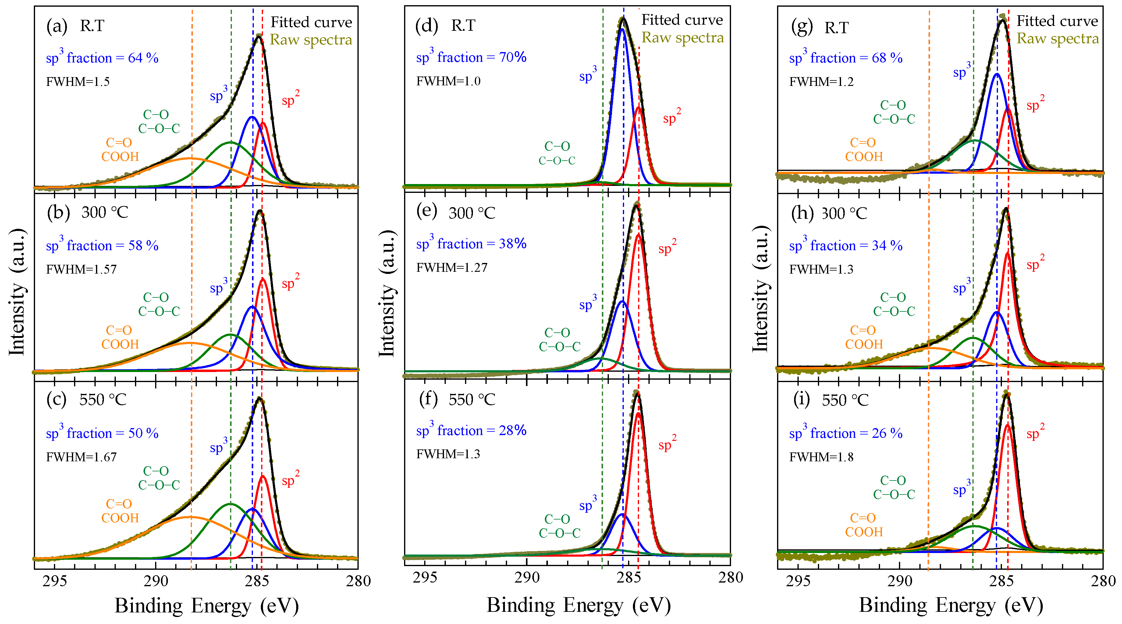
3. Results and Discussions

Table 1 indicates the hardness and Young’s modulus of films deposited at different substrate temperatures. The hardness and Young’s modulus decrease with increasing substrate temperature, which implies that the atomic structures of films are affected by the increase in substrate temperature. To study the origin, SXPES and HAXPES were employed.
Figure 2 shows the SXPES and HAXPES survey-spectra. The spectra do not show any peaks due to substrate elements, which means that the diffusion from substrates into films rarely occurs, even at the highest substrate temperature of 550 °C [15]. They show only significant intense C 1s peaks and weak O 1s peaks from collected photoelectrons of excited core levels of carbon and oxygen elements. The O 1s peak at 532 eV is mainly ascribed to the adsorbed oxygen on the surface of the film [28]. The HAXPES O 1s peaks are obviously weak comparing with those of the SXPES O 1s peaks. In addition, the HAXPES detects spectra mainly from bulk electronic structures at buried layers of the films [29]. This means that the O 1s peak is partially attributed to residual oxygen in the chamber, resulted from water vapor contamination during the films deposition.
Figure 3 shows the C 1s spectra of Group I samples (a), (b), and (c), measured by SXPES and (d), (e), and (f), measured by HAXPES, and Group II samples (g), (h), and (i), measured by SXPES. Macroscopically, the maximum energy of the spectra shifts to a higher binding energy with decreasing substrate temperature, which is particularly evident for Group I spectra measured by HAXPES and Group II spectra measured by SXPES. The shifts might have occurred due to the enhancement of the sp3 bonding fraction [30], which is consistent with hardness increasing as substrate temperature decreases.
To analyze spectra precisely, they were decomposed into the following four peaks: sp2-bonded carbon (C=C), sp3-bonded carbon (C–C), carbon-oxygen single bonds (C–O/C–O–C), and carbon-oxygen double bonds (C=O/COOH) [31,32]. The peak centers were aligned at the same difference of binding energy to precisely compare the samples measured by SXPES. The C–O/C–O–C peaks should be ascribed to the adsorption of oxygen on the film surface during and after films deposition [23,33]. The C=O/COOH peak is observed in the spectra measured by SXPES for Group I samples. This should be observed because SXPES preferentially detects the top layers of film surface and is easily altered by surface contaminants. Group II samples showed weakened C=O/COOH peaks in their spectra, which means the adsorption of oxygen is suppressed, owing to their preservation in the portable vacuum box. The vacuum box contains powdered silica gel that absorbs humidity and keeps the inside of the vacuum box dry. This means that the contribution of contaminants found in the upper first layers of the films is limited, due to preserving the samples in the vacuum box. The HAXPES measurements show sharp spectra with very weak shoulder of the C–O/C–O–C peak, due to investigation at deep depth in the films. However, the argon ion bombardment is essential for cleaning the films surface prior to X-ray photoemission spectroscopic measurements, to reduce the contribution of film surface contaminants. The HAXPES method makes possible the structural examination of the UNCD/a-C films without applying any surface pretreatment, such as argon ion bombardment, which destroys nano-sized diamond crystallite in the films [23].
The sp3 peaks show a relative decrease as substrate temperature increases. The HAXPES technique produces sharp and intense sp3 peaks with a noticeable difference compared to the sp2 peaks, unlike those obtained by SXPES for Group I samples. The Group II samples preserved in the vacuum box produced relatively consistent peaks, compared to those revealed by HAXPES. Figure 4 shows the substrate temperature dependence of the hardness and sp3 bonding fraction. The dependence profile of the sp3 bonding fraction estimated from HAXPES and SXPES for Group II samples are in good agreement, not only with each other but also with the hardness dependence profile. This means that the estimation of the sp3 fraction is precise, since the hardness proportionally increases with the sp3 fraction [34,35]. On the other hand, the substrate temperature dependence profile of the sp3 fraction estimated from SXPES for Group I, obviously deviates from that of hardness. Estimation of the sp3 bonding fraction is also affected by the existence of C–O/C–O–C and C=O/COOH peaks. The SXPES investigation for Group I emphasizes that the presence of undesirable contaminants on the films surface could lead to difficulties in obtaining surface functionalization. Therefore, the HAXPES method and demonstrating a careful methodology for SXPES investigation, are recommended when assessing the sp3 bonding fraction to UNCD/a-C films and nanomaterials.

4. Conclusions

The atomic structures of UNCD/a-C composite films were investigated by HAXPES and SXPES. It was found that the sp3 fraction estimated from HAXPES spectra corresponds well with the hardness and Young’s modulus in their substrate temperature dependencies. On the other hand, the sp3 fraction estimated from SXPES spectra of the samples that were exposed to air after film preparation deviated from that of HAXPES, while SXPES results of samples that were preserved in the vacuum box were in good agreement with those of HAXPES. This indicates that it is possible for HAXPES to precisely estimate the sp3 fraction and similarly to SXPES when samples are preserved in a vacuum box. HAXPES is a promising technique for structural characterization of UNCD/a-C films because the condition of the film surface has a negligible effect on the spectra of films.

Author Contributions

Writing-Original Draft Preparation, M.E.; Methodology, M.E.; Formal Analysis, M.E.; Visualization, M.E.; Structural Investigation, H.N., A.T., K.H., K.K., T.S., and E.I., Mechanical Investigation, K.M., H.G., and M.S.; Writing-Review & Editing, T.Y.; Supervision, T.Y.; Project Administration, T.Y.; Funding Acquisition, T.Y.

Funding

This research was partially funded by Osawa Scientific Studies Grants Foundation, Advanced Machining Technology and Development Association, and JST A-STEP Stage II (seed development type AS2915051S).

Acknowledgments

The first author acknowledges the financial assistance to study a Ph.D. at Kyushu University provided by the Egyptian government. The XPS measurements were performed at BL 12 of Kyushu Synchrotron Light Research Center/Saga Light Source (Proposal Nos, 1410105S, 1607062S, and 1610090S). The HAXPES investigations were conducted at BL47XU in SPring-8 (Proposal No. 2014B1426).

Conflicts of Interest

The authors declare no conflict of interest.

References

  1. Aslantas, K.; Hopa, H.E.; Percin, M.; Ucun, I.; Çicek, A. Cutting performance of nano-crystalline diamond (NCD) coating in micro-milling of Ti6Al4V alloy. Precis. Eng. 2016, 45, 55–66. [Google Scholar] [CrossRef]
  2. Schwarzbach, D.; Haubner, R.; Lux, B. Internal stresses in CVD diamond layers. Diam. Relat. Mater. 1994, 3, 757–764. [Google Scholar] [CrossRef]
  3. Li, H.; Sheldon, B.W.; Kothari, A.; Ban, Z.; Walden, B.L. Walden. Stress evolution in nanocrystalline diamond films produced by chemical vapor deposition. J. Appl. Phys. 2006, 100, 094309. [Google Scholar] [CrossRef]
  4. Liao, W.-H.; Lin, C.-R.; Wei, D.-H. Effect of CH4 concentration on the growth behavior, structure, and transparent properties of ultrananocrystalline diamond films synthesized by focused microwave Ar/CH4/H2 plasma jets. Appl. Surf. Sci. 2013, 270, 324–330. [Google Scholar] [CrossRef]
  5. Gruen, D.M. Nanocrystalline diamond films. Annu. Rev. Mater. Sci. 1999, 29, 211–259. [Google Scholar] [CrossRef]
  6. Bhattacharyya, S.; Auciello, O.; Birrell, J.; Carlisle, J.; Curtiss, L.; Goyette, A.; Gruen, D.; Krauss, A.; Schlueter, J.; Sumant, A. Synthesis and characterization of highly-conducting nitrogen-doped ultrananocrystalline diamond films. Appl. Phys. Lett. 2001, 79, 1441–1443. [Google Scholar] [CrossRef]
  7. Wiora, M.; Brühne, K.; Flöter, A.; Gluche, P.; Willey, T.; Kucheyev, S.; Van Buuren, A.; Hamza, A.; Biener, J.; Fecht, H.-J. Grain size dependent mechanical properties of nanocrystalline diamondfilms grown by hot-filament CVD. Diam. Relat. Mater. 2009, 18, 927–930. [Google Scholar] [CrossRef]
  8. Xiao, X.; Birrell, J.; Gerbi, J.; Auciello, O.; Carlisle, J. Low temperature growth of ultrananocrystalline diamond. J. Appl. Phys. 2004, 96, 2232–2239. [Google Scholar] [CrossRef]
  9. Manawi, Y.M.; Samara, A.; Al-Ansari, T.; Atieh, M.A. A Review of Carbon Nanomaterials’ Synthesis via the Chemical Vapor Deposition (CVD) Method. Materials 2018, 11, 822. [Google Scholar] [CrossRef] [PubMed]
  10. Hanada, K.; Yoshitake, T.; Nishiyama, T.; Nagayama, K. Time-resolved spectroscopic observation of deposition processes of ultrananocrystalline diamond/amorphous carbon composite films by using a coaxial arc plasma gun. Jpn. J. Appl. Phys. 2010, 49, 08JF09. [Google Scholar] [CrossRef]
  11. Naragino, H.; Egiza, M.; Tominaga, A.; Murasawa, K.; Gonda, H.; Sakurai, M.; Yoshitake, T. Hard coating of ultrananocrystalline diamond/nonhydrogenated amorphous carbon composite films on cemented tungsten carbide by coaxial arc plasma deposition. Appl. Phys. A 2016, 122, 761. [Google Scholar] [CrossRef]
  12. Naragino, H.; Egiza, M.; Tominaga, A.; Murasawa, K.; Gonda, H.; Sakurai, M.; Yoshitake, T. Room-temperature hard coating of ultrananocrystalline diamond/nonhydrogenated amorphous carbon composite films on tungsten carbide by coaxial arc plasma deposition. Jpn. J. Appl. Phys. 2016, 55, 030302. [Google Scholar] [CrossRef]
  13. Casiraghi, C.; Robertson, J.; Ferrari, A.C. Diamond-like carbon for data and beer storage. Mater. Today 2007, 10, 44–53. [Google Scholar] [CrossRef]
  14. Inspektor, A.; Bauer, C.; Oles, E. Superhard coatings for metal cutting applications. Surf. Coat. Technol. 1994, 68, 359–368. [Google Scholar] [CrossRef]
  15. Chhowalla, M.; Davis, C.; Weiler, M.; Kleinsorge, B.; Amaratunga, G. Stationary carbon cathodic arc: Plasma and film characterization. J. Appl. Phys. 1996, 79, 2237–2244. [Google Scholar] [CrossRef]
  16. Liu, D.; Benstetter, G.; Lodermeier, E.; Zhang, J.; Liu, Y.; Vancea, J. Filtered pulsed carbon cathodic arc: Plasma and amorphous carbon properties. J. Appl. Phys. 2004, 95, 7624–7631. [Google Scholar] [CrossRef]
  17. Chhowalla, M.; Robertson, J.; Chen, C.; Silva, S.; Davis, C.; Amaratunga, G.; Milne, W. Influence of ion energy and substrate temperature on the optical and electronic properties of tetrahedral amorphous carbon (ta-C) films. J. Appl. Phys. 1997, 81, 139–145. [Google Scholar] [CrossRef] [Green Version]
  18. Naguib, N.N.; Elam, J.W.; Birrell, J.; Wang, J.; Grierson, D.S.; Kabius, B.; Hiller, J.M.; Sumant, A.V.; Carpick, R.W.; Auciello, O. Enhanced nucleation, smoothness and conformality of ultrananocrystalline diamond (UNCD) ultrathin films via tungsten interlayers. Chem. Phys. Lett. 2006, 430, 345–350. [Google Scholar] [CrossRef]
  19. Hara, T.; Nojiri, Y.; Hanada, K.; Yoshitake, T. Detection methods of diamond diffraction peaks in ultrananocrystalline diamond/amorphous carbon composite films by X-ray diffraction measurement with semiconductor counter detector. Jpn. J. App. Phys. 2015, 54, 108002. [Google Scholar] [CrossRef]
  20. Ferrari, A.; Robertson, J. Origin of the 1150 cm−1 Raman mode in nanocrystalline diamond. Phys. Rev. B 2001, 63, 121405. [Google Scholar] [CrossRef]
  21. De Bonis, A.; Rau, J.; Santagata, A.; Teghil, R. Diamond-like carbon thin films produced by femtosecond pulsed laser deposition of fullerite. Surf. Coat. Technol. 2011, 205, 3747–3753. [Google Scholar] [CrossRef]
  22. Diaz, J.; Paolicelli, G.; Ferrer, S.; Comin, F. Separation of the sp3 and sp2 components in the C1s photoemission spectra of amorphous carbon films. Phys. Rev. B 1996, 54, 8064. [Google Scholar] [CrossRef]
  23. Ohmagari, S.; Yoshitake, T.; Nagano, A.; Ohtani, R.; Setoyama, H.; Kobayashi, E.; Nagayama, K. X-ray photoemission spectroscopic study of ultrananocrystalline diamond/hydrogenated amorphous carbon composite films prepared by pulsed laser deposition. Diam. Relat. Mater. 2010, 19, 911–913. [Google Scholar] [CrossRef]
  24. Haerle, R.; Riedo, E.; Pasquarello, A.; Baldereschi, A. sp2/sp3 hybridization ratio in amorphous carbon from C 1s core-level shifts: X-ray photoelectron spectroscopy and first-principles calculation. Phys. Rev. B 2001, 65, 045101. [Google Scholar] [CrossRef]
  25. Ouardi, S.; Fecher, G.H.; Felser, C. Bulk electronic structure studied by hard X-ray photoelectron spectroscopy of the valence band: The case of intermetallic compounds. J. Elec. Spec. Relat. Phenom. 2013, 190, 249–267. [Google Scholar] [CrossRef]
  26. Claessen, R.; Sing, M.; Paul, M.; Berner, G.; Wetscherek, A.; Müller, A.; Drube, W. Hard x-ray photoelectron spectroscopy of oxide hybrid and heterostructures: A new method for the study of buried interfaces. New J. Phys. 2009, 11, 125007. [Google Scholar] [CrossRef]
  27. Yoshitake, T.; Nagano, A.; Ohmagari, S.; Itakura, M.; Kuwano, N.; Ohtani, R.; Setoyama, H.; Kobayashi, E.; Nagayama, K. Near-Edge X-ray Absorption Fine-Structure, X-ray Photoemission, and Fourier Transform Infrared Spectroscopies of Ultrananocrystalline Diamond/Hydrogenated Amorphous Carbon Composite Films. Jpn. J. Appl. Phys. 2009, 48, 020222. [Google Scholar] [CrossRef]
  28. Coşkun, Ö.D.; Zerrin, T. Optical, structural and bonding properties of diamond-like amorphous carbon films deposited by DC magnetron sputtering. Diam. Relat. Mater. 2015, 56, 29–35. [Google Scholar] [CrossRef]
  29. Woicik, J.C. Hard X-ray Photoelectron Spectroscopy (HAXPES); Springer: Berlin, Germany, 2016; pp. 111–140. [Google Scholar]
  30. Merel, P.; Tabbal, M.; Chaker, M.; Moisa, S.; Margot, J. Direct evaluation of the sp3 content in diamond-like-carbon films by XPS. Appl. Surf. Sci. 1998, 136, 105–110. [Google Scholar] [CrossRef]
  31. Kaciulis, S. Spectroscopy of carbon: From diamond to nitride films. Surf. Interface Anal. 2012, 44, 1155–1161. [Google Scholar] [CrossRef]
  32. Dwivedi, N.; Kumar, S.; Malik, H.; Rauthan, C.; Panwar, O. Correlation of sp3 and sp2 fraction of carbon with electrical, optical and nano-mechanical properties of argon-diluted diamond-like carbon films. Appl. Surf. Sci. 2011, 257, 6804–6810. [Google Scholar] [CrossRef]
  33. Ren, Y.; Ding, Z.; Wang, C.; Zang, C.; Zhang, Y.; Xu, L. Influence of DBD plasma pretreatment on the deposition of chitosan onto UHMWPE fiber surfaces for improvement of adhesion and dyeing properties. Appl. Surf. Sci. 2017, 396, 1571–1579. [Google Scholar] [CrossRef]
  34. Tunmee, S.; Supruangnet, R.; Nakajima, H.; Zhou, X.; Arakawa, S.; Suzuki, T.; Kanda, K.; Ito, H.; Komatsu, K.; Saitoh, H. Study of Synchrotron Radiation Near-Edge X-ray Absorption Fine-Structure of Amorphous Hydrogenated Carbon Films at Various Thicknesses. J. Nanomater. 2015, 16, 414. [Google Scholar] [CrossRef]
  35. Suschke, K.; Hübner, R.; Murmu, P.P.; Gupta, P.; Futter, J.; Markwitz, A. High energy radial deposition of diamond-like carbon coatings. Coatings 2015, 5, 326–337. [Google Scholar] [CrossRef]
Figure 1. Schematic diagram of the experimental procedures.
Coatings 08 00359 g001
Figure 2. Soft X-ray photoemission spectroscopic (SXPES) survey (ad), and hard X-ray photoemission spectroscopic (HAXPES) survey (eh), of Group I ultrananocrystalline. diamond/amorphous carbon (UNCD/a-C) films deposited at substrate temperature of room temperature (R.T.), 300 °C, and 550 °C, and WC-Co substrate.
Coatings 08 00359 g002
Figure 3. C 1s SXPES (ac), and C 1s HAXPES (df), of Group I and C 1s SXPES (gi), of Group II UNCD/a-C films deposited at substrate temperature of R.T. 300 °C and 550 °C.
Coatings 08 00359 g003
Figure 4. (Color online) Correlation between the hardness and the estimated sp3/(sp3 + sp2) amount ratio of UNCD/a-C films as a function of substrate temperature.
Coatings 08 00359 g004
Table 1. Typical preparation conditions of the UNCD/a-C films.
Preparation ConditionsSample 1Sample 2Sample 3
Substrate temp. (°C)Room temp. (R.T.)300550
Deposition rate (nm/pulse)0.290.350.35
Hardness (GPa)51.321.211.7
Young’s Modulus (GPa)520.2271.1121.9

