1. Introduction
A need for an AR coating for high-power fused-silica Q-switch components centered at 1064 nm with the ability to survive 20 J/cm2 prompted this small study to determine the material dependence on the absorption by the photothermal common-path interferometry (PCI) method and a laser-induced damage threshold (LIDT). In Phase 1 of the study, single layers circa 500 nm were grown and characterized by spectrophotometric transmission, PCI, and where possible, LIDT. Phase 2 incorporated these materials into double-layer anti-reflection (AR) designs, and a comparison is then made between their single-layer values and those of the subsequent double layer. All coatings were grown at Helia Photonics Ltd. on various substrates, including silicon, Borofloat 33, and Spectrosil 2000 glass witness samples, and, in the case of a few designs, on final fused-silica Q-switch components. LIDT measurements were carried out by Lidaris Ltd. (Vilnius, Lithuania) on the witness samples and for the larger components at Quantel Inc. (Bozeman, MT, USA). PCI measurements were measured at the Ginzton Lab at Stanford University, and atomic force microscopy (AFM) was used in conjunction with an optical Nomarski assessment at the University of Glasgow. Additional optical measurements including ellipsometric and spectrophotometric assessments were carried out at the University of the West of Scotland.
2. Coating Deposition Techniques and Materials
Thin-film coatings were grown using various deposition systems at Helia Photonics, Scotland, mainly built in-house. The deposition techniques used in this trial were an ion-assisted electron beam (ebeam) with thermal evaporation, radio frequency (RF) sputtering, pulsed direct-current (DC) magnetron sputtering, and thermal evaporation only. An AR coating design was used for all samples and coated on both sides of silica-based substrates including Spectrosil 2000, used for PCI absorption and AFM measurement, and Borofloat 33, used for the LIDT measurements. The substrates were ultrasonically cleaned with an identical solvent process prior to coating to ensure minimal surface contamination. A description of the deposition techniques used and their associated parameters is given in
Table 1.
Each coating sample had a material composition chosen due to a variety of practical use scenarios, and the target materials and techniques available at the time of deposition. A description of each coating composition and deposition techniques is given in
Table 2. The transmission measurements are also given and were made with a Perkin Elmer Lambda 900 spectrophotometer.
3. PCI Optical Absorption Measurements
The PCI measurement technique was used to measure the optical absorption of the coatings and is based on measuring the thermal lensing caused by the pump beam (CW, λ = 1064 nm, up to 8 W, spot size = 65 μm) and the resulting interference from the phase mismatch between the central and outermost part of the probe beam (CW, λ = 632 nm, 2.5 mW, spot size = 110 μm). The pump and probe beams cross in the same plane at an angle of 9°, providing an interaction length of 3 mm.
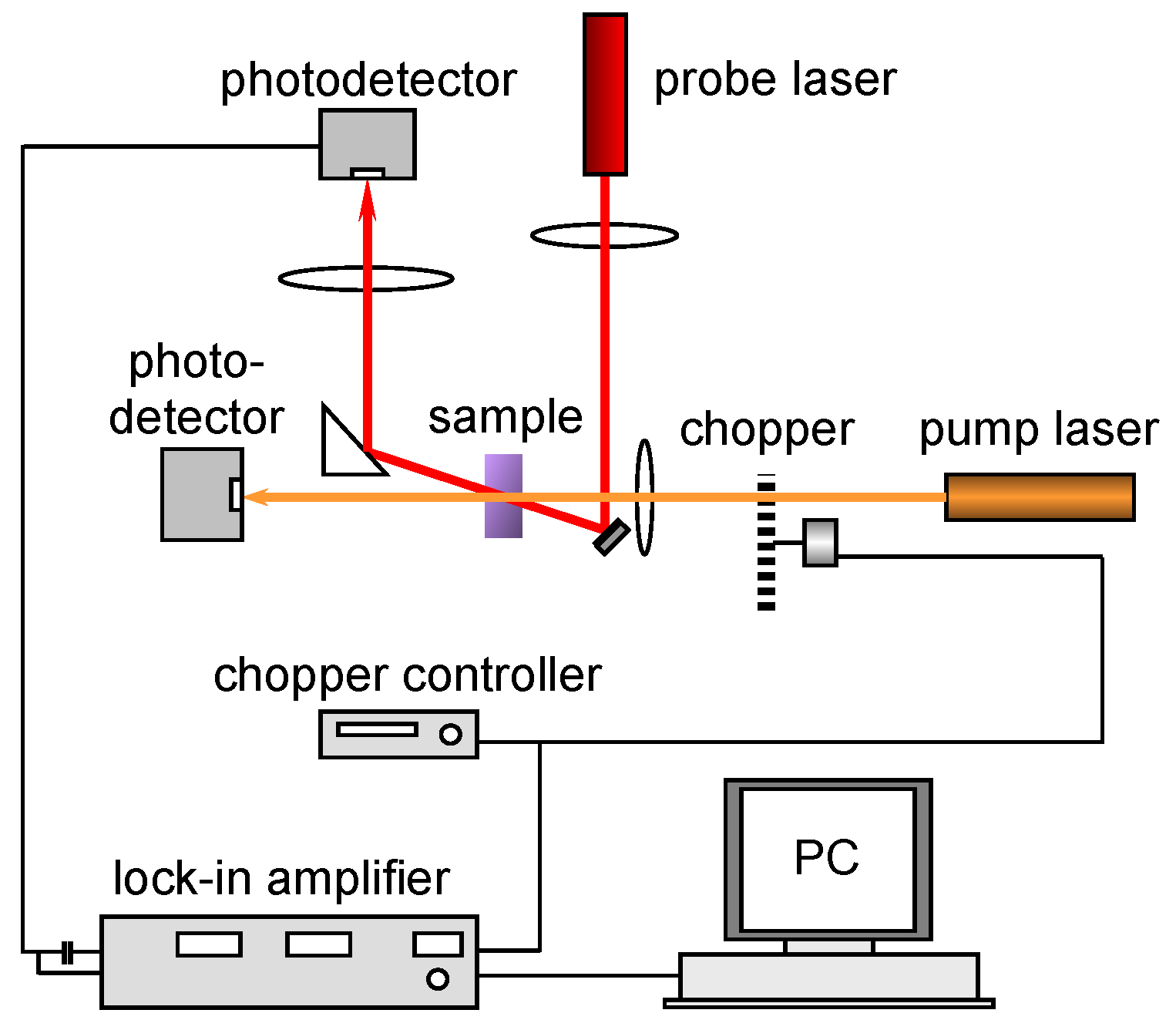
A schematic of the PCI experimental setup is shown in
Figure 1. The detected AC voltage (
VAC) signal is comprised of only first-order terms and hence can be normalized to the total probe power (DC output voltage (
VDC) of the detector) over that of the independent pump power (
Wpump). Thus, the value of the absorption loss, α, is simply proportional to the ratio
VAC/VDC/Wpump. The setup was calibrated using a Newport metallic neutral density filter, which had an absorption of 22% at 1064 nm (measured with a Cary 500 spectrophotometer). With these parameters, an optical absorption at 1064 nm of α = 0.02 ppm can be measured using pump powers up to 8.0 W. Further details of the measurement setup and process can be found in [
1,
2,
3].
The recorded signal is read from the crossing point of the pump and probe beams that move along the pump propagation direction, i.e., perpendicular to the coating in the z-direction (z-scan) or across the coating in the x-direction (x-scan).
In order to ensure the absorption of the coatings is easily distinguishable from the substrate, it is preferable to have a substrate with low absorption compared to the applied coating. The absorption of a sample of Borofloat 33 and Spectrosil 2000 was studied as candidate substrate materials. The Borofloat 33 gave an average α = 2200 ppm/cm with an uneven spread of the PCI signal. The Spectrosil 2000 was chosen as the substrate for the subsequent PCI absorption measurements on the coating samples, as it gave a relatively low and uniform α = 19.5 ppm/cm, as shown in
Figure 2.
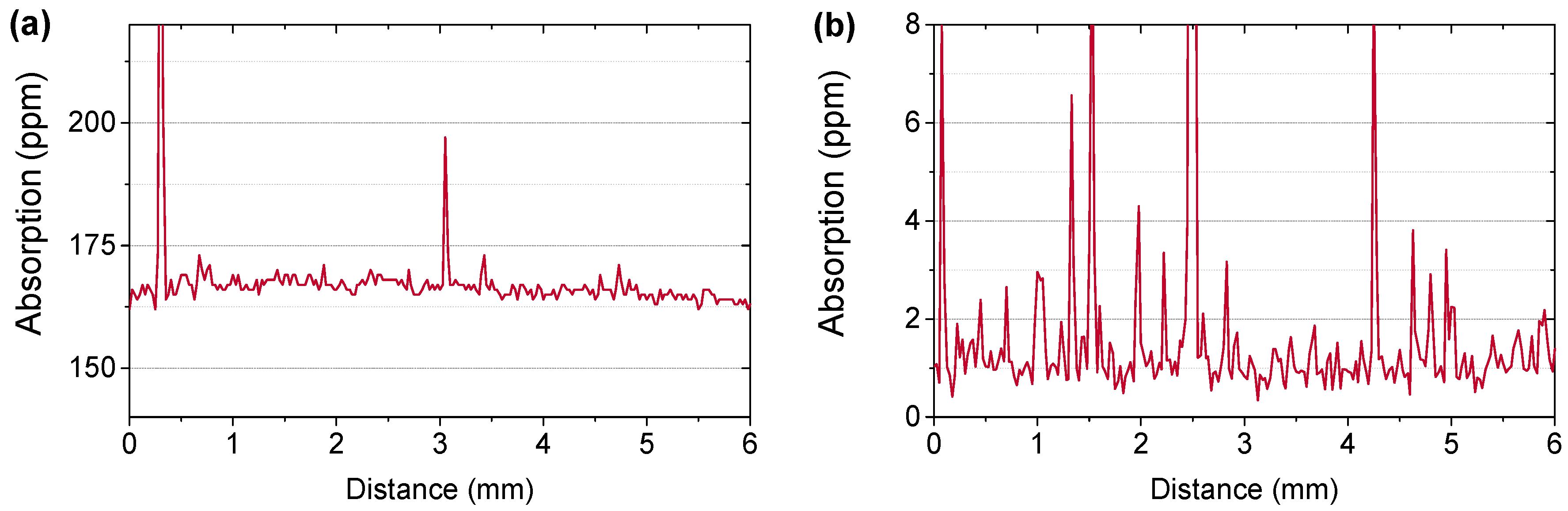
PCI x-scans highlighting the best and worst coating absorption values for the ZrO
2 and LiF coating samples are shown in
Figure 3. The x-scans probe the absorption across a 6-mm line on the coating.
Figure 3a shows the absorption of the single-layer ZrO
2 sample, with a baseline α = 168 ppm, which was the highest single-layer absorption measured. The best single-layer absorption was from the LiF coating (x-scan shown in
Figure 3b) with a baseline α = 1 ppm. Spikes in the data may be due to defects such as non-stoichiometric regions, absorbing impurities, and surface contamination; although care is taken to ensure the coating surface is clean and free of any dust during measurement. The baseline PCI absorption values for all of the single-layer coatings studied are given in
Table 3, and the absorption is also given in ppm/nm for comparison.
For the test AR coatings, the ZrO
2/SiN x-scan shown in
Figure 4a shows several spikes, with a baseline α = 57 ppm. By comparison,
Figure 4b shows the ZrO
2/SiO
2 sample, which has a lower baseline α = 9 ppm, and relatively few spikes, indicating a uniform and high-quality coating. The baseline absorption measurements for all of the AR coatings are also given in
Table 4.
4. Laser-Induced Damage Threshold and Material Properties
Laser-induced damage threshold was assessed at two facilities: Lidaris Ltd. and Quantel Inc. Lidaris used the first harmonic of pulsed Nd:YAG InnoLas Laser: SpitLight Hybrid laser (λ = 1064 nm, linear polarization, TEM00 single mode, pulse duration 9.6 ns ± 1 ns), λ/2 plate combined with additional polarizer attenuator, online scattered light damage detection, and offline inspection of damage detection using Nomarski microscopy (×100). For each sample, 411 equally spaced test sites in square grid pattern were used to reduce erratic defect-driven results and assess the threshold. The beam diameter in the target plane (1/e2) was 203.6 μm. Quantel used a Q-Switched laser (λ = 1064 nm, linear polarization, TEM00 single mode, pulse duration 20 ns) with a beam diameter (1/e2) of 560.0 μm, 80 test sites per sample. In accordance with the end-specification, Quantel tests were only carried out at 200-on-1.
The coating samples were tested in 1-on-1 and s-on-1 (
s = 200, 1000) regimes, these are defined within the ISO 11254-1 and 11254-2 standards [
4,
5]. Where strong differences between each test regime exist, it is expected that the coating undergoes significant parametric change during the test, such as localized annealing and stoichiometric balancing (for example, previously unpublished internal work shows the average stoichiometry of tantalum oxide as being Ta
2.5O
5).
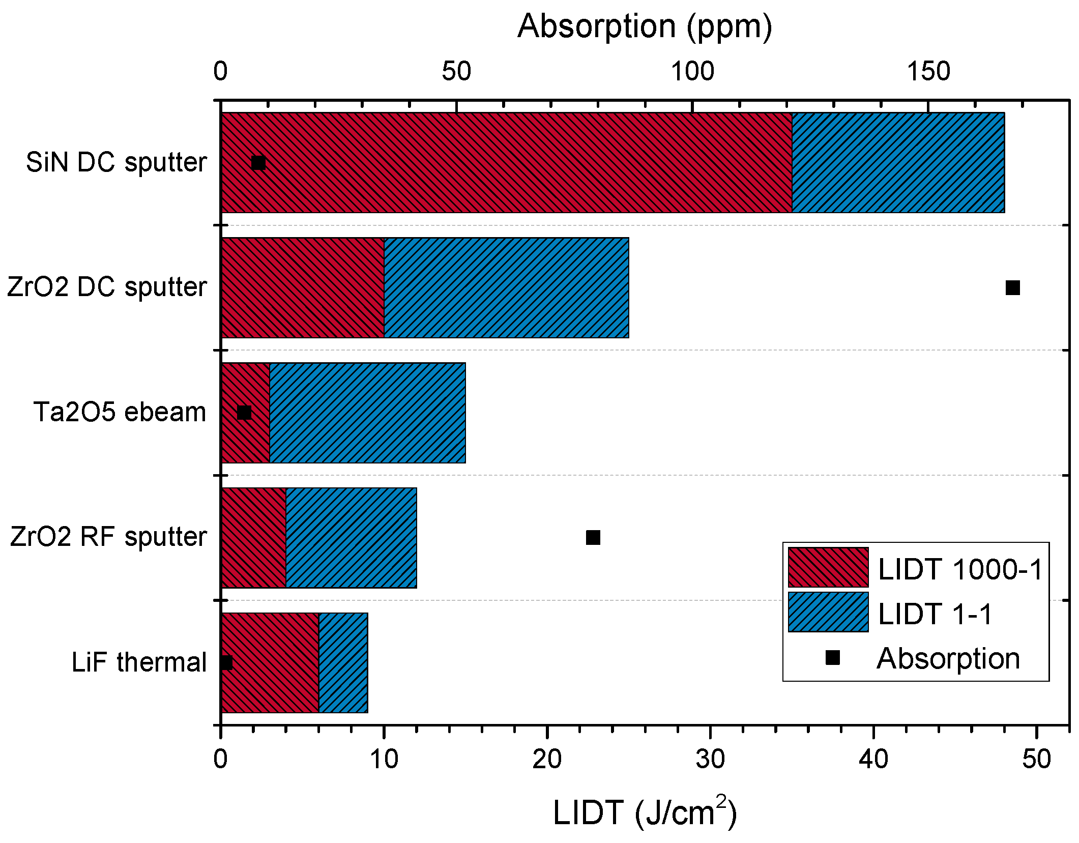
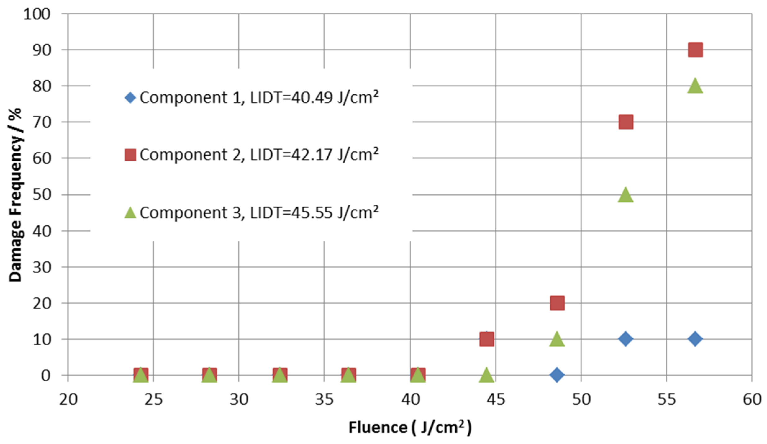
Figure 5,
Figure 6 and
Figure 7 show these LIDT results and demonstrate good agreement between these methods. The strong substrate dependence can be seen when comparing identical coatings grown on witnesses
vs. the finished component (ZrO
2/SiO
2 in
Figure 6,
qv. Figure 7 LIDT values). In
Figure 7, no failures were seen on any of the identical components below 40 J/cm
2. The PCI absorption is also plotted in
Figure 5 and
Figure 6, and, for both the single-layer and AR coatings, there appears to be no direct correlation between the LIDT and coating absorption.
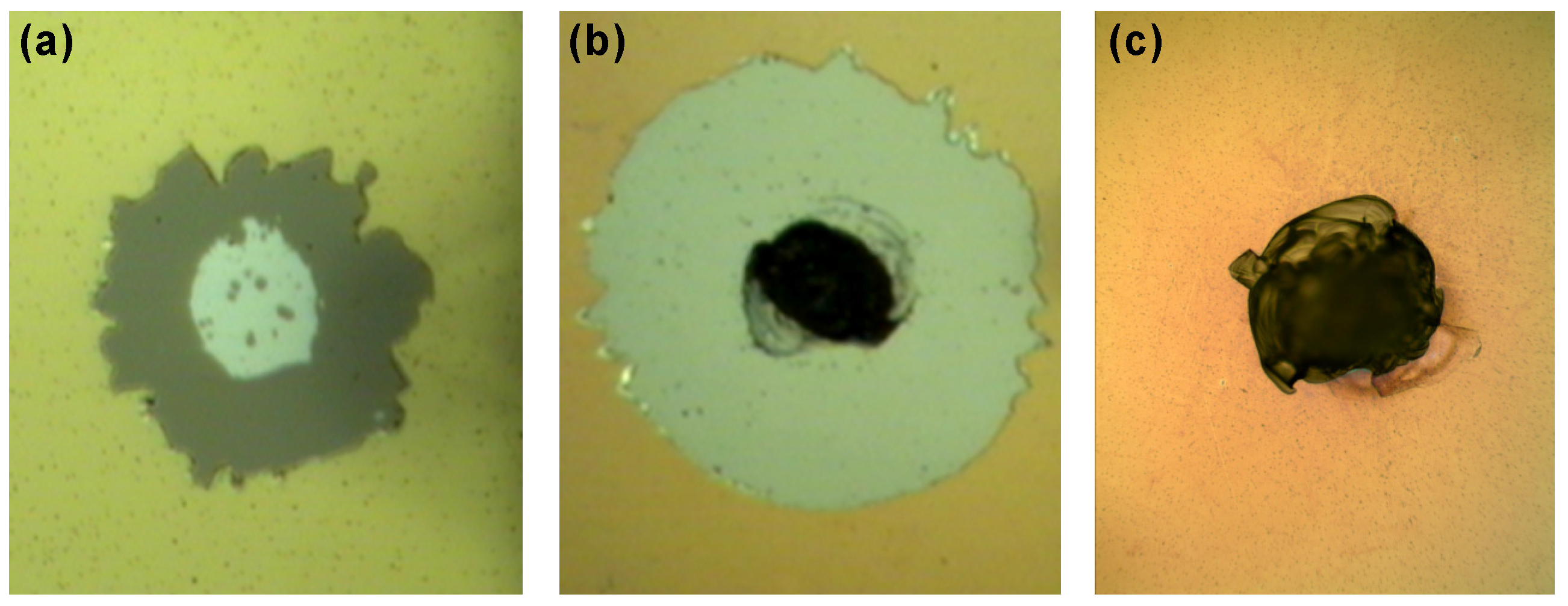
LIDT damage types include material-only ablation (seen in the Nb
2O
5/SiO
2 RF-sputtered coating,
Figure 8a), coating loss, substrate damage (seen in the higher damage-resistant coating such as the ZrO
2/SiO
2 RF-sputtered (
Figure 8b)) and substrate-only damage (seen in the case of the ZrO
2/SiN DC-sputtered coating (
Figure 8c). In some ebeam coating sample cases, thermally induced local damage was also observed.
AFM measurements were also made on a Veeco Dimension V AFM & Nanomechanical Tester. The AFM was set to run in contact mode with a 0.4–0.7 µm-thick non-conductive silicon nitride tip, and is typically able to measure height differences ranging from sub-nanometer to a few microns. Surface roughness, R, of the undamaged coating regions were also measured and gave R = 11.1 ± 0.6 nm for the ZrO2/SiO2 coating and R = 0.85 ± 0.07 nm for the Nb2O5/SiO2 coating.
5. Discussion and Conclusions
The main objective of developing a coating with a LIDT greater than 20 J/cm
2 (1 GW/cm
2) was exceeded comfortably, with double this value being consistently reported. While it has been definitively shown on the final component for only one coating design, it can be demonstrated that other coating material systems have a strong potential and are likely to also meet the requirement. It was also previously reported that a post-deposition annealing at 300 °C consistently reduces absorption as measured by PCI but does not significantly increase the LIDT [
6]. In the case of the ZrO
2/SiO
2 coating, the LIDT is largely limited by the substrate properties: upheld by both substrate PCI absorption measurements and the substrate failure of the top performing samples. There are many possible reasons for this lack of LIDT improvement, including that the baseline absorption is not the dominant mechanism at the measured levels-instead, e.g., electric field breakdown effects may be more prevalent. Similarly, the micro-inclusion content and nanostructure may also be critical, and this could help explain the observed improvement in RF-sputtered materials over their namesakes grown by electron beam evaporation; this can often be seen by surface roughness or by a surface PCI absorption scan.
ZrO
2 appears to have great potential (deposited by either RF or DC sputtering), offering good LIDT performance when used with either SiO
2 or SiN despite also having higher absorption in the latter case. It was expected that the nitride would have a higher damage threshold due to the higher thermal conductivity [
7], which may be the case, but instead it appears limited by the substrate for these samples.
The surface variability in absorption offers deposition technique-related clues that point to the need for higher chamber cleanliness and better control of inclusions (longer source conditioning, better source cleaning, lower deposition rates, longer source-to-substrate separation, etc.), and may also require better substrate cleaning and handling.
From the range of PCI absorption measurements collected for the uncoated substrates (a factor of 400 for seemingly identical transmission by spectrophotometry), an observed enhancement of scratches after laser damage testing on some samples, and an apparent threshold ceiling prior to substrate failure, it would seem prudent to ensure a more standardized starting point for future substrate selection based not only on internal losses but also surface finish, for which such a correlation has long been reported [
8]. Future work would therefore include before-and-after laser damage microscale surface analysis.
It is clear that in some cases the absorption appears to be reduced by the addition of an additional layer. The mechanism is not known but could be due to the prolonged exposure to oxygen plasma, for example, during the second layer or an induced transmission effect or simply variation in the deposition process. Further work is planned to investigate this.
Further investigations planned will explore alternative high index materials including HfO2 and different starting materials for the same final coating chemistry for the reactive ebeam, such as Nb2O5 from Nb metal and SiO2 from Si, to reduce inclusions and scatter centers. It would also be interesting to complete the analysis on single layers such as AlN and ZnSe. A study of the effect of the sputtering rate of ZrO2 on the intrinsic properties and any resultant change in LIDT would also be desirable, given the demonstrated promising performance of the material.

 ,
, 


