Microstructures and Photovoltaic Properties of Zn(Al)O/Cu2O-Based Solar Cells Prepared by Spin-Coating and Electrodeposition

Abstract
:1. Introduction
2. Experimental Procedures
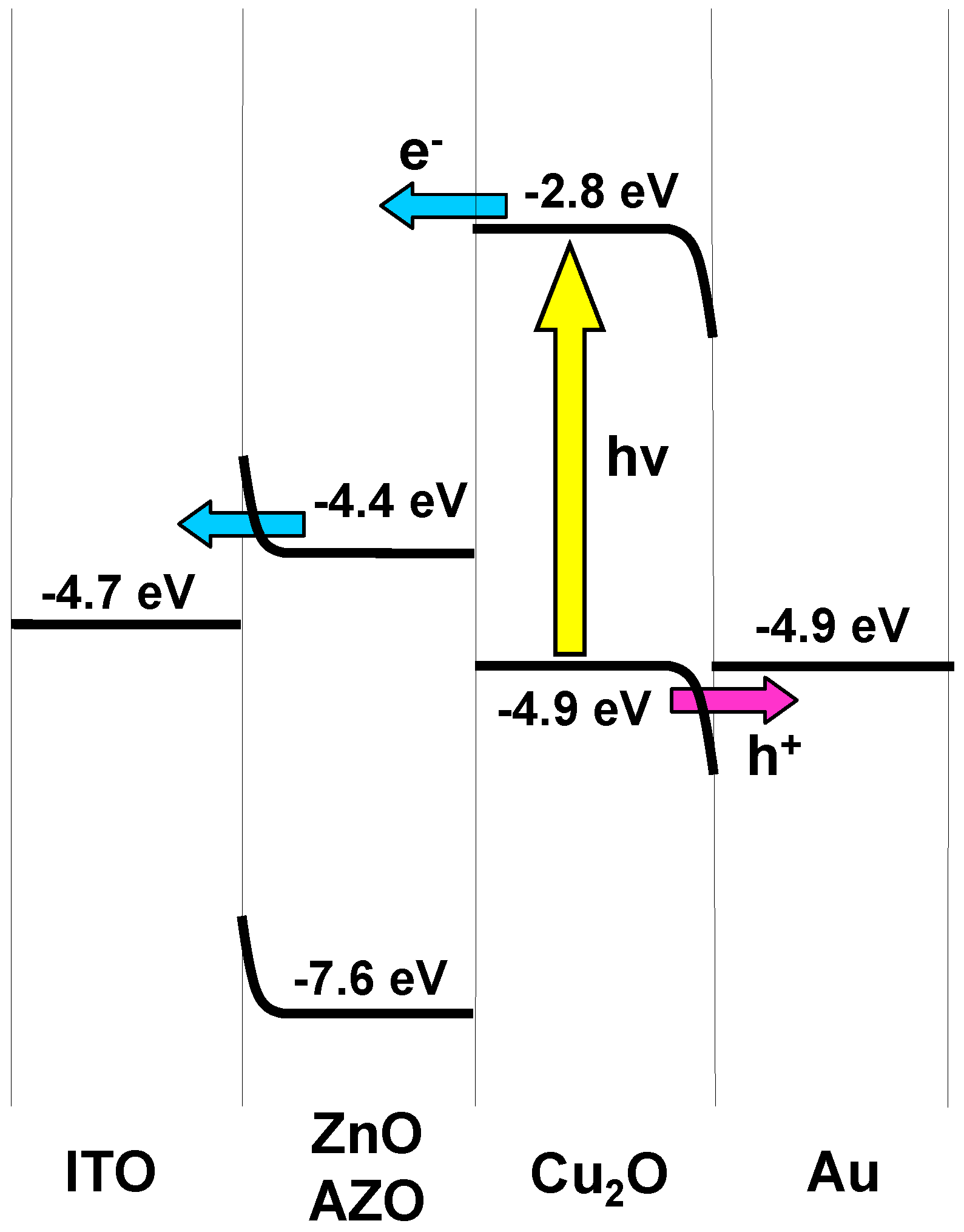
3. Results and Discussion

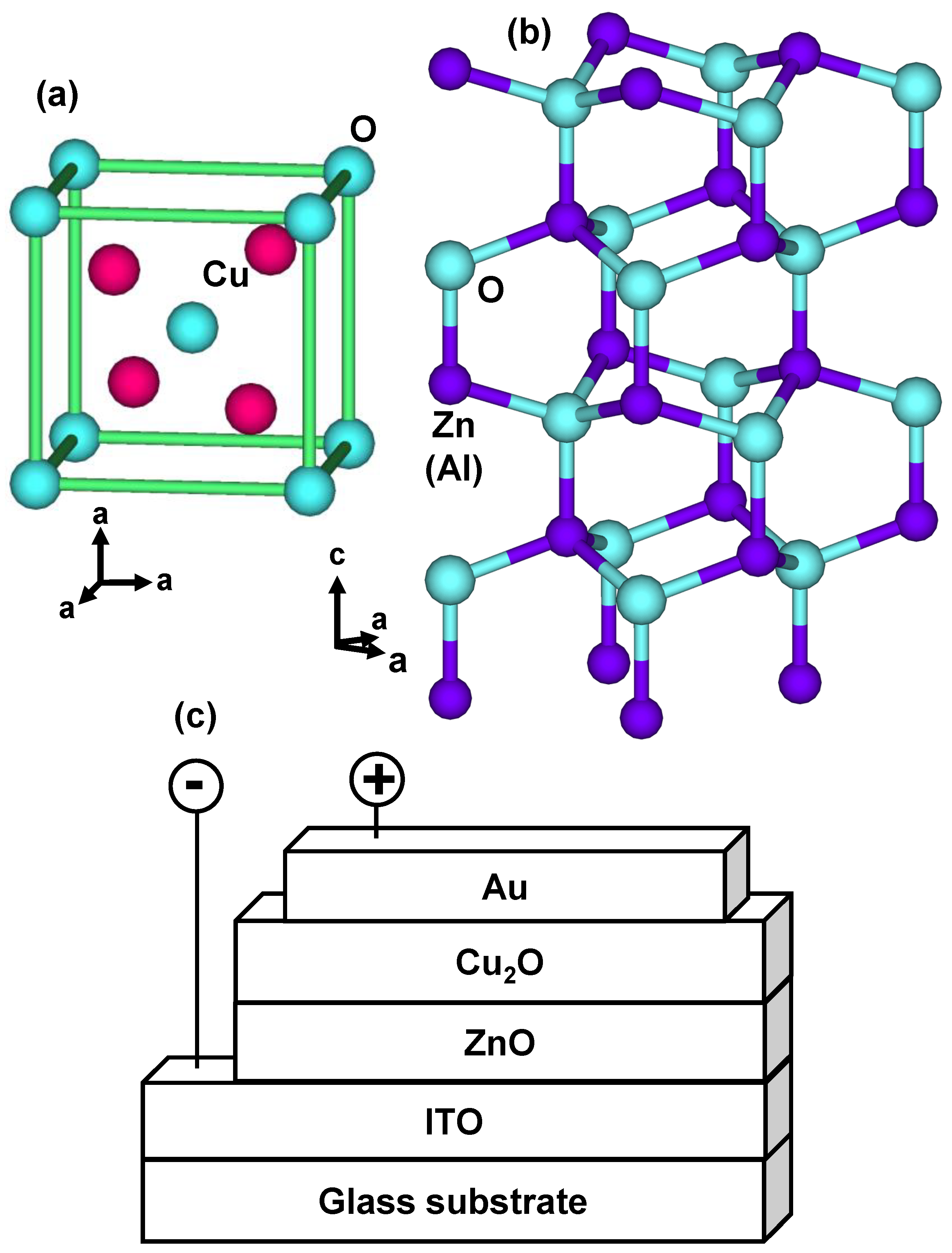
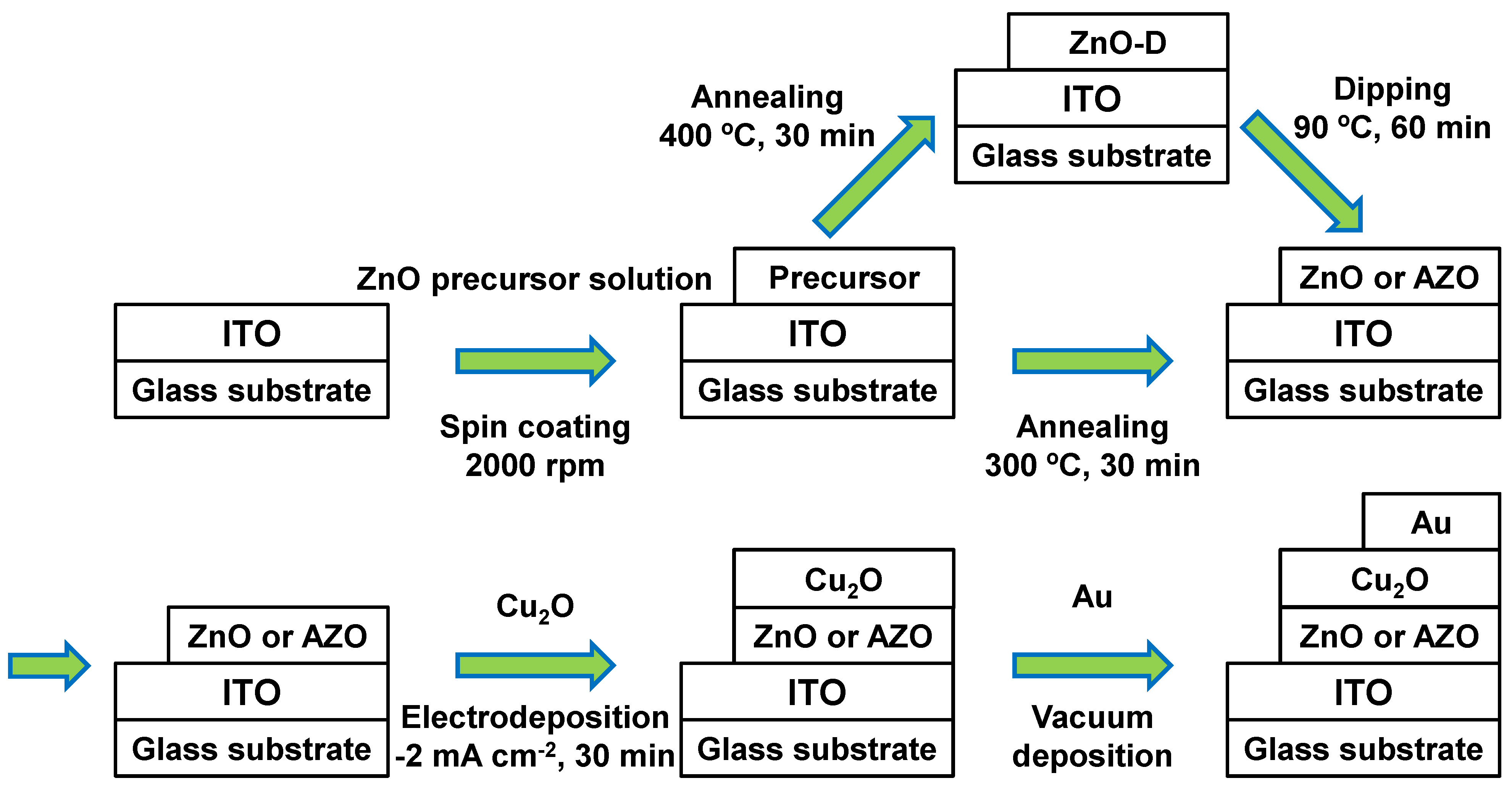
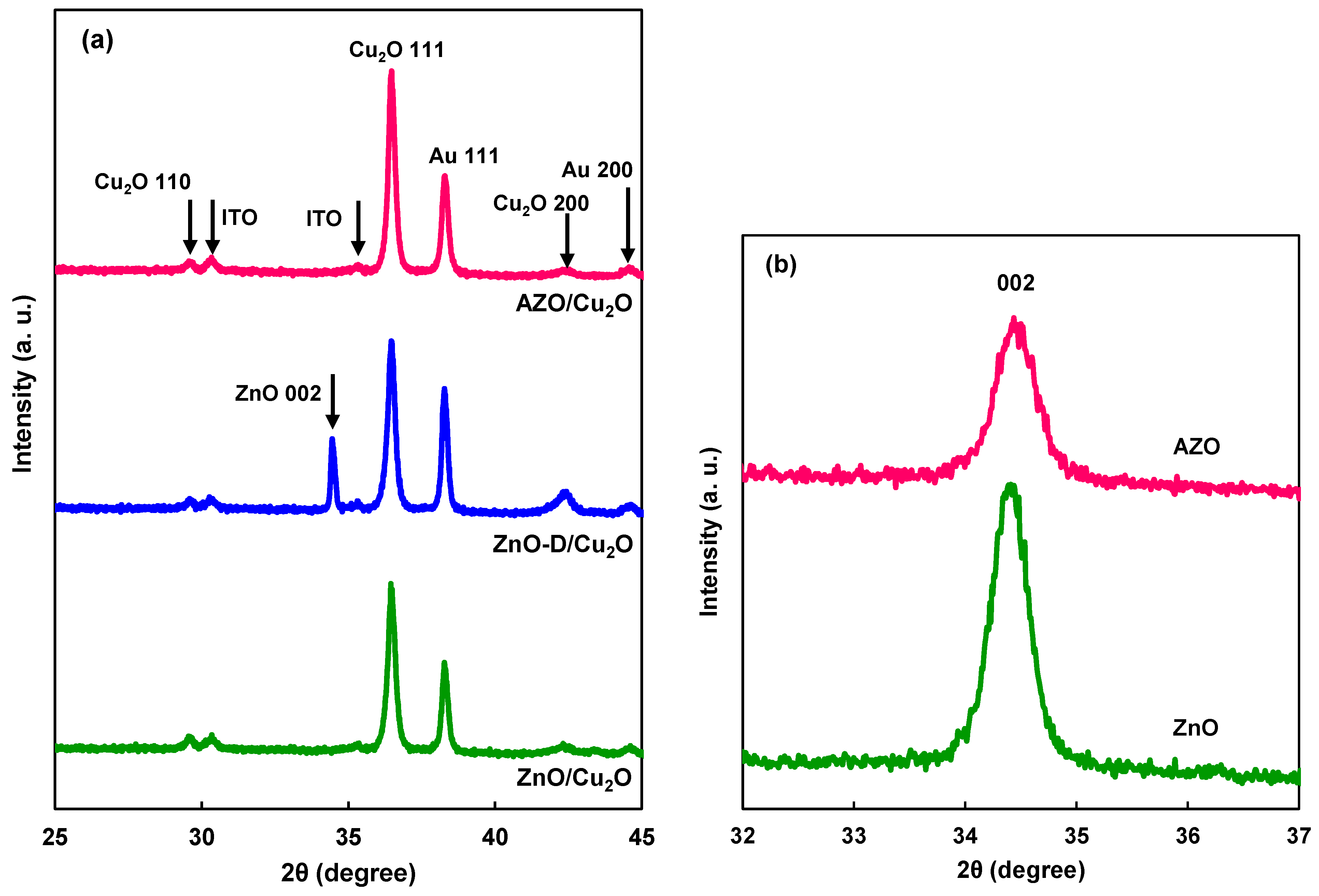
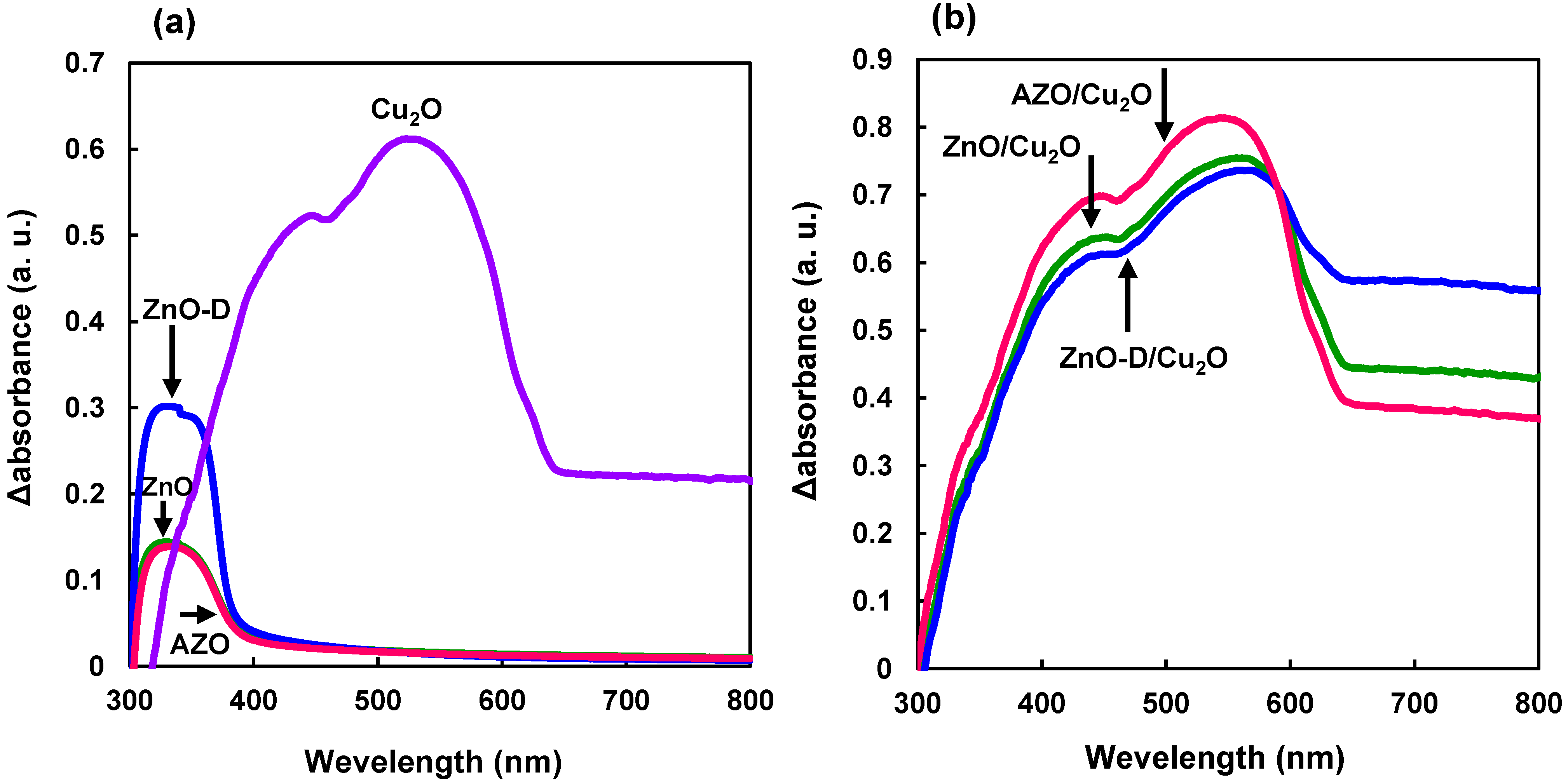
| ZnO formation | Lattice constant c (nm) | Crystallite size (nm) |
|---|---|---|
| ZnO | 0.5211 | 25 |
| ZnO-D | 0.5208 | 104 |
| AZO | 0.5203 | 22 |
| ZnO [24] | 0.52066 | – |
| Cu2O formation | Lattice constant a (nm) | Crystallite size (nm) | I111/I200 |
|---|---|---|---|
| Cu2O on ZnO | 0.4268 | 52 | 19.9 |
| Cu2O on ZnO-D | 0.4268 | 189 | 8.63 |
| Cu2O on AZO | 0.4268 | 86 | 35.7 |
| Cu2O [1] | 0.42696 | – | 2.7 |

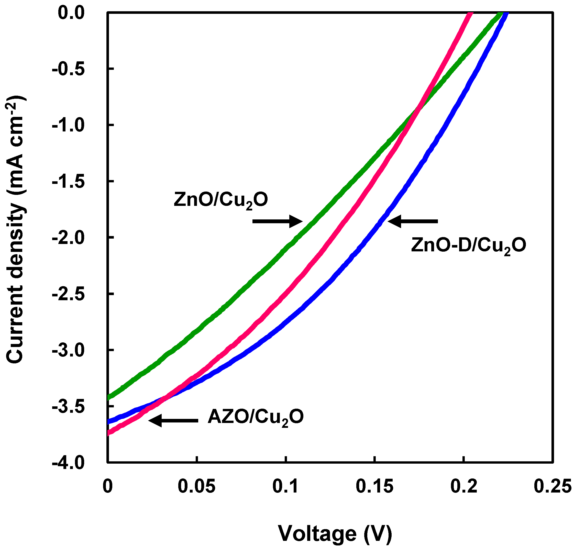
| Devices | JSC (mA·cm−2) | VOC (V) | FF | η (%) | Rs (Ω·cm2) | Rsh (Ω·cm2) |
|---|---|---|---|---|---|---|
| ZnO/Cu2O | 3.4 | 0.22 | 0.29 | 0.22 | 53 | 94 |
| ZnO-D/Cu2O | 3.6 | 0.22 | 0.37 | 0.30 | 32 | 150 |
| AZO/Cu2O | 3.7 | 0.20 | 0.34 | 0.26 | 32 | 100 |

4. Conclusions
Author Contributions
Conflicts of Interest
References
- Swanson, H.E.; Fuyat, R.K. Standard X-ray Diffraction Powder Patterns; U.S. Dept. of Commerce, National Bureau of Standards: Washington, DC, USA, 1953. [Google Scholar]
- Minami, T.; Nishi, Y.; Miyata, T. High-efficiency Cu2O-based heterojunction solar cells fabricated using a Ga2O3 thin film as n-type layer. Appl. Phys. Express 6. [CrossRef]
- Izaki, M.; Shinagawa, T.; Mizuno, K.; Ida, Y.; Inaba, M.; Tasaka, A. Electrochemically constructed p-Cu2O/n-ZnO heterojunction diode for photovoltaic device. J. Phys. D 2007, 40, 3326–3329. [Google Scholar] [CrossRef]
- Duan, Z.; Pasquier, A.D.; Lu, Y.; Xu, Y.; Garfunkel, E. Effects of Mg composition on open circuit voltage of Cu2O–MgxZn1−xO heterojunction solar cells. Sol. Energy Mater. Sol. Cells 2012, 96, 292–297. [Google Scholar] [CrossRef]
- Shao, F.; Sun, J.; Gao, L.; Luo, J.; Liu, Y.; Yang, S. High efficiency semiconductor-liquid junction solar cells based on Cu/Cu2O. Adv. Funct. Mater. 2012, 22, 3907–3913. [Google Scholar] [CrossRef]
- Oku, T.; Takeda, A.; Nagata, A.; Kidowaki, H.; Kumada, K.; Fujimoto, K.; Suzuki, A.; Akiyama, T.; Yamasaki, Y.; Ōsawa, E. Microstructures and photovoltaic properties of C60 based solar cells with copper oxides, CuInS2, phthalocyanines, porphyrin, PVK, nanodiamond, germanium and exciton diffusion blocking layers. Mater. Technol. 2013, 28, 21–39. [Google Scholar]
- Oku, T.; Motoyoshi, R.; Fujimoto, K.; Akiyama, T.; Jeyadevan, B.; Cuya, J. Structures and photovoltaic properties of copper oxides/fullerene solar cells. J. Phys. Chem. Solids 2011, 72, 1206–1211. [Google Scholar] [CrossRef]
- Jeong, S.S.; Mittiga, A.; Salza, E.; Masci, A.; Passerini, S. Electrodeposited ZnO/Cu2O heterojunction solar cells. Electrochim. Acta 2008, 53, 2226–2231. [Google Scholar] [CrossRef]
- Izaki, M.; Mizuno, K.; Shinagawa, T.; Inaba, M.; Tasaka, A. Photochemical construction of photovoltaic device composed of p-Copper(I) Oxide and n-Zinc Oxide. J. Electrochem. Soc. 2006, 153, C668–C672. [Google Scholar] [CrossRef]
- Anandan, S.; Wen, X.; Yang, S. Room temperature growth of CuO nanorod arrays on copper and their application as a cathode in dye-sensitized solar cells. Mater. Chem. Phys. 2005, 93, 35–40. [Google Scholar] [CrossRef]
- Cui, J.; Gibson, U.J. A simple two-step electrodeposition of Cu2O/ZnO nanopillar solar cells. J. Phys. Chem. C 2010, 114, 6408–6412. [Google Scholar]
- McShane, C.M.; Choi, K.-S. Junction studies on electrochemically fabricated p-n Cu2O homojunction solar cells for efficiency enhancement. Phys. Chem. Chem. Phys. 2012, 14, 6112–6118. [Google Scholar] [CrossRef]
- Nakaoka, K.; Ueyama, J.; Ogura, K. Photoelectrochemical behavior of electrodeposited CuO and Cu2O thin films on conducting substrates. J. Electrochem. Soc. 2004, 151, C661–C665. [Google Scholar] [CrossRef]
- Leopold, S.; Herranen, M.; Carlsson, J.-O. Spontaneous potential oscillations in the Cu(II)/Tartrate and lactate systems, aspects of mechanisms and film deposition. J. Electrochem. Soc. 2001, 148, C513–C517. [Google Scholar] [CrossRef]
- Izaki, M.; Omi, T. Electrolyte optimization for cathodic growth of zinc oxide films. J. Electrochem. Soc. 1996, 143, L53–L55. [Google Scholar] [CrossRef]
- Golden, T.D.; Shumsky, M.G.; Zhou, Y.; VanderWerf, R.A.; Van Leeuwen, R.A.; Switzer, J.A. Electrochemical deposition of copper(I) oxide films. Chem. Mater. 1996, 8, 2499–2504. [Google Scholar] [CrossRef]
- Mizuno, K.; Izaki, M.; Murase, K.; Shinagawa, T.; Chigane, M.; Inaba, M.; Tasaka, A.; Awakura, Y. Structural and electrical characterizations of electrodeposited p-type semiconductor Cu2O films. J. Electrochem. Soc. 2005, 152, C179–C182. [Google Scholar] [CrossRef]
- Mahalingam, T.; John, V.S.; Hsu, L.S. Microstructural analysis of electrodeposited zinc oxide thin films. J. New Mater. Electrochem. Syst. 2007, 10, 9–14. [Google Scholar]
- Georgieva, V.; Ristov, M. Electrodeposited cuprous oxide on indium tin oxide for solar applications. Sol. Energy Mater. Sol. Cells 2002, 73, 67–73. [Google Scholar] [CrossRef]
- Caballero-Briones, F.; Artés, J.M.; Díez-Pérez, I.; Gorostiza, P.; Sanz, F. Direct observation of the valence band edge by in situ ECSTM-ECTS in p-type Cu2O layers prepared by copper anodization. J. Phys. Chem. C 2009, 113, 1028–1036. [Google Scholar] [CrossRef]
- Chu, C.W.; Shrotriya, V.; Li, G.; Yang, Y. Tuning acceptor energy level for efficient charge collection in copper-phthalocyanine-based organic solar cells. Appl. Phys. Lett. 2006, 88. [Google Scholar] [CrossRef]
- Green, M.A.; Emery, K.; King, D.L.; Hishikawa, Y.; Warta, W. Solar cell efficiency tables (version 28). Prog. Photovolt. 2006, 14, 455–461. [Google Scholar] [CrossRef]
- Fujimoto, K.; Oku, T.; Akiyama, T. Fabrication and characterization of ZnO/Cu2O solar cells prepared by electrodeposition. Appl. Phys. Express 2013, 6. [Google Scholar] [CrossRef]
- McMurdie, H.; Morris, M.; Evans, E.; Paretzkin, B.; Wong-Ng, W.; Ettlinger, L.; Hubbard, C. Standard X-ray diffraction powder patterns from the JCPDS research associateship. Powder Diffr. 1986, 1, 64–77. [Google Scholar] [CrossRef]
- Minami, T.; Miyata, T.; Ihara, K.; Minamino, Y.; Tsukada, S. Effect of ZnO film deposition methods on the photovoltaic properties of ZnO–Cu2O heterojunction devices. Thin Solid Films 2006, 494, 47–52. [Google Scholar] [CrossRef]
- Wei, H.; Gong, H.; Wang, Y.; Hu, X.; Chen, L.; Xu, H.; Liub, P.; Cao, B. Three kinds of Cu2O/ZnO heterostructure solar cells fabricated with electrochemical deposition and their structure-related photovoltaic properties. CrystEngComm 2011, 13, 6065–6070. [Google Scholar] [CrossRef]
- Fujimoto, K.; Oku, T.; Akiyama, T.; Suzuki, A. Fabrication and characterization of copper oxide-zinc oxide solar cells prepared by electrodeposition. J. Phys. Conf. Ser. 2013, 433. [Google Scholar] [CrossRef]
- Mittiga, A.; Salza, E.; Sarto, F.; Tucci, M.; Vasanthi, R. Heterojunction solar cell with 2% efficiency based on a Cu2O substrate. Appl. Phys. Lett. 2006, 88. [Google Scholar] [CrossRef]
- Raksa, P.; Nilphai, S.; Gardchareon, A.; Choopun, S. Copper oxide thin film and nanowire as a barrier in ZnO dye-sensitized solar cells. Thin Solid Films 2009, 517, 4741–4744. [Google Scholar] [CrossRef]
- Minami, T.; Nishi, Y.; Miyata, T.; Nomoto, J. High-efficiency oxide solar cells with ZnO/Cu2O heterojunction fabricated on thermally oxidized Cu2O sheets. Appl. Phys. Express 2011, 4. [Google Scholar] [CrossRef]
- Minami, T.; Tanaka, H.; Shimakawa, T.; Miyata, T.; Sato, H. High-efficiency oxide heterojunction solar cells using Cu2O sheets. Jpn. J. Appl. Phys. 2004, 43, L917–L919. [Google Scholar] [CrossRef]
- Fan, X.; Fang, G.; Guo, S.; Liu, N.; Gao, H.; Qin, P.; Li, S.; Long, H.; Zheng, Q.; Zhao, X. Controllable synthesis of flake-like Al-doped ZnO nanostructures and its application in inverted organic solar cells. Nanoscale Res. Lett. 2011, 6, 546:1–546:6. [Google Scholar]
- Septina, W.; Ikeda, S.; Khan, M.A.; Hirai, T.; Harada, T.; Matsumura, M.; Peter, L.M. Potentiostatic electrodeposition of cuprous oxide thin films for photovoltaic applications. Electrochim. Acta 2011, 56, 4882–4888. [Google Scholar] [CrossRef]
- Kang, D.W.; Kuk, S.H.; Ji, K.S.; Lee, H.M.; Han, M.K. Effects of ITO precursor thickness on transparent conductive Al doped ZnO film for solar cell applications. Sol. Energy Mater. Sol. Cells 2011, 95, 138–141. [Google Scholar] [CrossRef]
- Minami, T.; Nishi, Y.; Miyata, T.; Abe, S. Photovoltaic properties in Al-doped ZnO/non-doped Zn1−xMgxO/Cu2O heterojunction solar cells. ECS Trans. 2013, 50, 59–68. [Google Scholar] [CrossRef]
- Liu, Y.; Turley, H.K.; Tumbleston, J.R.; Samulski, E.T.; Lopez, R. Minority carrier transport length of electrodeposited in heterojunction solar cells. Appl. Phys. Lett. 2011, 98. [Google Scholar] [CrossRef]
- Musselman, K.P.; Wisnet, A.; Iza, D.C.; Hesse, H.C.; Scheu, C.; MacManus-Driscoll, J.L.; Schmidt-Mende, L. Strong efficiency improvements in ultra-low-cost inorganic nanowire solar cells. Adv. Mater. 2010, 22, E254–E258. [Google Scholar] [CrossRef]
- Yi, S.H.; Choi, S.K.; Jang, J.M.; Kim, J.A.; Jung, W.G. Properties of aluminum doped zinc oxide thin film by sol-gel process. Proc. SPIE 2008, 6831. [Google Scholar] [CrossRef]
- Xu, T.; Venkatesan, S.; Galipeau, D.; Qiao, Q. Study of polymer/ZnO nanostructure interfaces by Kelvin probe force microscopy. Sol. Energy Mater. Sol. Cells 2013, 108, 246–251. [Google Scholar] [CrossRef]
- Marin, A.T.; Muñoz-Rojas, D.; Iza, D.C.; Gershon, T.; Musselman, K.P.; MacManus-Driscoll, J.L. Novel atmospheric growth technique to improve both light absorption and charge collection in ZnO/Cu2O thin film solar cells. Adv. Funct. Mater. 2013, 23, 3413–3419. [Google Scholar] [CrossRef]
© 2014 by the authors; licensee MDPI, Basel, Switzerland. This article is an open access article distributed under the terms and conditions of the Creative Commons Attribution license (http://creativecommons.org/licenses/by/3.0/).
Share and Cite
Oku, T.; Yamada, T.; Fujimoto, K.; Akiyama, T. Microstructures and Photovoltaic Properties of Zn(Al)O/Cu2O-Based Solar Cells Prepared by Spin-Coating and Electrodeposition. Coatings 2014, 4, 203-213. https://doi.org/10.3390/coatings4020203
Oku T, Yamada T, Fujimoto K, Akiyama T. Microstructures and Photovoltaic Properties of Zn(Al)O/Cu2O-Based Solar Cells Prepared by Spin-Coating and Electrodeposition. Coatings. 2014; 4(2):203-213. https://doi.org/10.3390/coatings4020203
Chicago/Turabian StyleOku, Takeo, Tetsuya Yamada, Kazuya Fujimoto, and Tsuyoshi Akiyama. 2014. "Microstructures and Photovoltaic Properties of Zn(Al)O/Cu2O-Based Solar Cells Prepared by Spin-Coating and Electrodeposition" Coatings 4, no. 2: 203-213. https://doi.org/10.3390/coatings4020203