Article

A Bilayer 2D-WS2/Organic-Based Heterojunction for High-Performance Photodetectors

1
College of Materials & Environmental Engineering, Hangzhou Dianzi University, Hangzhou 310018, China
2
Tsinghua-Berkeley Shenzhen Institute (TBSI), Tsinghua University, Shenzhen 518055, China
3
Tsinghua Shenzhen International Graduate School, Tsinghua University, Shenzhen 518000, China
4
Department of Mechanical Engineering, The University of Hong Kong, Pokfulam, Hong Kong, China
5
Institute of Electro-Optical Engineering, National Chiao Tung University, Hsinchu 30010, Taiwan
6
Department of Electrical Engineering and Computer Sciences and Tsinghua-Berkeley Shenzhen Institute (TBSI), University of California at Berkeley, Berkeley, CA 94720, USA
*
Authors to whom correspondence should be addressed.
These authors contributed equally to this work.
Nanomaterials 2019, 9(9), 1312; https://doi.org/10.3390/nano9091312
Submission received: 16 August 2019 / Revised: 9 September 2019 / Accepted: 10 September 2019 / Published: 13 September 2019
(This article belongs to the Special Issue Quantum Dots and Micro-LED Display)

Abstract

:
Two-dimensional (2D) tungsten disulfide (WS2) has inspired great efforts in optoelectronics, such as in solar cells, light-emitting diodes, and photodetectors. However, chemical vapor deposition (CVD) grown 2D WS2 domains with the coexistence of a discontinuous single layer and multilayers are still not suitable for the fabrication of photodetectors on a large scale. An emerging field in the integration of organic materials with 2D materials offers the advantages of molecular diversity and flexibility to provide an exciting aspect on high-performance device applications. Herein, we fabricated a photodetector based on a 2D-WS2/organic semiconductor materials (mixture of the (Poly-(N,N′-bis-4-butylphenyl-N,N′-bisphenyl) benzidine and Phenyl-C61-butyric acid methyl ester (Poly-TPD/PCBM)) heterojunction. The application of Poly-TPD/PCBM organic blend film enhanced light absorption, electrically connected the isolated WS2 domains, and promoted the separation of electron-hole pairs. The generated exciton could sufficiently diffuse to the interface of the WS2 and the organic blend layers for efficient charge separation, where Poly-TPD was favorable for hole carrier transport and PCBM for electron transport to their respective electrodes. We show that the photodetector exhibited high responsivity, detectivity, and an on/off ratio of 0.1 A/W, 1.1 × 10¹¹ Jones, and 100, respectively. In addition, the photodetector showed a broad spectral response from 500 nm to 750 nm, with a peak external quantum efficiency (EQE) of 8%. Our work offers a facile solution-coating process combined with a CVD technique to prepare an inorganic/organic heterojunction photodetector with high performance on silicon substrate.

1. Introduction

Two-dimensional materials (2D), such as graphene, hexagonal boron nitride, transition metal dichalcogenides, tin sulfide, black phosphorus, ultrasmall bismuth quantum dots, and selenium nanoflakes, have become optically active semiconductors in biomedicine, ion detectors, and photodetectors (PDs). Photodetector-based graphene exhibits a large-response wavelength range and a high on/off ratio. Two-dimensional black phosphorus, with an anisotropic band structure, shows linear dichroism and anisotropic absorption. Photodetector-based monolayer black phosphorus exhibits excellent polarization sensitivity with a large bandwidth. Photoelectric properties of transition metal dichalcogenides (TMDs) have a remarkable change, as bulk transforms into a monolayer or multilayers, which have high optical absorption rates and suitable band gaps. Photodetector-based monolayer transition metal dichalcogenides (TMDs) show high quantum efficiency and low response times [1,2,3,4,5,6,7,8,9,10,11,12]. Among these 2D materials, tungsten disulfide (WS2) layers with high mobility of 1000 cm2·v−1·s−1, a high optical absorption coefficient of ca. 106 cm−1, and a band gap of 1.9 eV [13,14,15,16] are typical n-type 2D materials for electronic and optoelectronic device applications, making them compatible to combine with other materials to construct 2D van der Waals heterostructures.
Organic materials are suitable materials to vertically stack together with 2D WS2 layers to form an energy-favorable inorganic/organic heterojunction, providing an effective interface to separate the electron-hole (e-h) pairs excited by incident photons. A significant advantage to employing organic materials is due to their facile solution processability [17,18,19,20,21,22]. Nowadays, it remains challenging to form uniform 2D WS2 thin films on a large scale due to the coexistence of discontinuous and isolated single layers and multilayers [23,24,25,26,27]. Due to the excellent flexibility of organic materials, the surface of the isolated 2D WS2 layers could be effectively smoothed out and interconnected together, filling pinholes and vacancies of the 2D layers underneath. Recently, research has been intensively carried out to combine 2D inorganic materials with organic materials to form energy-favorable junctions for efficient exciton dissociation and charge transport [28,29,30,31,32,33,34]. Two-dimensional CsPbBr3 nanosheets have been assembled into flexible heterojunction films with phenyl-C61-butyric acid methyl ester (PCBM), and the 2D CsPbBr3/PCBM photodetectors exhibited an enhanced responsivity of 10.85 AW−1 and an ultrahigh detectivity of 3.0 × 10¹³ Jones [30]. The van der Waals heterojunction formed between pentacene and 2D MoS2 has demonstrated an ultrafast charge transfer of 6.7 ps (especially the charge-separated state that lives for 5.1 ns) up to an order of magnitude longer than the pure 2D heterojunctions, suggesting the benefits of junction-stacking organic/2D materials [31]. Therefore, an emerging field in the integration of organic materials with 2D materials provides an exciting aspect on continuous 2D device fabrication. A hole transport material, Poly-(N,N′-bis-4-butylphenyl-N,N′-bisphenyl) benzidine (Poly-TPD), and an electron transport material, PCBM, are often used for hole and electron transporting layers in organic photodetectors and solar cells [35,36,37]. Two-dimensional WS2 (conductive band edge at ca. −3.84 eV and valence band edge at ca. −5.82 eV for a monolayer) is a perfect match for the Poly-TPD/PCBM mixture (LUMO at −4.1 eV of PCBM to accept electrons and HOMO at −5.2 eV of Poly-TPD to accept holes), which is favorable for exciton dissociation [38,39,40,41,42,43].
The growth of monolayer WS2 is always a big challenge, especially for the large-scale monolayer WS2. Herein, the large-scale monolayer WS2 was successfully prepared using ZnO film as an auxiliary material on an SiO2/Si substrate through chemical vapor deposition (CVD) for the first time. With a convenient solution spin-coating technique, the blend film of mixed Poly-TPD and PCBM at a weight ratio of 1:1 was deposited on top of the 2D WS2 to form an ordered bilayer inorganic/organic diode. The 2D WS2 thin films, obtained from ZnO-controlled growth through chemical vapor deposition (CVD), provided inert and solid surfaces. The van der Waals force interactions of 2D WS2 and organic layers could allow for the planar growth of organic-based films with larger crystal grain sizes. In the meantime, organic layers could smooth out the surface of the 2D WS2 layer for continuous device fabrication, which could substantially suppress dark currents. Thus, functionalized organic thin films and suitable architectures with 2D WS2 must be well optimized in order to realize inorganic/organic-based PDs with high performance.
Overall, the 2D WS2/Poly-TPD/PCBM PD obtained a broad spectral response from 500 nm to 750 nm with a peak external quantum efficiency (EQE) of 8% at a wavelength of 527 nm. When illuminated with a 450-nm excitation laser at a power intensity of 0.14 mW/cm2, the PD showed a gate-tunable responsivity, a specific detectivity (D*), and an on/off ratio of 0.1 A/W, 1.1 × 10¹¹ Jones, and 100, respectively. Meanwhile, the responsivity dramatically increased with the laser excitation intensity, then saturated to 17 A/W when the drain voltage VD was 10 V. As a result, the 2D inorganic/organic bilayer heterojunction was successfully demonstrated for a high-performance PD and could extend to other organics and 2D materials.

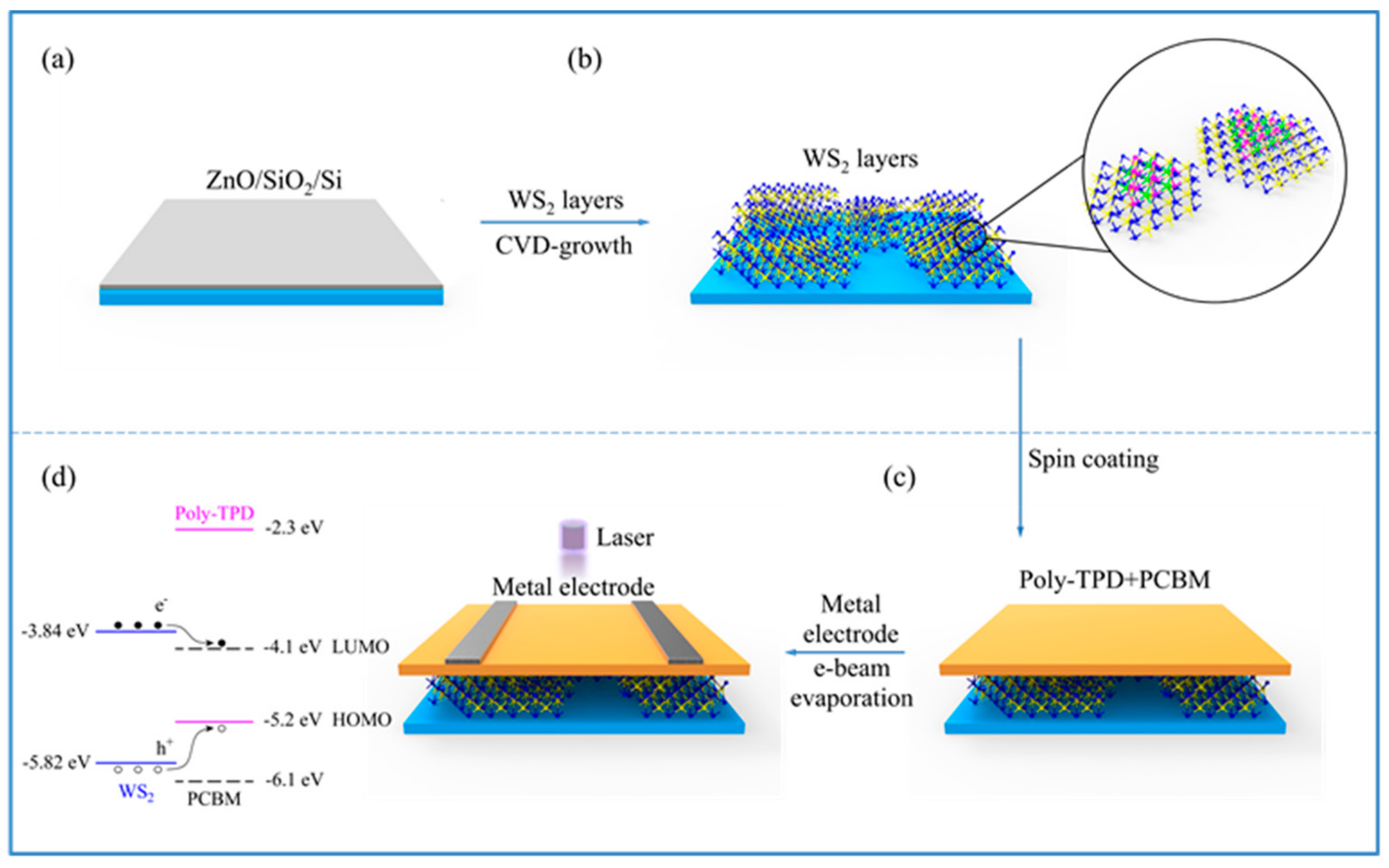
2. Materials and Methods

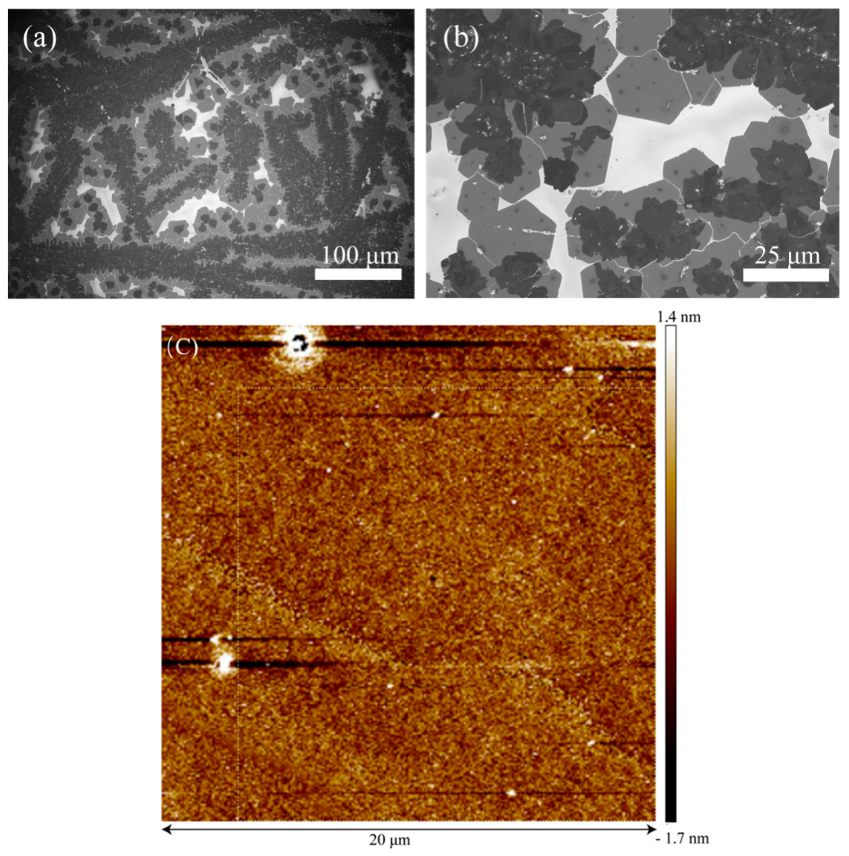
Fabrication and Characterizations

ZnO film was prepared on an SiO2/Si substrate at a thickness of ca. 100 nm through DC reactive magnetron sputtering (Figure 1a) [44]. Metal zinc (DingWei, Dongguan, China) was used as a target. Argon (Ar) was used as the sputtering gas and oxygen as the reactant. Ar/O2 (Ar 20 sccm, O2 60 sccm, 0.3 Pa) was introduced into the sputtering chamber. A negative bias voltage of −300 V was applied to keep glow discharge for 30 min. WS2 film was prepared through a CVD method (Figure 1b) [45,46]. The WS2 powders (Aladdin, Shanghai, China) were loaded in the center of the CVD system and heated to 1000 °C from room temperature over 30 min. An SiO2/Si substrate with a layer of ZnO (ZnO/SiO2/Si) was placed in the downstream region of the CVD. During the above process, the substrate was heated to ca. 700 °C, which was kept for 60 min. Ar/H2 (H2 5%, 105 Pa, 35 sccm) was used as a carrier gas [47]. The spin-coating method was applied to prepare the Poly-TPD/PCBM (1:1) thin film on the top of the WS2 thin film (Figure 1c). The Poly-TPD (Aladdin, Shanghai, China) and PCBM (Aladdin, Shanghai, China) were first dissolved in chlorobenzene solvent with a mass concentration of 10 mg/mL. The spin-casting processes were performed in a glove box. The blend layer of organic materials was spin-coated at 3000 rpm for 50 s, followed by annealing at 110 °C for 30 min. Cr–Au electrodes were e-beam-evaporated on top of organic thin films through a shadow mask with an exposed active area under a vacuum of 1.3 × 10⁻³ Pa (Figure 1d). Here, the channel width of the device was 20 μm, and the length was 100 μm. The final structure of the typical device, on top of an oxidized silicon wafer, was Au/Poly-TPD/PCBM/WS2/Au. The doped silicon could be used as a back gate and SiO2 as a gate dielectric. A schematic diagram of the prepared 2D WS2/organic photodetector with the respective energy level alignments is shown in Figure 1d.
X-ray diffraction (XRD) was performed on a Thermo ARLXTRA (Geneva, Switzerland). X-ray photoelectron spectroscopy (XPS) spectra were performed on an Ulvac-Phi PHI5000 Versaprobe II (Kanagawa, Japan). UV-Vis absorption was performed on a Shimadzu UV-3600 (Kyoto, Japan). Field emission scanning electron microscopy (FESEM) was performed on a FEI Apreo S HiVac (Hillsboro, OR, USA). Raman spectra and photoluminescence (PL) were performed on a micro-Raman setup consisting of a 532-nm solid state laser, a Nikon inverted microscope (Ti eclipse, Tokyo, Japan), a long-pass edge filter (Semrock, New York, NY, USA), and a Raman spectrometer (Horiba, iHR320, Kyoto, Japan). An optical microscope image and a luminescence image were taken on a Jiangnan MV 3000 digital microscope (Nanjing, China). An electrical measurement was carried out on an Agilent 4200 SCS (CA, America) and a LakeShore TTPX (Columbus, OH, USA). The photodetection properties were examined with laser excitation wavelengths of 450 nm to 750 nm.

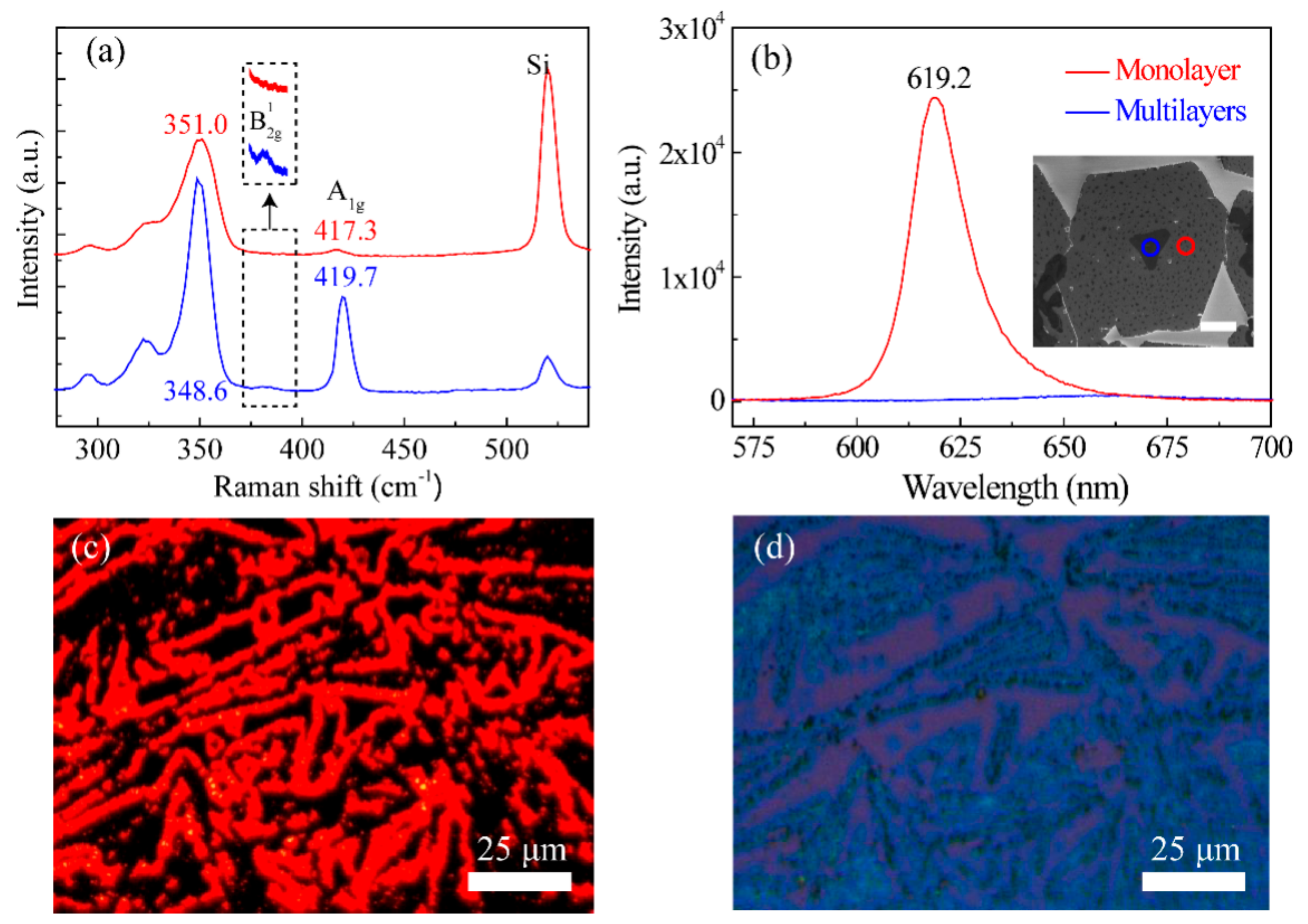
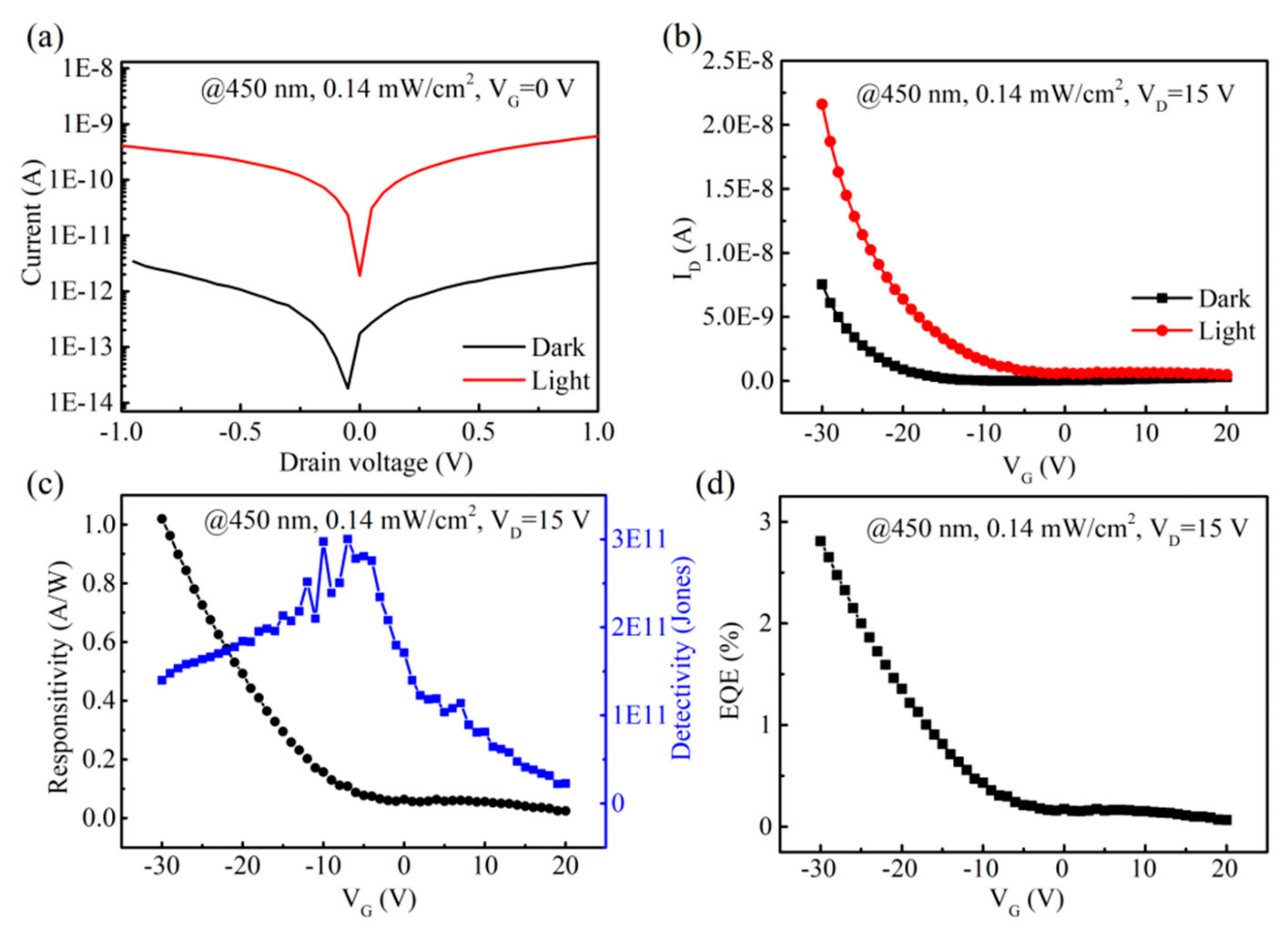
3. Results and Discussion

Figure 2a shows the XRD spectra of the ZnO/SiO2/Si substrate before and after the growth of the WS2 film. The XRD data reveal that WS2 film along with (002) direction was prepared on the Si substrate [48]. The full width at half maximum (FWHM) of the WS2 XRD peak (002) was similar to that of the Si single crystal, indicating that a WS2 film with a single crystalline with a large crystal grain size was obtained. There was no ZnO XRD peak that existed after complete 2D WS2 growth (Figure 2a) [34], which was further confirmed by the XPS spectrum, since no Zn2+ signal (Zn 2P1/2 at 1021.75 eV and Zn 2P3/2 at 1044.7 eV) was detected (see Figure 2b) [49]. The detailed mechanism of 2D WS2 controlled growth was discussed in our previous work [50]. The shape and scale of the monolayer WS2 was affected by the atomic ratio of W/S. When the atomic ratio of W/S was less or larger than 1:2, the monolayer WS2 would only grow into a small triangular shape. Therefore, it was critical to maintain the atomic ratio of W/S to as close to 1:2 as possible. Since ZnO whiskers can absorb extra W atoms to form a ZnWO4 compound in a way that adjusts the atomic ratio of W/S back to 1:2, the WS2 could be promoted further to grow into large-scale monolayer domains. We speculated the ZnWO4 was sublimated and removed from the substrate during the subsequent growth stage.
The UV-Vis absorption spectrum of the WS2 film is shown in Figure 2c. The A peak (located at 575–670 nm) and B peak (located at 527.7 nm) were due to the A and B exciton absorptions, respectively [51,52]. Due to spin-orbit coupling, the valence band split into two sub-bands (v1 and v2, v1 < v2) at the K point of the Brillouin zone. Transitions from v1 and v2 to the minimum of the conduction band corresponded to the B exciton and A exciton, respectively [53]. The A peak consisted of two peaks at 584.1 nm (A(X)) and 626.3 nm (A(X)). A(X) was due to the neutral exciton absorption, and A(X) was due to the charged exciton absorption [54]. In addition, there was a broad peak I at the low-energy side of the A peak (>700 nm). The weak and broad peak I was ascribed to the indirect band gap transition of the multilayers/bulk [24]. Figure 2d shows the absorption spectrum of the organic Poly-TPD/PCBM (1:1) thin films, with two strong absorption peaks in the near-UV region (300–420 nm).
Figure 3 shows typical FESEM images of WS2 film grown on the silicon substrate via the CVD method. The white-colored area in Figure 3a,b is the SiO2/Si substrate. The gray-colored areas with the hexagonal shape are WS2 monolayers. The hexagon morphology indicated that the WS2 monolayer we prepared had a single crystalline with a large crystal grain size. The dark-colored areas with irregular morphology were due to the WS2 multilayers. The small-sized multilayers were stacked on a monolayer with a large domain size. During WS2 growth, hexagonal WS2 monolayers merged together. As shown in Figure 3b, cracks in these hexagonal interfaces could be clearly viewed, and they could have formed during the CVD growth or cooling process. For the Poly-TPD/PCBM (1:1) blend films, the roughness was 0.5 nm in Figure 3c, indicating that Poly-TPD and PCBM were uniformly mixed together, which was required for the subsequent Au electrode deposition. If the surface of the organic blend film were not smooth, the deposited Au atoms could penetrate through the vacancies or voids of the 2D WS2 materials, and the as-prepared devices would be very leaky. Therefore, the uniform feature of the blend film was crucial to a successful 2D WS2/organic photodetector fabrication.
Typical Raman spectra of the WS2 films at room temperature with a 532-nm laser excitation are shown in Figure 4a. The red and blue curves in Figure 4a approximately correspond to the areas circled with a red line and blue line in the inset of Figure 4b, respectively. The Raman peak of silicon (Si) at 520 cm−1 was used to calibrate the Raman spectra of the as-prepared WS2 thin films. Two typical Raman peaks at 351 cm−1 (E2g1) and 417.3 cm−1 (A1g) were observed in the red curve [55]. The frequency difference between the two modes was 66.3 cm−1. The peak intensity ratio of A1g/E2g1 was 0.029. The narrow frequency difference, small peak intensity ratio, and weak A1g intensity indicated that the WS2 domain labeled with a red circle in Figure 4c was confirmed to be a monolayer [56]. For the blue curve in Figure 4a, the E2g1 redshifted to 348.6 cm−1, and the A1g blueshifted to 419.7 cm−1. The frequency difference increased to 71.1 cm−1. In addition, the intensity ratio increased to 0.25, indicating that the WS2 domain circled with a blue line in the inset of Figure 4b had a multilayer feature [24]. Besides the E2g1 and A1g peaks, we found a B2g1 peak as well in the blue curve. The phonon mode B2g1 was only active in the multilayers [57,58]. Thus, the WS2 domain corresponding to the blue curve had multilayers. In addition, the absence of the B2g1 peak in the red curve indicates that the corresponding WS2 domain was a monolayer. Figure 4b shows the typical photoluminescence (PL) spectra of the WS2 monolayer (red line) and multilayers (blue line) with a 532-nm laser excitation. Interestingly, the multilayer WS2 showed a faint PL emission without obvious peaks, since multilayer WS2 had indirect band gap characteristics. In contrast, monolayer WS2 exhibited an intense and sharp PL spectrum with a typical peak at 619.2 nm, which indicated a direct band gap of the WS2 monolayer [59]. Correspondingly, the PL mapping (Figure 4c) of the in situ optical microscopic view in Figure 4d clearly shows the monolayer WS2 appearing as red lines cross-linking with the multilayer WS2 (the dark region). Thus, the interconnected lines of the monolayer WS2 contributed to the continuity of the as-prepared WS2 films from the CVD method, which was consistent with the interconnected monolayers, as shown in the SEM images of Figure 3.

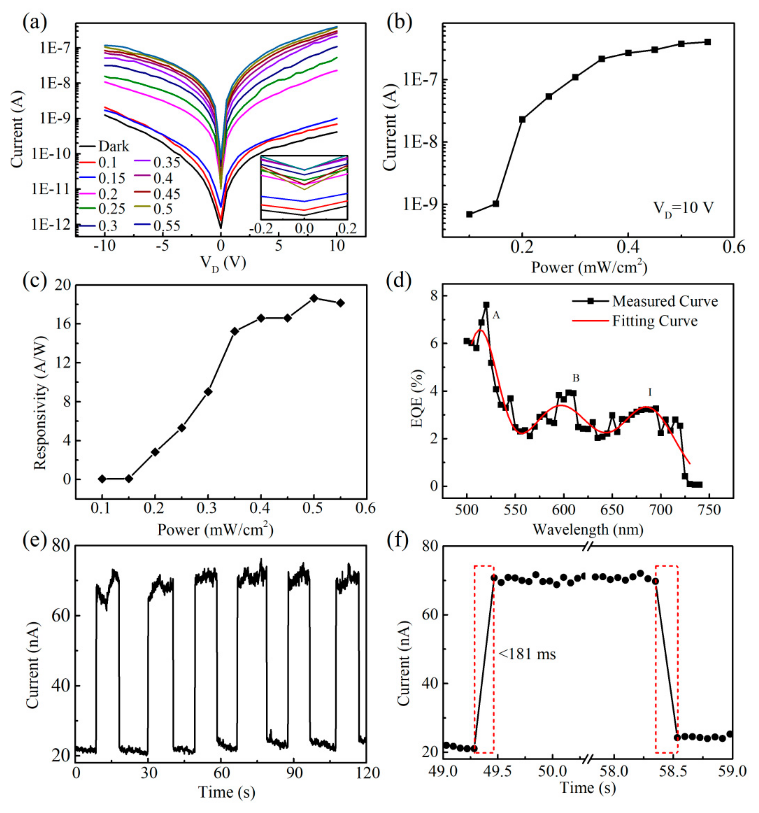
Opto-Electronic Properties of Photodetector

The linear scale of the I-V characteristics of the bilayer photodetectors was measured in the dark and under light with an intensity of 0.14 mW/cm2 and a laser excitation wavelength of 450 nm (Figure 5a). The channel width of the device was 50 μm, and the length was 200 μm. The IV curves showed a linear and symmetrical feature when no gate voltage was applied (VG = 0 V), which confirmed that the as-fabricated device had ohmic contacts between the blend film and the Cr–Au electrodes. Figure 5b shows that the photocurrent increased quickly, with the gate voltage (VG) sweeping from −30 V to 20 V. The responsivity (R) and detectivity (D*) of the aforementioned photodetectors under illumination were calculated according to
R = I l i g h t I d a r k P A ,
D * = R 2 e I d a r k A 1 / 2 ,
where Ilight is the photocurrent, Idark is the dark current, P is the light power density, A is the effective area of the photodetector, and e is the electronic charge. Figure 5c plots responsivity and detectivity, which increased with applied negative VG. On the one hand, these indices rose as the applied voltage increased, and they grew linearly when the voltage was lower than −10 V, which suggests that not only was the photocurrent far larger than the dark current (Figure 5c), but also that a quite low power (voltage) input was required to amplify the photocurrent to the highest order of magnitude. With a −30 V bias voltage, the photocurrent (Ilight) and dark current (Idark) were 2.16 × 10⁻⁸ A and 7.56 × 10⁻⁹ A, respectively. Therefore, the as-fabricated 2D WS2/Poly-TPD/PCBM/Au photodetector achieved an R of 1.01 A/W and a high D* of 1.4 × 10¹¹ Jones at the 450-nm laser excitation (VG = −30 V). The external quantum efficiency (EQE) was obtained by
E Q E = R h c e λ
where h c / λ is the photon energy. The EQE (Figure 5d) exhibited the same gate voltage dependence trend as R, reaching about 3% at VG = −30 V. As can be seen in Table 1, the obtained values in this work were comparable to those obtained in other work. Compared to WS2 devices without organic materials [60,61], our device exhibited better performance, which indicated that the organic materials could improve the 2D material photodetector performance.
Figure 6a shows the photocurrent versus applied VD sweeping from −10 V to 10 V. In addition, 10 different illumination intensities were applied to the WS2/organic device with varied laser intensities ranging from 0.1 mW/cm2 to 0.55 mW/cm2. These IV plots showed a linear increase of the photocurrent with the applied voltage. In Figure 6b, the dependence of the photocurrent (ID,light) (in Figure 6a) on the laser intensity (mW/cm2) was plotted on a log scale (VD = 10 V). The ID,light increased gradually with power intensity when the power was 0.4 mW/cm2 and then showed a saturating tendency with higher power intensity. As shown in Figure 6c, the responsivity R increased nearly linearly to 17 A/W with incident laser power when the power intensity reached 0.4 mW/cm2, and then it was gradually saturated with further increased power intensity (VD = 10 V).
The broad-spectrum response of the as-prepared bilayer photodetector was investigated with an incident laser with a wavelength varying from 500 nm to 750 nm (Figure 6d). Herein, the EQE was calculated from the IV curves (VD = 10 V and VG = 0 V), and the incident light was a 100-ps pulse laser with a 4-MHz frequency. The peaks in Figure 6d corresponded well to the A exciton (λ = 626 nm), B exciton (λ = 527 nm), and indirect band gap (I) absorption, as shown in Figure 2c, indicating that the effective absorption in the WS2 thin films actively contributed to the photocurrent generation [24,51,52]. As shown in Figure 1d, the LUMO at −4.2 eV of PCBM and the HOMO at −5.2 eV of Poly-TPD were well aligned with the conduction and valence levels of WS2 to dissociate the excitons typically generated inside the WS2 films, with an exciton binding energy of 0.3 eV to 0.7 eV [15,16]. The reliable and rapid response speed of the bilayer photodetector was examined with pulsed laser illumination, as shown in Figure 6e,f. The PD promptly responded to 450 nm of light at the millisecond level (<181 ms), giving rise to a sharply enhanced and decayed photocurrent upon multiple switching cycles.
The 2D WS2/Poly-TPD/PCBM bilayer photodetectors with few layers of WS2 could detect different photon wavelengths and a wide range of incident intensities, making it a strong candidate for constructing novel optoelectronic devices. We attribute the excellent photoresponse to the appropriate band gap, the high quality of the CVD-grown single/multilayer WS2, and the energy-favorable heterojunction. The as-prepared WS2 had excellent photon absorption throughout a wide range of 500 nm to 750 nm, allowing enough exciton (or electron-hole pair) generation. As shown in Figure 1d, 2D WS2 (conductive band edge at ca. −3.84 eV and valence band edge at ca. −5.82 eV for the monolayer) was a perfect match with the Poly-TPD/PCBM mixture (LUMO at −4.1 eV of PCBM to accept electrons and HOMO at −5.2 eV of Poly-TPD to accept holes). The energy offset of the WS2 and organic blend film (the offset between WS2 and Poly-TPD was 0.62 eV and between WS2 and PCBM was 0.26 eV) was sufficiently high enough to dissociate excitons generated from monolayer WS2, since the typical exciton binding energy was around 0.71 ± 0.01 eV [15]. Therefore, Poly-TPD was favorable for hole transport and PCBM for electron transport to their respective electrodes. Notably, Poly-TPD and PCBM were intermixed throughout the entire organic blend film, and it is highly possible that portions of the electron and hole carriers recombined first before arriving at their electrodes, resulting in a relatively low EQE when the VG = 0 V (Figure 5d). Therefore, the built-in electric field needed to be applied through the gate voltage, and more photogenerated electrons and holes could quickly drift away to their electrodes. As shown in Figure 5d, with the increase in the gate voltage applied, the current increased exponentially, which is typical diode behavior. As a result, the EQE could be modulated to 3% at VG = −30 V.
Herein, the limited trap state in the CVD-grown WS2 layer also greatly reduced the exciton quenching, and photoconductivity might have dominated the fast response time, which was consistent with the nearly linear dependence of the photocurrent on incident laser power intensity (Figure 6b). However, photocurrents higher than 0.1 uA were gradually saturated with further increased laser power intensity, indicating that the charge collection efficiency caused a limiting factor due to relatively low carrier mobility in organic blend films. Correspondingly, chances for electron and hole-free carriers under higher irradiation excitations to recombine increased before collection by their respective Au electrodes. Notably, this saturated photocurrent behavior was quite different from pure 2D WS2-sandwiched PDs, which typically have nonlinear dependence on the incident laser power intensity P0.5 [65]. As a result, the responsivity of the as-prepared bilayer 2D-WS2/organic photodetector had a saturated trend quite similar with the radiant power intensity, reaching a maximum of 17 A/W. The wide visible spectrum response (Figure 6d) clearly showed that single/multilayers of WS2 laminated with organic blend films is a promising device architecture for high-performance optoelectronic applications. Optimization of the organic blend layer conductivity will further improve this unique 2D/organic bilayer photodetector performance.

4. Conclusions

In summary, we prepared an inorganic/organic heterojunction photodetector through highly oriented 2D WS2 film and Poly-TPD/PCBM blend organic films. The results revealed that the photodetector had high responsivity and detectivity at room temperature, exhibiting a high detectivity of 1.1 × 10¹¹ Jones at zero-gate voltage and a responsivity of 17 A/W. The spin-coated organic films effectively smoothed out the WS2 films, forming an energy barrier to significantly suppress the dark current. The on/off ratio of these bilayer PDs was as high as 100, and a rise time of less than 181 ms was obtained, indicating fast electron/hole dissociation at the interface of the 2D WS2 and Poly-TPD/PCBM (1:1) organic layers. We attribute the excellent photoresponse to the appropriate band gap, the high quality of the CVD-grown single/multilayer WS2, and the energy-favorable heterojunction for efficient exciton separation. Further improvement on carrier mobility in organic layers will enhance the charge collection efficiency. Our work offers a solution-coating process combined with a CVD technique that can create high-crystalline 2D films for high-performance photodetectors over regular silicon substrates. The inorganic 2D/organic heterostructures formed will create a new and fruitful paradigm in optoelectronics.

Author Contributions

F.H., J.Z.L., Z.H.X., S.C.Z., S.W.Z., and G.D.W. conceived the idea, designed the experiments and wrote the manuscript; F.H., J.Z.L., Y.L., R.P.L., S.C.Z. and G.D.W. performed the major experiments; J.Z.L., G.D.W., Y.L., Y.F.L., S.X.Z., P.B.N., W.T.S., W.D.L., S.C.Z., G.D.W., H.C.K. and F.Y.K. each contributed to the data analysis and interpretation; All authors contributed to discussions and revision of the manuscript.

Funding

The Natural Science Foundation of Zhejiang Province, China Projects (LY16E020008); the Natural National Science Foundation of China (NSFC) (61106100); we thank the Shenzhen Municipal Development and Reform Commission and the New Energy Technology Engineering Laboratory (Grant Number: SDRC [2016]172).

Conflicts of Interest

The authors declare no conflicts of interest.

References

  1. Zhao, S.; Surwade, S.P.; Li, Z.; Liu, H. Photochemical oxidation of CVD-grown single layer graphene. Nanotechnology 2012, 23, 355703. [Google Scholar] [CrossRef] [PubMed]
  2. Zhao, S.; Zhou, F.; Li, Z.; Liu, H. Effect of precursor purity and flow rate on the CVD growth of hexagonal boron nitride. J. Alloy. Compd. 2016, 688, 1006–1012. [Google Scholar] [CrossRef]
  3. Lv, R.; Robinson, J.A.; Schaak, R.E.; Sun, D.; Sun, Y.; Mallouk, T.E.; Terrones, M. Correction to transition metal dichalcogenides and beyond: Synthesis, properties, and applications of single- and few-layer nanosheets. Acc. Chem. Res. 2015, 48, 56–64. [Google Scholar] [CrossRef] [PubMed]
  4. Xie, Z.; Wang, D.; Fan, T.; Xing, C.; Li, Z.; Tao, W.; Liu, L.; Bao, S.; Fan, D.; Zhang, H. Black phosphorus analogue tin sulfide nanosheets: Synthesis and application as near-infrared photothermal agents and drug delivery platforms for cancer therapy. J. Mater. Chem. B 2018, 6, 4747–4755. [Google Scholar] [CrossRef]
  5. Fan, T.; Zhou, Y.; Qiu, M.; Zhang, H. Black phosphorus: A novel nanoplatform with potential in the field of bio-photonic nanomedicine. J. Innov. Opt. Heal. Sci. 2018, 11, 1830003. [Google Scholar] [CrossRef] [Green Version]
  6. Guo, Z.; Chen, S.; Wang, Z.; Yang, Z.; Liu, F.; Xu, Y.; Wang, J.; Yi, Y.; Zhang, H.; Liao, L.; et al. Metal-Ion-Modified Black Phosphorus with Enhanced Stability and Transistor Performance. Adv. Mater. 2017, 29, 1703811. [Google Scholar] [CrossRef]
  7. Xing, C.; Huang, W.; Xie, Z.; Zhao, J.; Ma, D.; Fan, T.; Liang, W.; Ge, Y.; Dong, B.; Li, J.; et al. Ultrasmall Bismuth Quantum Dots: Facile Liquid-Phase Exfoliation, Characterization, and Application in High-Performance UV-Vis Photodetector. ACS Photonics 2018, 5, 621–629. [Google Scholar] [CrossRef]
  8. Fan, T.; Xie, Z.; Huang, W.; Li, Z.; Zhang, H. Two-dimensional non-layered selenium nanoflakes: Facile fabrications and applications for self-powered photo-detector. Nanotechnology 2019, 30, 114002. [Google Scholar] [CrossRef]
  9. Luo, M.; Fan, T.; Zhou, Y.; Zhang, H.; Mei, L. 2D Black Phosphorus-Based Biomedical Applications. Adv. Funct. Mater. 2019, 29, 1808306. [Google Scholar] [CrossRef]
  10. Wang, H.-D.; Sang, D.K.; Guo, Z.-N.; Cao, R.; Zhao, J.-L.; Shah, M.N.U.; Fan, T.-J.; Fan, D.-Y.; Zhang, H. Black phosphorus-based field effect transistor devices for Ag ions detection. Chin. Phys. B 2018, 27, 087308. [Google Scholar] [CrossRef]
  11. Huang, W.; Xie, Z.; Fan, T.; Li, J.; Wang, Y.; Wu, L.; Ma, D.; Li, Z.; Ge, Y.; Huang, Z.N.; et al. Black-phosphorus-analogue tin monosulfide: An emerging optoelectronic two-dimensional material for high-performance photodetection with improved stability under ambient/harsh conditions. J. Mater. Chem. C 2018, 6, 9582–9593. [Google Scholar] [CrossRef]
  12. Cao, R.; Wang, H.D.; Guo, Z.N.; Sang, D.K.; Zhang, L.Y.; Xiao, Q.L.; Zhang, Y.P.; Fan, D.Y.; Li, J.Q.; Zhang, H. Black Phosphorous Photodetectors: Black Phosphorous/Indium Selenide Photoconductive Detector for Visible and Near Infrared Light with High Sensitivity. Adv. Opt. Mater. 2019, 7, 1970047. [Google Scholar] [CrossRef]
  13. Li, N.; Feng, L.P.; Su, J.; Zeng, W.; Liu, Z.T. Optical and electrical properties of Al:WS2 films prepared by atomic layer deposition and vulcanization. RSC Adv. 2016, 6, 64879–64884. [Google Scholar] [CrossRef]
  14. Park, J.; Kim, M.S.; Cha, E.; Kim, J.; Choi, W. Synthesis of uniform single layer WS2 for tunable photoluminescence. Sci. Rep. 2017, 7, 16121. [Google Scholar] [CrossRef] [PubMed]
  15. Zhu, B.; Chen, X.; Cui, X. Exciton Binding Energy of Monolayer WS2. Sci. Rep. 2015, 5, 9218. [Google Scholar] [CrossRef] [PubMed]
  16. Chernikov, A.; Berkelbach, T.C.; Hill, H.M.; Rigosi, A.; Li, Y.; Aslan, O.B.; Reichman, D.R.; Hybertsen, M.S.; Heinz, T.F. Exciton Binding Energy and Nonhydrogenic Rydberg Series in MonolayerWS2. Phys. Rev. Lett. 2014, 113, 076802. [Google Scholar] [CrossRef] [PubMed]
  17. Kotadiya, N.B.; Lü, H.; Mondal, A.; Ie, Y.; Andrienko, D.; Blom, P.W.M.; Wetzelaer, G.-J.A. Universal strategy for Ohmic hole injection into organic semiconductors with high ionization energies. Nat. Mater. 2018, 17, 329. [Google Scholar] [CrossRef] [PubMed]
  18. Li, D.; Lai, W.-Y.; Zhang, Y.-Z.; Huang, W. Printable Transparent Conductive Films for Flexible Electronics. Adv. Mater. 2018, 30, 1704738. [Google Scholar] [CrossRef] [PubMed]
  19. Yang, M.; Wang, J.; Zhao, Y.; He, L.; Ji, C.; Liu, X.; Zhou, H.; Wu, Z.; Wang, X.; Jiang, Y. Three-dimensional topological Insulator Bi2Te3/organic thin film heterojunction photodetector with fast and wideband response from 450 to 3500 Nanometers. ACS Nano 2019, 13, 755–763. [Google Scholar] [CrossRef] [PubMed]
  20. Zhang, H.; Song, L.; Luo, L.; Liu, L.; Wang, H. TiO2/Sb2S3/P3HT Based Inorganic-Organic Hybrid Heterojunction Solar Cells with Enhanced Photoelectric Conversion Performance. J. Electron. Mater. 2017, 46, 4670–4675. [Google Scholar] [CrossRef]
  21. Trzcinski, K.; Szkoda, M.; Siuzdak, K.; Sawczak, M.; Lisowska-Oleksiak, A. Enhanced photoelectrochemical performance of inorganic-organic hybrid consisting of BiVO4 and PEDOT:PSS. Appl. Surf. Sci. 2016, 388, 753–761. [Google Scholar] [CrossRef]
  22. Dai, X.; Shi, C.; Zhang, Y.; Wu, N. Hydrolysis preparation of the compact TiO2 layer using metastable TiCl4 isopropanol/water solution for inorganic-organic hybrid heterojunction perovskite solar cells. J. Semicond. 2015, 36, 7. [Google Scholar] [CrossRef]
  23. Lv, Y.; Huang, F.; Zhang, L.; Weng, J.; Zhao, S.; Ji, Z. Preparation and Photoluminescence of Tungsten Disulfide Monolayer. Coatings 2018, 8, 205. [Google Scholar] [CrossRef]
  24. Gutiérrez, H.R.; Perea-López, N.; Elías, A.L.; Berkdemir, A.; Wang, B.; Lv, R.; López-Urías, F.; Crespi, V.H.; Terrones, H.; Terrones, M. Extraordinary Room-Temperature Photoluminescence in Triangular WS2 Monolayers. Nano Lett. 2013, 13, 3447–3454. [Google Scholar] [CrossRef] [PubMed]
  25. Liu, P.; Luo, T.; Xing, J.; Xu, H.; Hao, H.; Liu, H.; Dong, J. Large-Area WS2 Film with Big Single Domains Grown by Chemical Vapor Deposition. Nanoscale Res. Lett. 2017, 12, 558. [Google Scholar] [CrossRef] [PubMed]
  26. Peimyoo, N.; Shang, J.; Cong, C.; Shen, X.; Wu, X.; Yeow, E.K.L.; Yu, T. Nonblinking, Intense Two-Dimensional Light Emitter: Monolayer WS2 Triangles. ACS Nano 2013, 7, 10985–10994. [Google Scholar] [CrossRef]
  27. Lan, F.; Yang, R.; Xu, Y.; Qian, S.; Zhang, S.; Cheng, H.; Zhang, Y. Synthesis of Large-Scale Single-Crystalline Monolayer WS2 Using a Semi-Sealed Method. Nanomaterials 2018, 8, 100. [Google Scholar] [CrossRef] [PubMed]
  28. Chan, K.H.; Ng, S.M.; Wong, H.F.; Leung, C.W.; Mak, C.L. Rectify effect of Pedot:PSS/WS2 heterostructure. Phys. Status Solidi A 2019, 216, 1800829. [Google Scholar] [CrossRef]
  29. Yan, J.; Hao, Y.; Cui, Y.; Zhang, J.; Zou, Y.; Zhang, W.; Yu, G.; Zheng, J.; Xu, W.; Zhu, D. Ambipolar charge transport in an organic/inorganic van der Waals p-n heterojunction. J. Mater. Chem. C 2018, 6, 12976–12980. [Google Scholar] [CrossRef]
  30. Shen, Y.; Yu, D.; Wang, X.; Huo, C.; Wu, Y.; Zhu, Z.; Zeng, H. Two-dimensional CsPbBr3/PCBM heterojunctions for sensitive, fast and flexible photodetectors boosted by charge transfer. Nanotechnology 2018, 29, 085201. [Google Scholar] [CrossRef]
  31. Homan, S.B.; Sangwan, V.K.; Balla, I.; Bergeron, H.; Weiss, E.A.; Hersam, M.C. Ultrafast Exciton Dissociation and Long-Lived Charge Separation in a Photovoltaic Pentacene MoS2 van der Waals Heterojunction. Nano Lett. 2017, 17, 164–169. [Google Scholar] [CrossRef] [PubMed]
  32. Yao, D.; Zhang, C.; Zhang, S.; Yang, D.A.; Eric, W.; Yu, X.; Wilson Gregory, J.; Wang, H. 2D-3D mixed organic-inorganic perovskite layers for solar cells with enhanced efficiency and stability induced by n-Propylammonium iodide additives. ACS Appl. Mater. Interfaces 2019, 11, 29753–29764. [Google Scholar] [CrossRef] [PubMed]
  33. Li, Y.; Shu, J.; Huang, Q.; Chiranjeevulu, K.; Kumar, P.N.; Wang, G.E.; Deng, W.H.; Tang, D.; Xu, G. 2D metal chalcogenides with surfaces fully covered with an organic “promoter” for high-performance biomimetic catalysis. Chem. Commun. 2019, 55, 10444–10447. [Google Scholar] [CrossRef]
  34. Ba, Q.; Jana, A.; Wang, L.; Kim, K.S. Dual emission of water-stable 2D organic-inorganic halide perovskites with Mn(II) dopant. Adv. Funct. Mater. 2019, 8, 1904768. [Google Scholar] [CrossRef]
  35. Chiang, C.-H.; Wu, C.-G. Bulk heterojunction perovskite-PCBM solar cells with high fill factor. Nat. Photonics 2016, 10, 196–200. [Google Scholar] [CrossRef]
  36. Wang, X.; Wang, J.Y.; Zhao, H.M.; Jin, H.; Yu, J.S. Detectivity enhancement of double-layer organic photodetectors consisting of solution-processed interconnecting layers. Mater. Lett. 2019, 243, 81–83. [Google Scholar] [CrossRef]
  37. Blankenburg, L.; Sensfuss, S.; Schache HMarten, J.; Milker, R.; Schrodner, M. TPD wide-bandgap polymers for solar cell application and their sensitization with small molecule dyes. Synth. Met. 2015, 199, 93–104. [Google Scholar] [CrossRef]
  38. Yang, X.; Divayana, Y.; Zhao, D.; Leck, K.S.; Lu, F.; Tan, S.T.; Abiyasa, A.P.; Zhao, Y.; Demir, H.V.; Sun, X.W. A bright cadmium-free, hybrid organic/quantum dot white light-emitting diode. Appl. Phys. Lett. 2012, 101, 233110. [Google Scholar] [CrossRef]
  39. Kang, J.; Tongay, S.; Zhou, J.; Li, J.B.; Wu, J.Q. Band offsets and heterostructures of two-dimensional semiconductors. Appl. Phys. Lett. 2013, 102, 012111. [Google Scholar] [CrossRef]
  40. Muhlbacher, D.; Scharber, M.; Morana, M.; Zhu, Z.G.; Waller, D.; Gaudiana, R.; Brabec, C. High photovoltaic performance of a low-bandgap polymer. Adv. Mater. 2006, 18, 2884–2889. [Google Scholar] [CrossRef]
  41. Raja, A.; Selig, M.; Berghauser, G.; Yu, J.; Hill, H.M.; Rigosi, A.F.; Brus, L.E.; Knorr, A.; Heinz, T.F.; Malic, E.; et al. Enhancement of exciton-phonon scattering from monolayer to bilayer WS2. Nano Lett. 2018, 18, 6135–6143. [Google Scholar] [CrossRef] [PubMed]
  42. Du, L.; Jia, Z.; Zhang, Q.; Zhang, A.; Zhang, T.; He, R.; Yang, R.; Shi, D.; Yao, Y.; Xiang, J.; et al. Electronic structure-dependent magneto-optical Raman effect in atomically thin WS2. 2D Mater. 2018, 5, 035028. [Google Scholar] [CrossRef]
  43. Zhu, D.; Zhu, Q.; Gu, C.; Ouyang, D.; Qiu, M.; Bao, X.; Yang, R. Alkoxyl Side Chain Substituted Thieno[3,4-c]pyrrole-4,6-dione To Enhance Photovoltaic Performance with Low Steric Hindrance and High Dipole Moment. Macromolecules 2016, 49, 5788–5795. [Google Scholar] [CrossRef]
  44. Ji, Z.; Mao, Q.; Ke, W. Effects of oxygen partial pressure on resistive switching characteristics of ZnO thin films by DC reactive magnetron sputtering. Materials 2010, 150, 1919–1922. [Google Scholar] [CrossRef]
  45. Jin, S.Z.; Zhao, S.C.; Weng, J.X.; Lv, Y.F. Mn-promoted growth and photoluminescence of molybdenum disulphide monolayer. Coatings 2017, 7, 78. [Google Scholar] [CrossRef]
  46. Li, J.; Su, W.; Chen, F.; Fu, L.; Ding, S.; Song, K.; Huang, X.; Zhang, L. Atypical Defect-Mediated Photoluminescence and Resonance Raman Spectroscopy of Monolayer WS2. J. Phys. Chem. C 2019, 123, 3900–3907. [Google Scholar] [CrossRef]
  47. Xu, Z.; Lv, Y.; Huang, F.; Zhao, C.; Zhao, S.; Wei, G. ZnO-Controlled Growth of Monolayer WS2 through Chemical Vapor Deposition. Materials 2019, 12, 1883. [Google Scholar] [CrossRef]
  48. Pawbake, A.S.; Waykar, R.G.; Late, D.J.; Jadkar, S.R. Highly transparent wafer-scale synthesis of crystalline WS2 nanoparticle thin film for photodetector and humidity-sensing applications. ACS Appl. Mater. Interfaces 2016, 8, 3359–3365. [Google Scholar] [CrossRef]
  49. Ji, Z.; Zhao, S.; Wang, C.; Liu, K. ZnO nanoparticle films prepared by oxidation of metallic zinc in H2O2 solution and subsequent process. Mater. Sci. Eng. B 2005, 117, 63–66. [Google Scholar] [CrossRef]
  50. Dong, W.; Shi, J.L.; Wang, T.S.; Yin, Y.X.; Wang, C.R.; Guo, Y.G. 3D zinc@carbon fiber composite framework anode for aqueous Zn-MnO2 batteries. RSC Adv. 2018, 8, 19157–19163. [Google Scholar] [CrossRef]
  51. Ballif, C.; Regula, M.; Schmid, P.E.; Remskar, M.; Sanjines, R.; Levy, F. Preparation and characterization of highly oriented, photoconducting WS2 thin films. Appl. Phys. A 1996, 62, 543–546. [Google Scholar] [CrossRef]
  52. Sasaki, S.; Kobayashi, Y.; Liu, Z.; Suenaga, K.; Maniwa, Y.; Miyauchi, Y.; Miyata, Y. Growth and optical properties of Nb-doped WS2 monolayers. Appl. Phys. Express 2016, 9, 071201. [Google Scholar] [CrossRef]
  53. Ramasubramaniam, A. Large excitonic effects in monolayers of molybdenum and tungsten dichalcogenides. Phys. Rev. B 2012, 86, 115409. [Google Scholar] [CrossRef]
  54. Zhao, W.J.; Ghorannevis, Z.; Chu, L.Q.; Toh, M.L.; Kloc, C.; Tan, P.H.; Eda, G. Evolution of electronic structure in atomically thin sheets of WS2 and WSe2. ACS Nano. 2013, 7, 791–797. [Google Scholar] [CrossRef] [PubMed]
  55. Peimyoo, N.; Yang, W.H.; Shang, J.Z.; Shen, X.N.; Wang, Y.L.; Yu, T. Chemically driven tunable light emission of charged and neutral excitons in mono layer WS2. ACS Nano 2014, 8, 11320–11329. [Google Scholar] [CrossRef] [PubMed]
  56. Berkdemir, A.; Gutiérrez, H.R.; Botello-Méndez, A.R.; Perea-López, N.; Elías, A.L.; Chia, C.-I.; Wang, B.; Crespi, V.H.; López-Urías, F.; Charlier, J.-C.; et al. Identification of individual and few layers of WS2 using Raman Spectroscopy. Sci. Rep. 2013, 3, 1755. [Google Scholar] [CrossRef]
  57. Zhao, W.; Ghorannevis, Z.; Amara, K.K.; Pang, J.R.; Toh, M.; Zhang, X.; Kloc, C.; Tan, P.H.; Eda, G. Lattice dynamics in mono- and few-layer sheets of WS2 and WSe2. Nanoscale 2013, 5, 9677. [Google Scholar] [CrossRef]
  58. Yun, S.J.; Chae, S.H.; Kim, H.; Park, J.C.; Park, J.-H.; Han, G.H.; Lee, J.S.; Kim, S.M.; Oh, H.M.; Seok, J.; et al. Synthesis of Centimeter-Scale Monolayer Tungsten Disulfide Film on Gold Foils. ACS Nano 2015, 9, 5510–5519. [Google Scholar] [CrossRef]
  59. Li, Y.; Li, X.; Yu, T.; Yang, G.; Chen, H.; Zhang, C.; Feng, Q.; Ma, J.; Liu, W.; Xu, H.; et al. Accurate identification of layer number for few-layer WS2 and WSe2 via spectroscopic study. Nanotechnology 2018, 29, 124001. [Google Scholar] [CrossRef]
  60. Esfandiari, M.; Mohajerzadeh, S.; Mohajerzadeh, S. Formation of large area WS2 nanosheets using an oxygen-plasma assisted exfoliation suitable for optical devices. Nanotechnology 2019, 30, 425204. [Google Scholar] [CrossRef]
  61. Yao, J.; Shao, J.; Zheng, Z.; Yang, G. Stable, high-responsive and broadband photodetection based on large-area multilayer WS2 films grown by pulsed-laser deposition. Nanoscale 2015, 7, 14974–14981. [Google Scholar] [CrossRef] [PubMed]
  62. Lai, J.; Liu, X.; Ma, J.; Wang, Q.; Zhang, K.; Ren, X.; Liu, Y.; Gu, Q.; Zhuo, X.; Lu, W.; et al. Anisotropic Broadband Photoresponse of Layered Type-II Weyl Semimetal MoTe2. Adv. Mater. 2018, 30, 1707152. [Google Scholar] [CrossRef] [PubMed]
  63. Yang, Y.; Liu, S.-C.; Yang, W.; Li, Z.; Wang, Y.; Wang, X.; Zhang, S.; Zhang, Y.; Long, M.; Zhang, G.; et al. Air-Stable In-Plane Anisotropic GeSe2 for Highly Polarization-Sensitive Photodetection in Short Wave Region. J. Am. Chem. Soc. 2018, 140, 4150–4156. [Google Scholar] [CrossRef] [PubMed]
  64. Li, L.; Wang, W.; Gong, P.; Zhu, X.; Deng, B.; Shi, X.; Gao, G.; Li, H.; Zhai, T. 2D GeP: An Unexploited Low-Symmetry Semiconductor with Strong In-Plane Anisotropy. Adv. Mater. 2018, 30, e1706771. [Google Scholar] [CrossRef] [PubMed]
  65. Perea-López, N.; Elías, A.L.; Berkdemir, A.; Castro-Beltran, A.; Gutiérrez, H.R.; Feng, S.M.; Lv, R.T.; Hayashi, T.; López-Urías, F.; Ghosh, S.; et al. Photosensor device based on few-layered WS2 films. Adv. Funct. Mater. 2013, 23, 5511–5517. [Google Scholar] [CrossRef]
Figure 1. Illustration (color online) of the fabrication procedure of the photodetector based on the organic semiconductor/inorganic tungsten disulfide (WS2) heterojunction. (a) The silicon substrate with ZnO and SiO2 film (ZnO/SiO2/Si). (b) Two-dimensional (2D) WS2 growth on the surface of SiO2/Si through a chemical vapor deposition (CVD) method. During the growth of the WS2, ZnO was removed from the SiO2/Si. (c) (Poly-(N,N′-bis-4-butylphenyl-N,N′-bisphenyl) benzidine and Phenyl-C61-butyric acid methyl ester (Poly-TPD/PCBM) (1:1) organic film preparation by spin-coating on the surface of the 2D WS2. (d) Metal electrode evaporation on the surface of the Poly-TPD/PCBM film.
Nanomaterials 09 01312 g001
Figure 2. (a) The X-ray diffraction (XRD) spectra of the ZnO/SiO2/Si substrate (black line) and WS2 film (red line). (b) X-ray photoelectron spectroscopy (XPS) spectrum of the WS2 film. UV-Vis absorption spectrum of the (c) WS2 film and (d) Poly-TPD/PCBM (1:1).
Nanomaterials 09 01312 g002
Figure 3. (a,b) Typical field emission scanning electron microscopy (FESEM) images of the WS2 film. Images (a,b) were taken at different locations. (c) Atomic force microscope (AFM) image of 1:1 Poly-TPD and PCBM mixture.
Nanomaterials 09 01312 g003
Figure 4. The Raman (a) and photoluminescence (PL) spectra (b) of the WS2 monolayer (red line) and multilayers (blue line). Inset in (a) is a detailed illustration of the B2g1 and A1g modes. The insert in (b) is an SEM image, and the scale bar represents 5 μm. (c) Photoluminescence (PL) and (d) optical microscopy images of WS2 mono-/multimixed layers taken at the same location.
Nanomaterials 09 01312 g004
Figure 5. Performance of the WS2/Poly-TPD/PCBM-based photodetector. (a) Source-drain current (ID) versus drain voltage (VD). (b) ID versus gate voltage (VG) curves of the photodetector in dark (black line) and under laser (red line). (c,d) Responsivity and detectivity curves and the external quantum efficiency (EQE) of the device as a function of VG ranging from −30 V to 20 V. Measurements were performed at room temperature with a laser at 450 nm. The light intensity was 0.14 mW/cm2. The VG was 0 V in (a), and the VD was 15 V in (b–d).
Nanomaterials 09 01312 g005
Figure 6. (a) The photocurrent versus applied VD sweeping from −10 V to 10 V (VG = 0 V) at different light intensities. The inset shows the detailed IV characteristics in the 0 V region. (b) The dependence of the photocurrent (ID,light) (in (a)) on the laser intensity (mW/cm2) (VG = 0 V, VD = 10 V). (c) Power intensity dependence of the responsivity (VG = 0 V, VD = 10 V). (d) Spectral dependence of the EQE using a 100-ps pulse laser (VG = 0 V, VD = 10 V). (e) Photoresponse in the dark and under 450-nm laser irradiation with a light intensity of 0.14 mW/cm2 (VG = 0 V, VD = 10 V). (f) Rise and decay time of the photodetector (VG = 0 V, VD = 10 V).
Nanomaterials 09 01312 g006
Table 1. Photoresponse parameters of different materials and devices.
Device StructureIncident LightR (A/W)D (Jones)Response TimeRef.
2D WS2/Poly-TPD/PCBM/Au450 nm1.021.4 × 1011<181 msThis work
Monolayer WS2/Au532 nm0.596.5 × 1010280 ms[60]
Multilayer WS2/Au635 nm0.72.7 × 10104.1 s[61]
MoTe2/Au532 nm0.00041.08 × 10842.5 μs[62]
GeSe2/Au450 nm2.5 N/A0.2 s[63]
GeP/Au532 nm3.1N/A>1s[64]

