Article

Mg Doped CuCrO2 as Efficient Hole Transport Layers for Organic and Perovskite Solar Cells

1
Department of Materials Science and Engineering, The University of Texas at Dallas, Richardson, TX 75080, USA
2
Department of Mechanical Engineering and Materials Science, Duke University, Durham, NC 27708, USA
3
Department of Physics, The University of Texas at Dallas, Richardson, TX 75080, USA
4
Department of Applied Chemistry, National Chiao Tung University, 1001 University Road, Hsinchu 30010, Taiwan
*
Author to whom correspondence should be addressed.
Nanomaterials 2019, 9(9), 1311; https://doi.org/10.3390/nano9091311
Submission received: 19 July 2019 / Revised: 9 September 2019 / Accepted: 11 September 2019 / Published: 13 September 2019

Abstract

:
The electrical and optical properties of the hole transport layer (HTL) are critical for organic and halide perovskite solar cell (OSC and PSC, respectively) performance. In this work, we studied the effect of Mg doping on CuCrO2 (CCO) nanoparticles and their performance as HTLs in OSCs and PSCs. CCO and Mg doped CCO (Mg:CCO) nanoparticles were hydrothermally synthesized. The nanoparticles were characterized by various experimental techniques to study the effect of Mg doping on structural, chemical, morphological, optical, and electronic properties of CCO. We found that Mg doping increases work function and decreases particle size. We demonstrate CCO and Mg:CCO as efficient HTLs in a variety of OSCs, including the first demonstration of a non-fullerene acceptor bulk heterojunction, and CH3NH3PbI3 PSCs. A small improvement of average short-circuit current density with Mg doping was found in all systems.

1. Introduction

With continued increase in power conversion efficiency (PCE), organic and perovskite solar cells (OSCs and PSCs, respectively) are promising for low cost clean electricity generation [1,2,3]. Further enhancing the PCE of OSCs and PSCs requires not only the development of better absorber materials, but also suitable transport layer materials. In OSCs and PSCs, the absorber is sandwiched between an electron transport layer (ETL) and a hole transport layer (HTL), whose primary functions are to set up the built-in field across the absorber and selectively extract their respective carriers, while blocking the other type of carriers. In bulk heterojunction (BHJ) OSCs, the photogenerated excitons dissociate at the donor/acceptor interface to charged carriers. In PSCs, photoabsorption directly generates electrons and holes. These carriers then drift in opposite directions due to the built-in electric field, and travel through the transport layers to the electrodes [4]. Thus, both ETL and HTL play an important role in carrier extraction and device performance. For effective hole extraction from the absorber, the material used as HTL should possess good optical and electrical properties in addition to good physical and chemical stability. Extensive studies have been devoted to organic materials, such as poly(3,4-ethylenedioxythiophene) polystyrene sulfonate and 2,2′,7,7′-Tetrakis[N,N-di(4-methoxyphenyl)amino]-9,9′-spirobifluorene, as HTLs [5,6,7]. However, these materials are expensive and degrade under air exposure [8,9]. Alternatively, metal oxides are shown to be promising candidates for HTL due to their low cost and improved stability [10]. Commonly used metal oxides are MoOx and WO3 [11,12], but these n-type semiconductors do not block electrons [13,14]. Among p-type HTLs, NiOx has been shown to have promising performance [15,16]. However, it suffers from low conductivity and high visible light absorption [17,18]. Therefore, developing new inorganic p-type HTLs is crucial to achieve highly efficient and stable devices.
Delafossite (AMO2; A = Cu1+ or Ag1+ and M is a trivalent metal) compounds are p-type oxides and have drawn significant interest since Kawazoe et al. reported CuAlO2 as a transparent oxide with room temperature conductivity up to 1 S cm−1 [19]. Since then, many Cu-based delafossites have been synthesized with M = Al, Sc, Cr, Mn, Fe, Co, Ga, and Rh [20]. CuCrO2 (CCO) is particularly attractive due to its high conductivity [21]. Theoretical calculations and X-ray photoelectron spectroscopy (XPS) studies showed that Cu d states are dominant at the valence band maximum (VBM) and the intrinsic CCO conduction is through a CuI/CuII mixed valence hole mechanism [22,23]. The size of CCO nanoparticles can be very small, ~10 nm [24,25]. In solar energy harvesting, it was first used in p-type dye sensitized solar cells (DSSCs) [25]. Moreover, CCO has been shown as a promising HTL in OSCs and PSCs [24,26,27,28,29]. To further increase the hole concentration, efforts have been made to replace the trivalent Cr3+ cation with a divalent dopant such as Ni2+, Mg2+, or Zn2+ [30,31,32]. In particular, Mg has been shown to be an excellent dopant to increase CCO conductivity [22,31,33]. Theoretical calculations showed that Mg doping induces low-formation energy defects just above the VBM in CCO and introduces new Cu d states in the bandgap, thus leading to a CuI/CuII mixed valence and higher conductivity [22,33]. Compared with Be and Ca, defect states introduced by Mg are closest to the VBM, making it a more effective dopant [34]. Several experimental studies also confirm that Mg doping increases electrical conductivity [31,35,36,37]. In p-type DSSCs, Mg doped CCO (Mg:CCO) has performed superior to undoped CCO [38,39].
Based on our results of using undoped CCO as HTL in OSCs [24] and PSCs [27], we hypothesized that Mg:CCO could further improve the solar cell performance. Mg:CCO has not been applied as HTL in OSCs and, to our knowledge, there is only one report of using Mg:CCO as HTL in PSCs [40]. In this work, we examine the effect of Mg doping on CCO nanoparticles and their performance as HTLs in OSCs and PSCs. The CCO and Mg:CCO nanoparticles are synthesized by a hydrothermal method. The influence of Mg doping on structural, chemical, morphological, optical, and electronic properties of CCO films are carefully characterized by X-ray diffraction (XRD), energy-dispersive X-ray spectroscopy (EDX), transmission electron microscopy (TEM), dynamic light scattering (DLS), X-ray photoelectron spectroscopy (XPS), scanning electron microscopy (SEM), ultraviolet–visible (UV-vis) absorption spectrometry, photo-electron spectroscopy in air (PESA), and Kelvin probe (KP) techniques. Finally, spin-coated CCO and Mg:CCO nanoparticle films are used as HTLs in three different BHJ OSCs and methylammonium lead iodide (MAPbI3) PSCs. Time-resolved photoluminescence (TRPL) is applied to probe charge transfer between MAPbI3 and HTL, and XPS is used to examine elemental diffusion. This is the first work to apply Mg:CCO nanoparticle films as HTLs in OSCs and the first demonstration in a non-fullerene acceptor BHJ system.

2. Materials and Methods

The chemicals used in this study included copper(II) nitrate hemipentahydrate (Cu(NO3)2·2.5 H2O, Alfa Aesar, ACS, 98.0–102.0%, Tewksbury, MA, USA), chromium(III) nitrate nonahydrate (Cr(NO3)3·9 H2O, Alfa Aesar, 98.5%, Tewksbury, MA, USA), magnesium nitrate hydrate (Mg(NO3)2, Avocado Research Chemicals, 99.999%, London, United Kingdom), sodium hydroxide (NaOH, Sigma Aldrich, ≥97.0%, St. Louis, MO, USA), hydrochloric acid (HCl, Fisher Scientific, 37%, Houston, TX, USA), ethanol (EtOH, Fisher Chemical, anhydrous, Houston, TX, USA), 2-methoxyethanol (2-MOE, Acros Organics, 99+%, Houston, TX, USA), acetone (Fisher Chemical, certified ACS, Houston, TX, USA), 2-propanol (IPA, Fisher Chemical, certified ACS plus, Houston, TX, USA), poly(3-hexylthiophene-2,5-diyl) (P3HT, Rieke Metals, LLC, ≥96%, Lincoln, NE, USA), [6:6]-phenyl C61-butyric acid methyl ester (PC61BM, Solenne BV, >99%, Groningen, The Netherlands), [6,6]-phenyl C71-butyric acid methyl ester (PC71BM, Solenne BV, >99%, Groningen, The Netherlands), poly(5-bromo-4-(2-octyldodecyl)-selenophen2-yl)-5,6-difluorobenzothiadiazole-5,5′-bis-(trimethylstannyl)-2,2′-bithiophene (PFBT2Se2Th), poly[4,8-bis(5-(2-ethylhexyl)thiophen-2-yl)benzo[1,2-b;4,5-b’]dithiophene-2,6-diyl-alt-(4-(2-ethylhexyl)-3-fluorothieno[3,4-b]thiophene-)-2-carboxylate-2-6-diyl)] (PTB7-Th, Luminescence Technology Corp., New Taipei City, Taiwan), 3,9-bis(2-methylene-(3-(1,1-dicyanomethylene)-indanone))-5,5,11,11-tetrakis(4-hexylphenyl)-dithieno[2,3-d:2′,3′-d’]-s-indaceno[1,2-b:5,6-b’]dithiophene (ITIC, 1-Material Inc., Dorval, QC, Canada), chlorobenzene (CB, Sigma-Aldrich, anhydrous, 99.8%, St. Louis, MO, USA), 1,4-dichlorobenzene (DCB, Sigma Aldrich, anhydrous, 99%, St. Louis, MO, USA), diphenyl ether (DPE, Acros Organics, 99%, Houston, TX, USA), chloroform (CF, Sigma-Aldrich, ACS reagent, ≥99.8%, St. Louis, MO, USA), lead(II) iodide (TCI, 99.99%, Portland, OR, USA), methylammonium iodide (Dyesol, Queanbeyan, NSW, Australia), potassium iodide (Alfa Aesar, 99.998%, Tewksbury, MA, USA), dimethylformamide and dimethyl sulfoxide (DMF and DMSO, Sigma Aldrich, anhydrous grade, St. Louis, MO, USA), C60 (Luminescence Technology Corp., >99.5%, New Taipei City, Taiwan), and bathocuproine (BCP) (Sigma Aldrich, sublimed grade, 99.99%, St. Louis, MO, USA). All chemicals were used without further purification. PFBT2Se2Th was prepared according to previous publication, via copolymerization of 4,7-Bis(5-bromo-4-(2-octyldodecyl)selenophen-2-yl)-5,6-difluorobenzothiadiazole (FBT2Se) and 5,5′-bis(trimethylstannyl)-2,2′-bithiophene (2Th) [41].

2.1. CuCrO2 (CCO) and Mg:CCO Preparation

2.1.1. Nanoparticle Synthesis

Mg:CCO nanoparticles with 0 at%, 5 at%, and 10 at% Mg doping levels were synthesized by a hydrothermal method as reported in previous literature [39]. First, 7.5 mmol Cu(NO3)2·2.5H2O and stoichiometric amounts of Cr(NO3)3·9H2O and Mg(NO3)2 were dissolved in 35 mL deionized (DI) water and stirred for 15 min at room temperature. Next, 2.5 g NaOH was added into the mixture and stirred for another 15 min at room temperature. The precursor solution was transferred into a 50 mL autoclave reactor (Col-Int Tech., Irmo, SC, USA), filled to 70% of its total volume. The hydrothermal reaction was carried out at 240 °C for CCO and 230 °C for Mg:CCO for 60 hours. Finally, the precipitate was washed using 2 M HCl and EtOH in sequence several times until the supernatant was colorless. After centrifuging, the mud was dried in a desiccator at room temperature overnight to obtain CCO or Mg:CCO powders.

2.1.2. Suspension Preparation

CCO and Mg:CCO nanoparticles were dispersed into 2-MOE to make 2 mg mL−1 suspensions for materials characterization and fabrication of P3HT:PC61BM OSCs, PFBT2Se2Th:PC71BM OSCs, PTB7-Th:ITIC OSCs, and MAPbI3 PSCs. Just prior to film preparation, the suspensions were placed into a bath sonicator (Branson 3510, Plano, TX, USA) for 90 min, then filtered through a 1 μm PTFE filter (Thermos scientific, Titan3, Houston, TX, USA), re-sonicated for 90 min, and again filtered through a 0.45 μm PTFE filter (Biomed Scientific, Seattle, WA, USA).

2.1.3. Film Preparation

2 mg mL−1 CCO and Mg:CCO suspensions were drop cast on gold-coated silicon substrates for EDX (Zeiss Supra 40) and XPS and on Cu grids (Ted Pella, Inc., Redding, CA, USA) for TEM imaging. CCO and Mg:CCO suspensions were spin coated multiple times on glass substrates for UV-vis (Ocean Optics USB 4000, Largo, FL, USA), spectroscopic ellipsometry (J. A. Woollam M-2000DI, Lincoln, NE, USA), and PESA (RKI Instruments Model AC-2, Union City, CA, USA), and on ITO substrates for SEM (Zeiss Supra 40, Lewisville, TX, USA) and KP (KP Technology SKP 5050, Caithness, Scotland) measurements and solar cells. After spin coating, the CCO and Mg:CCO films were annealed on a hot plate (120–175 °C) for 5 min in air to evaporate the solvent.

2.2. Materials Characterizaton

The crystalline phases of the nanoparticles were characterized by XRD using a Rigaku Ultima III diffractometer (The Woodlands, TX, USA) with Cu Kα (λ = 1.5418 Å) radiation. Powder diffraction files (PDFs) were used to identify characteristic peaks in the XRD patterns. Polytype compositions, crystal size and lattice parameters of XRD patterns were performed using Profex (an open source XRD and Rietveld refinement software, Solothurn, Switzerland) and structure files for phase identification were downloaded from the Crystallography Open Database (COD). The film morphologies were examined using SEM. The experimental Mg doping concentration was quantified using EDX. Nanoparticle size was measured from TEM images from the Delong LVEM5 Benchtop Electron Microscope (Delong TEM, Montreal, QC, Canada) equipped with the Q-Capture Pro 7 software. Hydrodynamic sizes were measured by DLS using a Malvern Zetasizer Nano ZS instrument (Malvern, United Kingdom). The lattice fringe distances were determined from high resolution TEM (HR TEM) images of nanoparticles obtained using a JEOL JEM2100 TEM (Peabody, MA, USA). The elemental compositions and chemical states of the films were analyzed by XPS, using a PHI 5000 Versa Probe II equipped with an Al Kα source and a hemispherical analyzer. XPS data were taken at a 45° takeoff angle with a pass energy of 23.5 eV. Optical transmission of the films was characterized by UV-vis over the wavelength range from 178 to 890 nm. The band gap energy was determined from Tauc plots of the UV-vis absorbance data. Film thickness was obtained by ellipsometry at 55°, 65°, and 75° incident angles over the wavelength range from 280 to 1690 nm. Ionization energy was measured from 4.7 to 5.8 eV with a 0.05 eV energy step using PESA with deuterium lamp intensity at 100 nW. The work function was measured using a KP apparatus (SKP5050, KP Technology) referenced to Au at 5.15 eV.

2.3. Solar Cell Fabrication and Testing

2.3.1. P3HT:PC61BM OSCs

P3HT:PC61BM devices were fabricated on patterned ITO substrates (Xinyan Technology Ltd., Kwun Tong, Hong Kong, 15 Ω sq−1). The substrates were rinsed using soapy water, acetone, and IPA, followed by UV-ozone treatment for 20 min. 2 mg mL−1 CCO and Mg:CCO suspensions were spin coated at 2000 rpm for 30 s on top of the ITO substrates. The thickness of CCO and Mg:CCO nanoparticle films are ~18 nm; see Section 3.2 for details. 23 mg mL−1 P3HT and 23 mg mL−1 PC61BM were dissolved in CB and stirred at 50 °C overnight. The P3HT:PC61BM active layer (~200 nm thick) was made by dispensing 35 μL P3HT:PC61BM solution on a spinning substrate at 1200 rpm for 60 s, followed by annealing at 170 °C in N2 for 10 min. Finally, 7 nm Ca and 100 nm Al were sequentially evaporated on top of the active layer. The current-voltage (J-V) measurements were carried out using a 2635A Keithley low-noise sourcemeter under AM 1.5G 100 mW cm−2 illumination from a class AAA solar simulator (Abet Technologies) in a nitrogen filled glovebox. The diode area is 0.11 cm2 and the aperture area is 0.049 cm2.

2.3.2. PFBT2Se2Th:PC71BM OSCs

PFBT2Se2Th:PC71BM devices were fabricated and tested similarly to the description in Section 2.3.1 unless otherwise noted. Six mg mL−1 PFBT2Se2Th and 12 mg mL−1 PC71BM were dissolved in DCB with 5 vol % DPE and stirred at 100 °C overnight. This solution and ITO/CCO or Mg:CCO substrates were preheated at 100 °C. The PFBT2Se2Th:PC71BM active layer (~120 nm thick) was made by first dispensing 50 μL of PFBT2Se2Th:PC71BM solution on the substrate and then immediately starting spinning at 1200 rpm for 60 s, followed by drying in a vacuum chamber for 2 min.

2.3.3. PTB7-Th:ITIC OSCs

PTB7-Th:ITIC devices were fabricated and tested similarly to the description in Section 2.3.1 unless otherwise noted. PTB7-Th and ITIC were blended in a 1:1 weight ratio, dissolved in a mixed solution (CB with 3 vol% CF) at a total concentration of 20 mg mL−1 and stirred at room temperature overnight. The PTB7-Th:ITIC active layer (~80 nm thick) was made by first dispensing 40 μL PTB7-Th:ITIC solution on the substrate and then immediately starting spinning at 1250 rpm for 60 s.

2.3.4. MAPbI3 PSCs

MAPbI3 PSCs were fabricated by spin coating the MAPbI3 layer (~450 nm thick) according to an antisolvent-washing recipe first described by Ahn et al. [42], and thereafter thermally evaporating a C60/BCP electron transport layer and then Ag electrodes. The details of the deposition of each of these layers are exactly as described in our previous report [27], except that the antisolvent wash during MAPbI3 deposition was carried out 11–12 s after starting the spin recipe. After fabrication, the devices were encapsulated with Ossila E131 UV-cure epoxy and a glass coverslip. J.V curves were measured using a Keithley 2401 sourcemeter and an Oriel solar simulator. The lamp intensity was initially calibrated to 1 sun using a reference Si solar cell from Newport Corp., and maintained at that intensity during the measurements by a reference photodiode. The aperture area of the PSCs is 0.1 cm2, as defined by a shadow mask. (J,V) points were collected by sampling the current 1 s after the bias was applied. AC external quantum efficiency measurements were performed using an Enlitech QE-R instrument equipped with a monochromated Xe lamp optically chopped at 165 Hz, and without applied electrical bias. XPS, using a Kratos Analytical Axis Ultra spectrometer equipped with a monochromated Al Kα source, was performed on ITO/HTL/MAPbI3 films to determine whether diffusion of Cu, Cr, or Mg from the HTL resulted in detectable levels of these elements at the surface of the perovskite film. TRPL experiments comparing ITO/MAPbI3 and ITO/HTLs/MAPbI3 structures were performed using a microscope-based time-resolved system [43]. Samples were excited by 405 nm/120 fs optical pulses at 7.6 MHz repetition rate produced by doubling the fundamental frequency of the Mira 900 laser and followed by pulse-picking (1 out of 10 pulses) via the acousto-optical modulator (NEOS Technologies). Excitation of 1 µW was focused on the sample via 0.6 NA objective, which also ensured a high photon collection efficiency to obtain PL signals. The collected emission was passed through a spectrometer and directed either to a CCD camera for PL spectral analysis or to a sensitive photon detector (MicroPhoton Devices MPD 50) for the wavelength-dependent PL lifetime measurements. PL decay curves were collected via the time-correlated single photon counting performed on board of Pico300E photon counting hardware (PicoQuant GmbH). The overall time resolution was better than 200 ps.

3. Results and Discussion

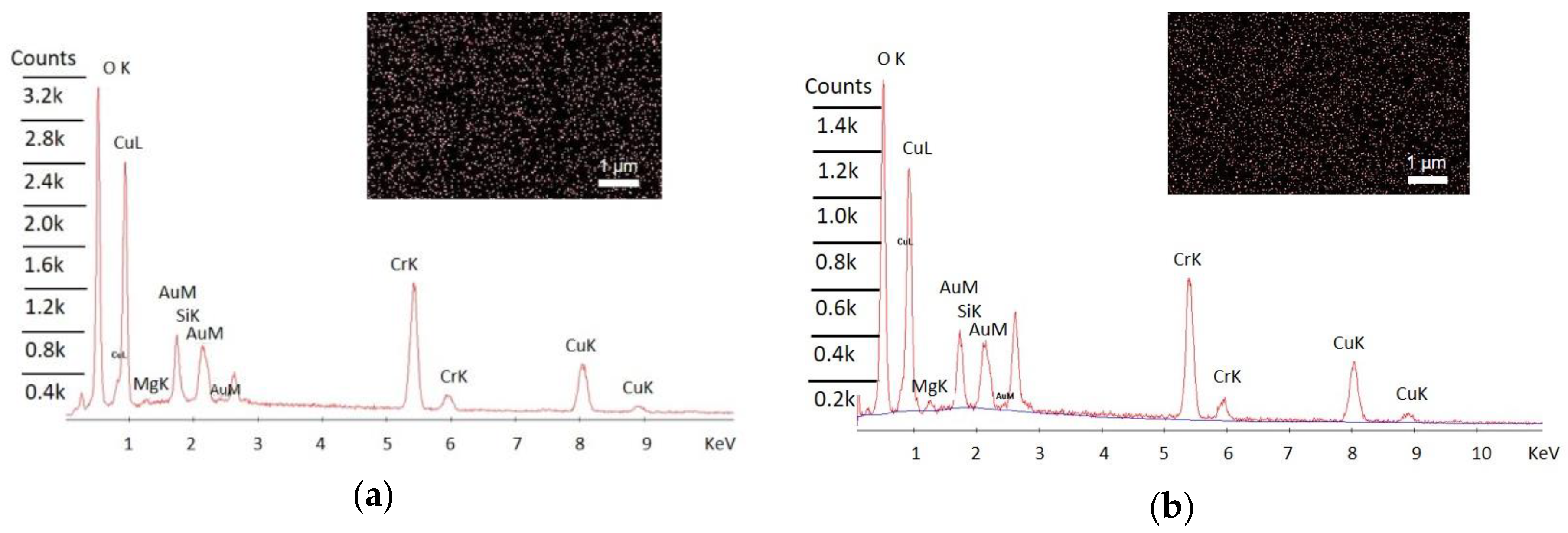
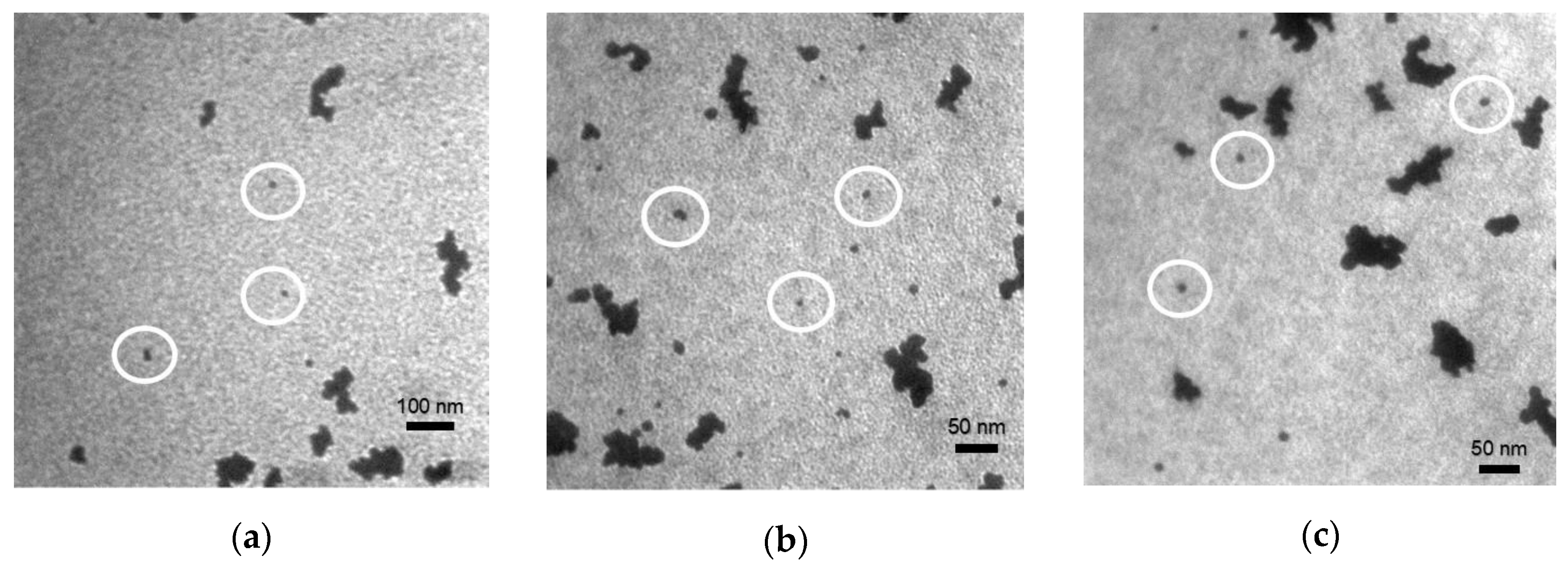
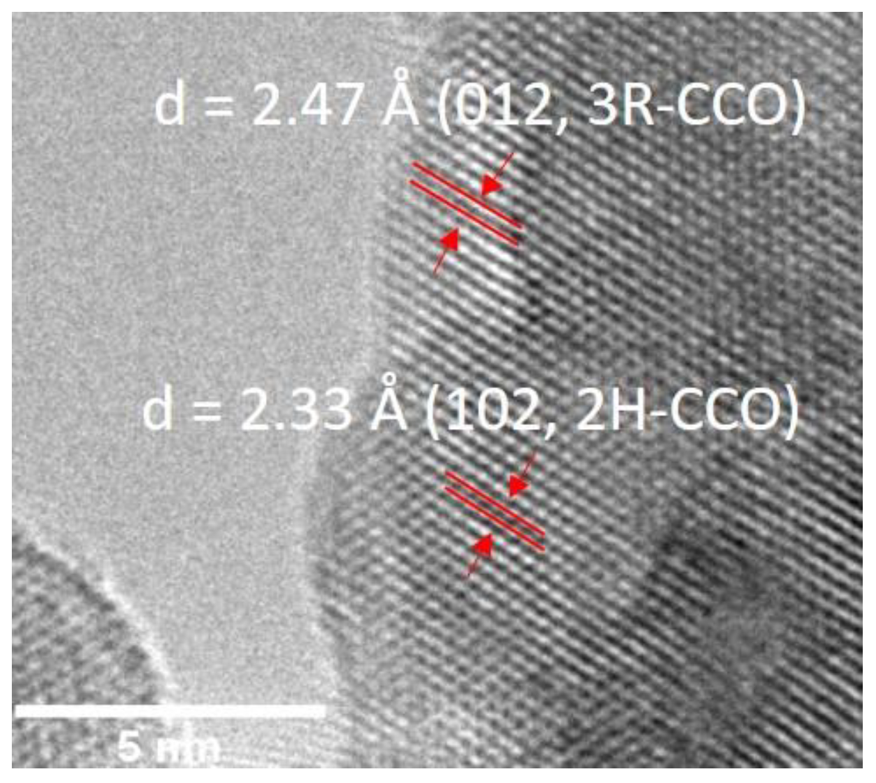
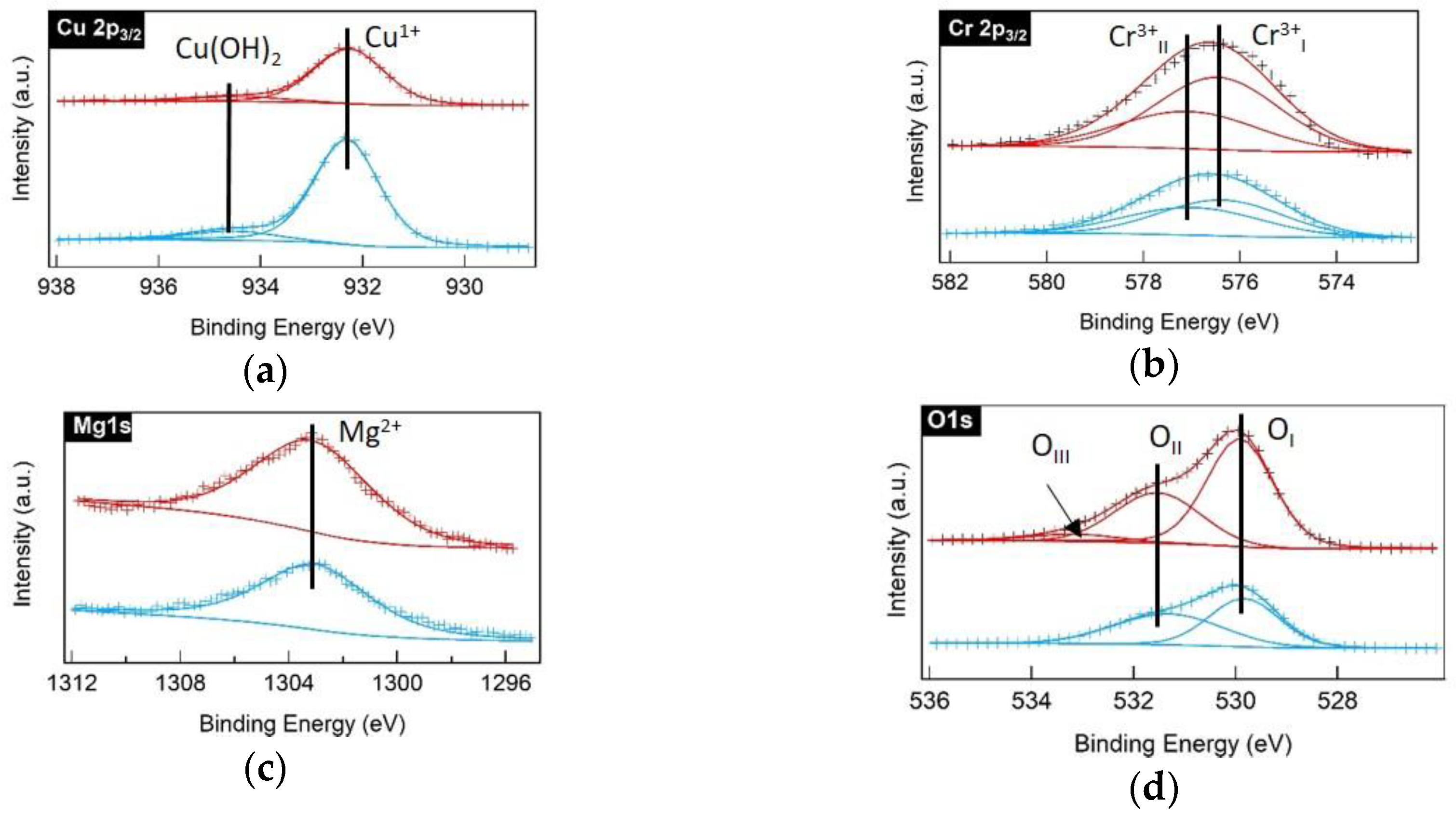
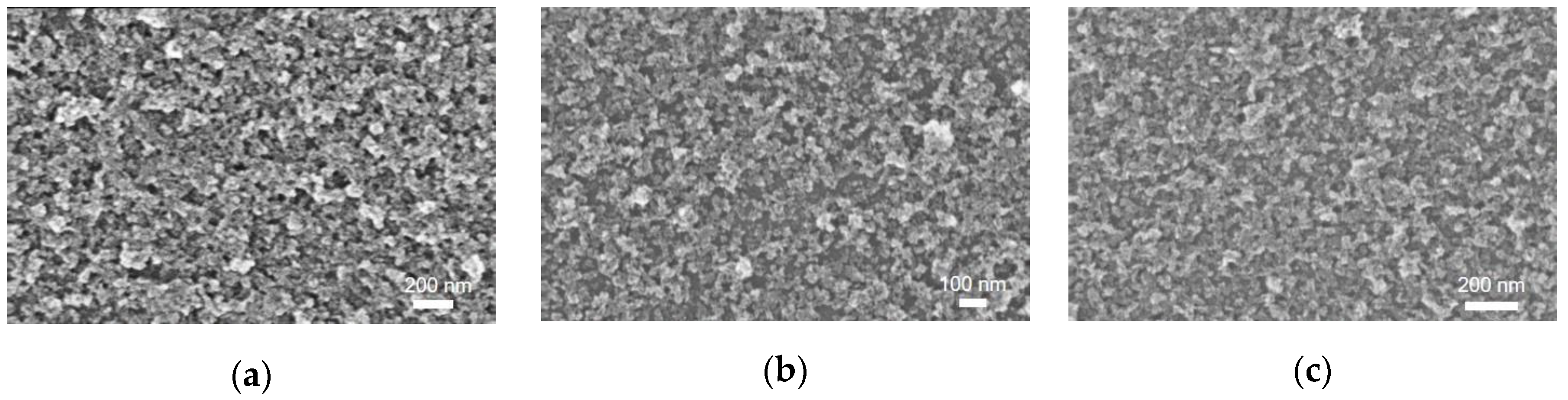
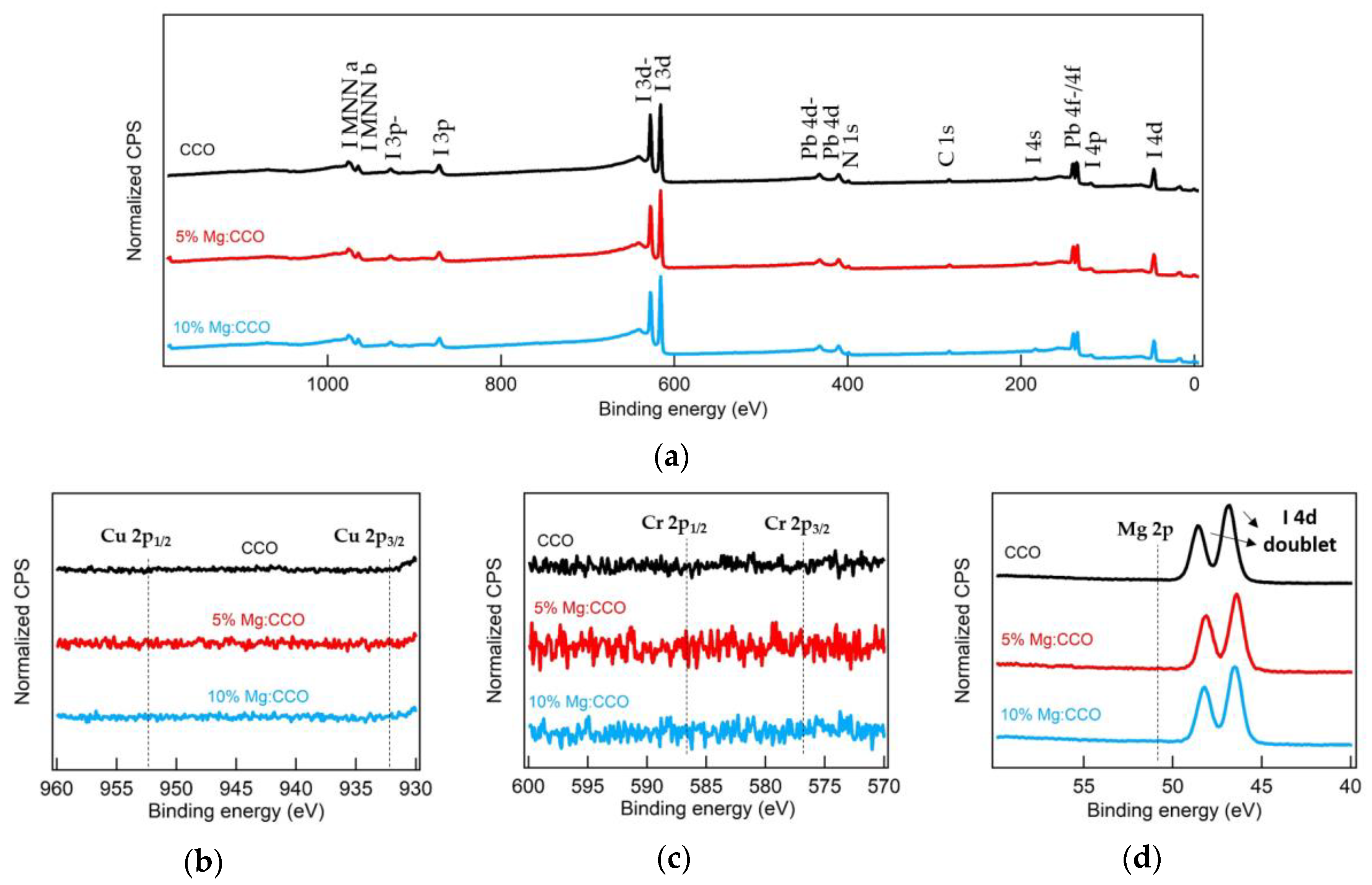
3.1. Structural, Compositional, and Morphological Characterizations

Figure 1a shows XRD patterns of CCO (black curve), 5% Mg:CCO (red curve), and 10% Mg:CCO (blue curve) powders, respectively. XRD peaks are indexed as a mixture of two CCO polytypes, rhombohedral R3m (3R-CCO, pink sticks), and hexagonal P63/mmc (2H-CCO, purple sticks), for all three compounds. No impurity phases are detected. For the (110) reflection at ~62.0°, Mg doping results in a ~0.05° peak shift to the lower angle, indicating a larger lattice spacing. The (004) reflection at 31.4° exhibits broadening with Mg doping, indicating decreased crystal size along the c axis (Figure 1a and Table 1). Rietveld refinement was carried out in order to quantitatively determine the polytype composition, crystal size, and lattice parameters for each XRD pattern. Figure 1b shows the experimental (blue solid circle), calculated (red curve), and difference between experimental and calculated (grey curve) patterns for CCO, 5% Mg:CCO, and 10% Mg:CCO. Table 1 shows the results extracted from the Rietveld refinement. The polytype compositions for all three compounds are found to be ~60 ± 3% for 3R and ~40 ± 3% for 2H. The crystal sizes decrease monotonically from CCO to 10% Mg:CCO, from 7.8 to 4.5 nm for the 2H polytype calculated from the (004) reflection and from 9.6 to 8.7 nm for the 3R polytype calculated from the (110) reflection. However, the crystal size increases monotonically from 10.2 nm for CCO to 13.1 nm for 10% Mg:CCO in the (110) reflection for the 2H polytype. The tradeoff of the size changes for both polytypes leads to similar widths of the (110) reflection independent of Mg doping. Since delafossite nanocrystals often exhibit anisotropic morphology [25,27], it is reasonable that size changes differ for the (004) and (110) reflections. Similar orientation dependent size variation in Mg:CCO was reported by Bywalez et al. [35]. They attributed the decrease of crystal sizes along the c axis to Mg2+ obstructing growth of the delafossite crystal structure and stabilizing the spinel phase. However, there is no indication that this phase exists in our samples.
The lattice parameters for 3R-CCO and 2H–CCO polytypes were similar for CCO and 5% Mg:CCO. However, for 10% Mg:CCO, a larger a lattice parameter in both phases (3.00 Å versus 2.99 Å) and an increase in the c lattice parameter in the 2H–CCO phase (11.46 Å versus 11.43 Å) were observed. This lattice expansion was consistent with Mg substituting on the Cr site, rather than the Cu site [36], because the ionic radius of Mg2+ (0.72 Å) is larger than that of Cr3+ (0.62 Å) and smaller than that of Cu+ (0.77 Å). This result is consistent with the bond length increase between Cr and O sites after Mg doping predicted from theoretical calculations [33].
In order to measure Mg concentration in CCO, EDX was performed on 5% Mg:CCO and 10% Mg:CCO. The insets of Figure 2a,b show that Mg is present and distributed uniformly in the Mg:CCO films. Mg/(Mg+Cr) represents the Mg concentration in the Mg:CCO films, which is calculated by atomic number effects (Z), absorption (A), and fluorescence (F) method from EDX spectra in Figure 2 [46]. Table 2 shows that the averaged Mg concentration in 5% Mg:CCO and 10% Mg:CCO measured from EDX is 4.0% and 9.8%, respectively. A possible Mg doping process is proposed similarly to the CCO formation mechanism as described by Miclau et al. [47]. During the hydrothermal synthesis of Mg:CCO nanoparticles, Cu1+, Cr3+, and Mg2+ ions can form Cu ( OH ) 2 , Cr ( OH ) 4 , and Mg(OH)2, respectively, at alkaline pH environment according to equations (1-3) below. Mg:CCO nanoparticles can then be formed from the metal hydroxides according to Equation (4) [48,49,50].The formation process of Mg:CCO nanoparticles are given in the following equations:
Cu 1 + + 2 H 2 O Cu ( OH ) 2 + 2 H +
Cr 3 + + 4 H 2 O Cr ( OH ) 4 + 4 H +
Mg 2 + + 2 OH   Mg ( OH ) 2
Cu ( OH ) 2 + ( 1 x ) · Cr ( OH ) 4 + x · Mg ( OH ) 2 + 2 H + CuCr 1 x Mg x O 2 + 4 H 2 O 2 x · ( OH )
TEM images of CCO (Figure 3a), 5% Mg:CCO (Figure 3b), and 10% Mg:CCO (Figure 3c) show the nanoparticles exist in individual or small clusters as well as large agglomerates. We only use individual or double nanoparticles (indicated by white circles) to determine particle sizes. The average nanoparticle size for CCO, 5% Mg:CCO, and 10% Mg:CCO is 10.3 ± 2.1, 8.2 ± 2.1, and 9.8 ± 3.0 nm, respectively. The size trend according to TEM results differs slightly from that of Rietveld-refined XRD data. One difference is that the particle size determined from XRD is analyzed for specific reflection and polytype (Table 1), while TEM images are two-dimensional projections of nanoparticles with random orientation. To examine the TEM size results in details, Figure 4a shows box plots of TEM particle sizes for CCO (black), 5% Mg:CCO (red), and 10% Mg:CCO (blue) nanoparticles. The ranges of CCO and 5% Mg:CCO nanoparticle sizes are smaller than that of 10% Mg:CCO nanoparticles. It is clear that 90% of the CCO nanoparticles are larger than 8 nm. In contrast, significant fractions of both types of Mg:CCO nanoparticles are between 6 and 8 nm. Thus, the statistics of TEM results show that Mg:CCO samples have greater numbers of smaller-sized particles, although 10% Mg doping appears to broaden the distribution. Considering the particle size results from XRD and TEM, overall Mg doping decreases CCO nanoparticle sizes because the XRD results show the size decreases along the c axis and TEM results show greater numbers of smaller sized Mg:CCO particles.
Figure 4b shows box plots of DLS sizes for CCO (black), 5% Mg:CCO (red), and 10% Mg:CCO (blue) nanoparticles dispersed in 2-MOE. For all nanoparticles, the 25–75% distributions are between 20 to 30 nm, indicating nanoparticles disperse well in 2-MOE. There are no significant differences among the three doping concentrations due to possibly similar hydrodynamic layer thickness. This is expected because the hydrodynamic layer is determined by solution ionic strength and hydrodynamic size and is often larger than dry particle size [51,52]. Since the Mg concentration in these nanoparticles is low, it is not surprising that hydrodynamic sizes for all samples are similar.
The HR TEM image of 5% Mg:CCO nanoparticles shows clear lattice fringes (Figure 5). The lattice spacing of 2.47 Å corresponds to the (012) reflection for 3R–CCO polytype. The lattice spacing of 2.33 Å corresponds to the (102) reflection for 2H–CCO polytype. No other lattice spacings corresponding to impurity phases are detected, consistent with XRD results.
XPS studies were carried out in order to confirm the oxidation states of Cu, Cr, and Mg in the Mg:CCO powders. XPS data was analyzed using PHI Multipak software and peak fitting was done using a Gaussian–Lorentzian profile after a Shirley type background subtraction [53]. The binding energy was shifted using the valence band edge. The measured (cross symbol) and fitted (solid curve) XPS spectra of Cu 2p3/2, Cr 2p3/2, Mg 1s, and O 1s core levels for 5% Mg:CCO (red color) and 10% Mg:CCO (blue color) nanoparticles are shown in Figure 6. Deconvolution of the Cu 2p3/2 spectrum for both 5% and 10% Mg:CCO (Figure 6a) results in two peaks at 934.6 eV and 932.3 eV corresponding to binding energies of Cu(OH)2 and Cu1+, respectively, consistent with the literature [54,55]. The Cr 2p3/2 spectrum (Figure 6b) can be fitted to two peaks at 577.3 eV and 576.5 eV corresponding to binding energies of Cr3+ as hydroxide and Cr3+ as oxide, respectively [37,56]. These are similar to the binding energy peak positions of Cu1+ and Cr3+ oxide of undoped CCO nanoparticles reported in the literature [24]. Figure 6c shows the Mg 1s spectra, wherein the peak is located at binding energy of 1303.1 eV, corresponding to the Mg2+ oxidation state [39]. The O 1s spectrum (Figure 6d) shows peaks corresponding to lattice oxygen (OI) at 529.9 eV and hydroxyl groups (OII) at 531.5 eV for both 5% Mg:CCO and 10% Mg:CCO nanoparticles. A small-intensity peak at 533 eV corresponding to adsorbed water for 5% Mg:CCO nanoparticles is observed [54,57].

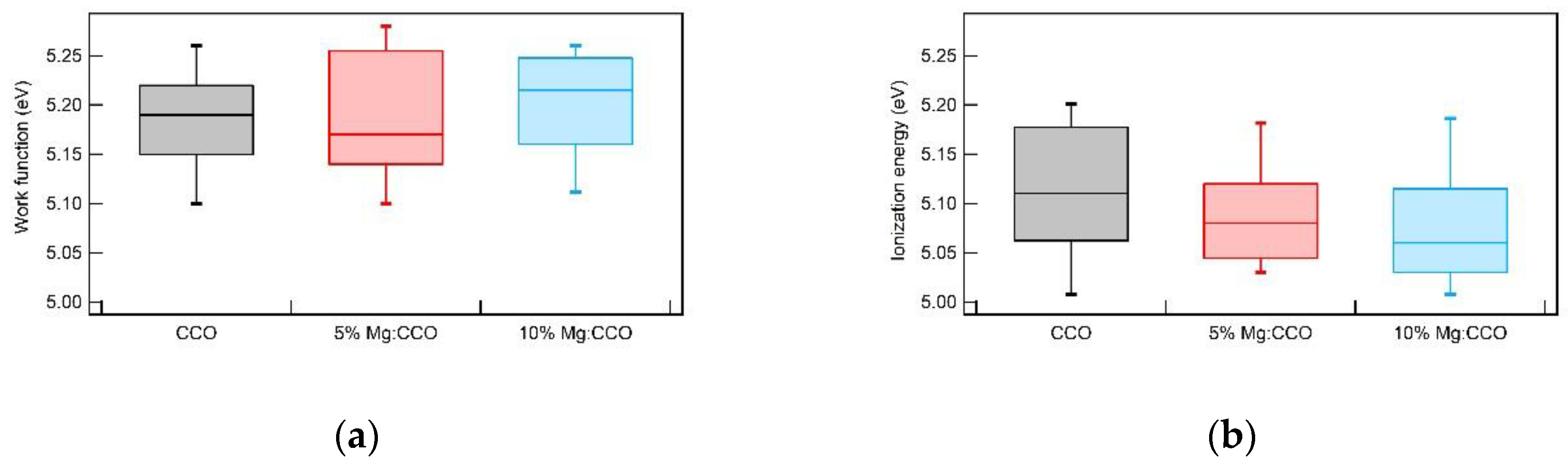
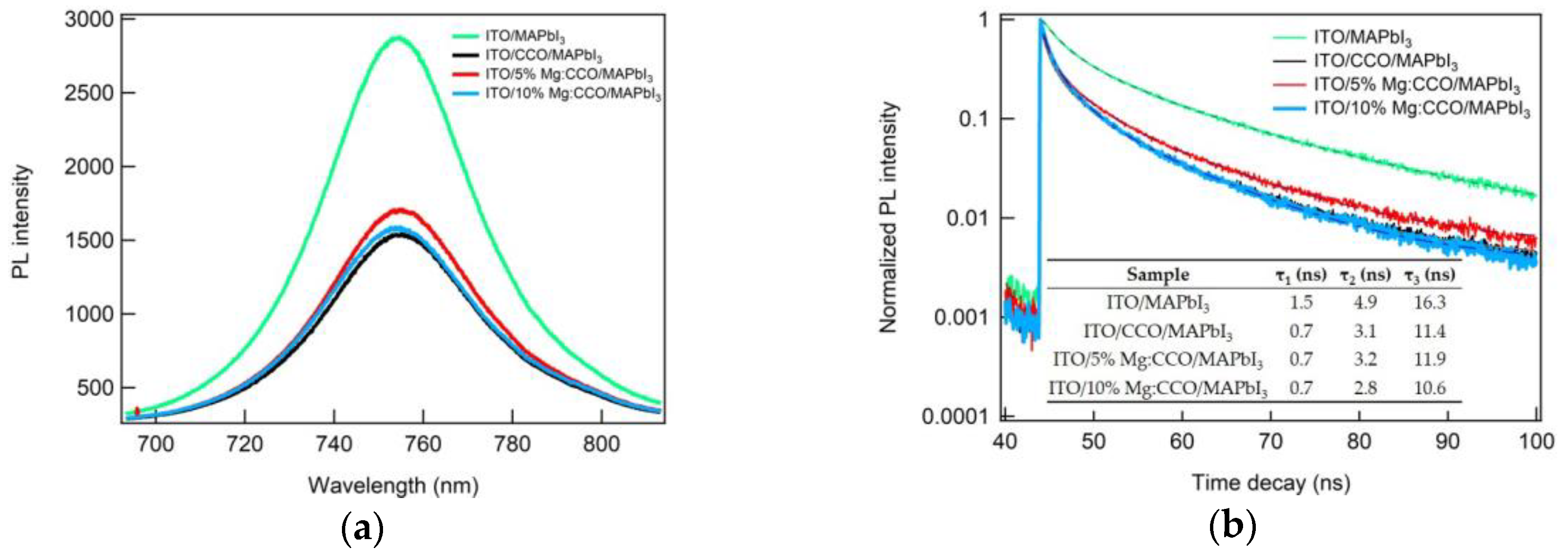
3.2. Optical and Electronic Characterizations

The thickness of CCO and Mg:CCO nanoparticle films are controlled by the number of coating cycles that were performed during deposition [27]. Figure 7a–c shows SEM images for CCO, 5% Mg:CCO, and 10% Mg:CCO films; no regions of bare substrate are seen for all films. Figure 8a shows the UV-vis absorbance and transmission (inset) spectra of well-covered CCO (black), 5% Mg:CCO (red), and 10% Mg:CCO (blue) films. The absorbance values at 300 nm lie between 0.21 and 0.22 for all films, which are highly transparent (transmission > 90%) in the visible region. All three films are 18 nm thick as determined by ellipsometry. The direct band gap (Eg) is extrapolated from the Tauc plot (Figure 8b). The average values of the direct Eg are 3.27 ± 0.02 eV, 3.25 ± 0.03 eV, and 3.27 ± 0.03 eV for CCO, 5% Mg:CCO, and 10% Mg:CCO, respectively (Table 3). These values are the same within the uncertainty of the measurement (~0.03 eV). Thus, Mg doping does not affect the direct Eg of CCO. The Eg for pure CCO is consistent with our previous result [27].
Figure 9a shows box plots of the work function (WF) for CCO (black), 5% Mg:CCO (red), and 10% Mg:CCO (blue) films. The median WF values of CCO, 5% Mg:CCO, and 10% Mg:CCO films are 5.19, 5.17, and 5.22 eV, respectively. The 50th percentile WF value for the 10% Mg:CCO is higher than that of CCO and 5% Mg:CCO. The 5% Mg:CCO films exhibit the largest spread with a long tail to the large WF than CCO films. Thus, Mg:CCO films generally appear to have higher WF values than CCO films, although the difference is below the level of statistical significance. Figure 9b shows box plots of the ionization energy (IE) for CCO (black), 5% Mg:CCO (red), and 10% Mg:CCO (blue) films. The median IE values of CCO, 5% Mg:CCO, and 10% Mg:CCO films are 5.11, 5.08, and 5.06 eV, respectively. The energy step for the IE measurement is 0.05 eV. The 50-percentile IE value decreases monotonically with increasing Mg concentration. Furthermore, the measured IE value is consistent with the IE of 5.1 eV from previous band structure calculations [27]. As shown in Figure 9, the overall WF values are larger than IE values, especially for Mg:CCO films. Thus, these films are p-type degenerately doped. The difference between WF and IE values (WF – IE) increases with Mg concentration from 0.08 eV for CCO to 0.16 eV for 10% Mg:CCO (Table 3), indicating that Mg:CCO films may have higher conductivity, consistent with previous results [35,36].

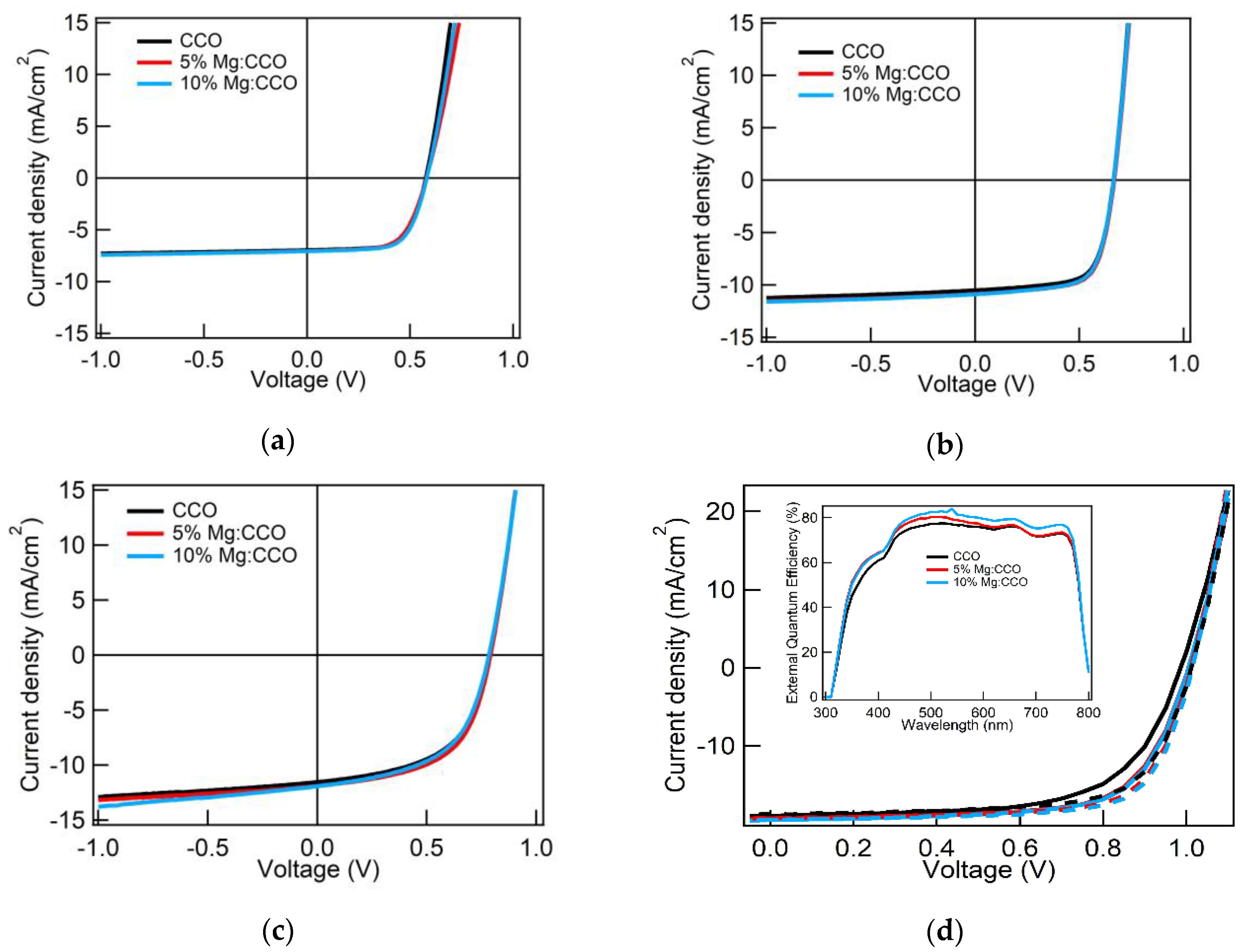
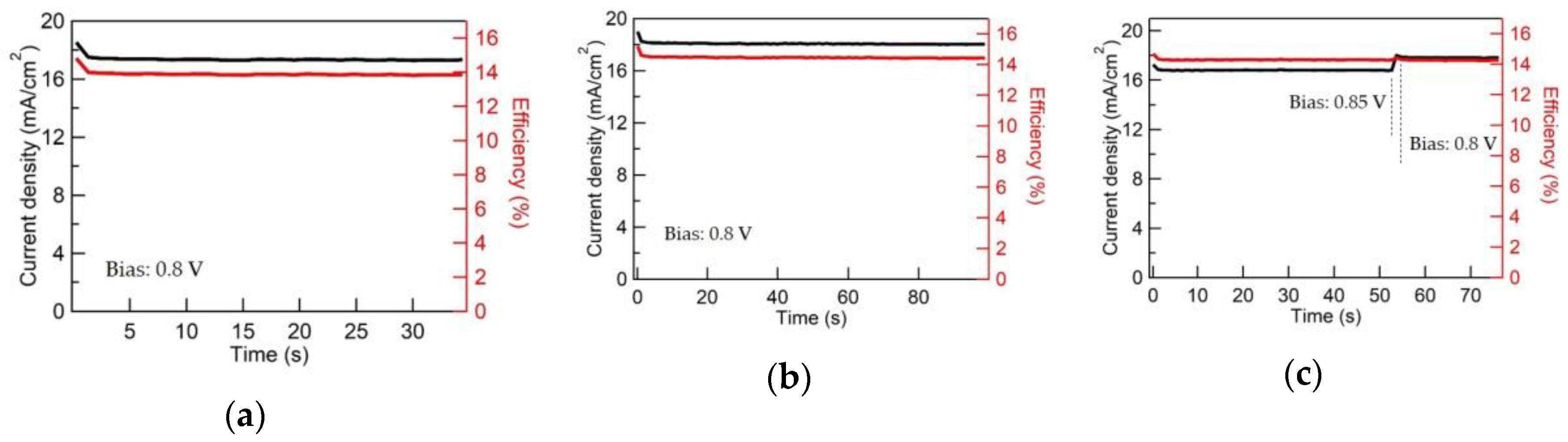
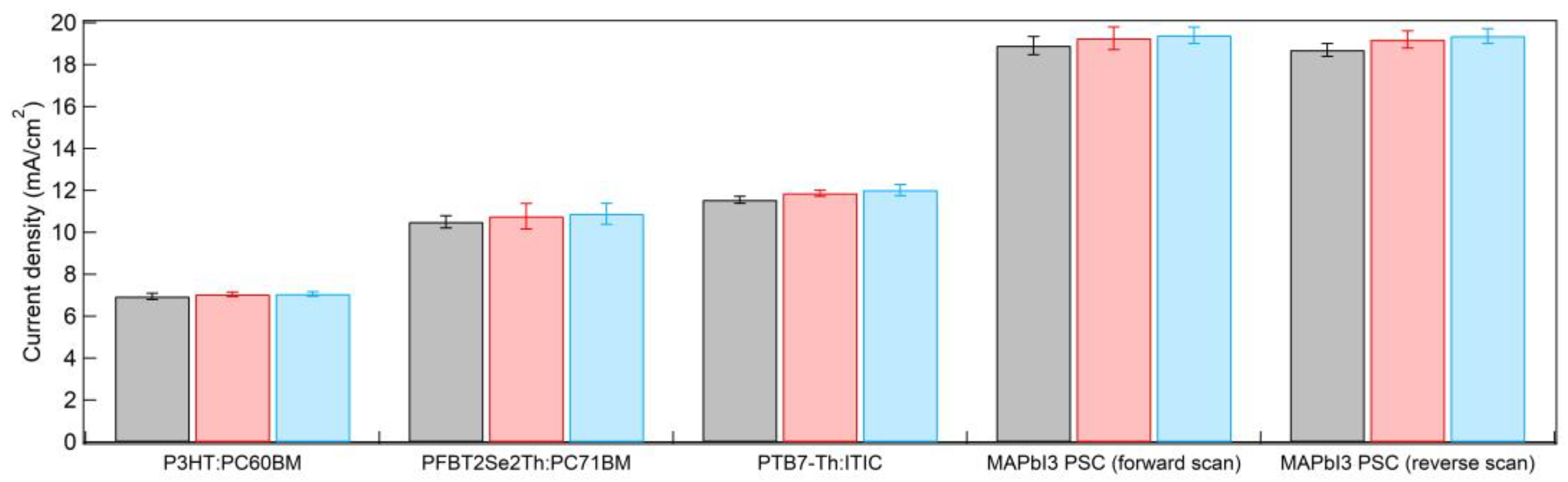
3.3. CCO and Mg:CCO as HTLs in OSCs and PSCs

Figure 10a and Table 4 show the results of P3HT:PC61BM devices with CCO (black), 5% Mg:CCO (red), and 10% Mg:CCO (blue) HTLs. The average Jsc of P3HT:PC61BM devices is higher with Mg:CCO HTL (from 6.94 mA cm−2 for CCO to ~7.05 mA cm−2 for Mg:CCO). The average Voc of Mg:CCO is also higher than that of undoped CCO HTL (~0.582 V versus 0.570 V). However, both Mg:CCO devices exhibit lower average FF (0.642 for 5% doping and 0.666 for 10% doping versus 0.685 for no doping). The tradeoff of the three parameters leads to similar PCE values for all devices independent of Mg doping. We note that the variation among different diodes is larger in Jsc than Voc or FF, which is typical of OPV devices. Nonetheless, there is a systematic trend of average Jsc increase with Mg doping.
Figure 10b and Table 4 show the results of PFBT2Se2Th:PC71BM devices with CCO (black), 5% Mg:CCO (red), and 10% Mg:CCO (blue) HTLs. The average Voc and FF are similar in all devices with values of ~0.665 V and ~0.685, respectively. The average Jsc of the devices increases monotonically from 10.50 mA cm−2 for undoped CCO HTL to 10.88 mA cm−2 for 10% Mg:CCO HTL. Thus, the PCE values of PFBT2Se2Th:PC71BM devices are higher when Mg:CCO, instead of undoped CCO, is used as the HTL. Among different diodes, the variation of Jsc is larger than that of Voc or FF. Moreover, Mg:CCO devices have even larger variation of Jsc. However, a similar systematic trend of increasing average Jsc as P3HT:PC61BM devices is observed in PFBT2Se2Th:PC71BM devices.
Figure 10c and Table 4 show the results of PTB7-Th:ITIC devices with CCO (black), 5% Mg:CCO (red), and 10% Mg:CCO (blue) HTLs. The average Jsc of the devices increases monotonically from 11.55 mA cm−2 for undoped CCO HTL to 12.02 mA cm−2 for 10% Mg:CCO HTL. The average Voc and FF are highest for the 5% Mg:CCO in this batch of devices, but they do not depend on Mg doping in other batches. Generally, the PCE values of PTB7-Th:ITIC devices are higher when using Mg:CCO as the HTL due to the increase in Jsc. This work is the first using CCO and Mg:CCO as HTL for BHJ OSCs with a non-fullerene acceptor.
Figure 10d and Table 4 show the results of MAPbI3 PSCs with CCO (black), 5% Mg:CCO (red), and 10% Mg:CCO (blue) HTLs under forward (solid lines) and reverse scans (dashed lines). Only slight hysteresis is seen, indicating minimal trap states at the CCO or Mg:CCO/perovskite interface. Under forward scan, the average Voc increases monotonically from 0.985 V for the undoped CCO HTL to 1.007 V for the 10% Mg:CCO HTL. Similar trends are observed in the Jsc (from 18.91 mA cm−2 for the undoped CCO HTL to 19.40 mA cm−2 for the 10% Mg:CCO HTL) and FF (from 0.678 for the undoped CCO HTL to 0.703 for the 10% Mg:CCO HTL). Overall, the PCE of the devices improves monotonically from 12.64% for the undoped CCO HTL to 13.73% for the 10% Mg:CCO HTL. We note that the variation among different diodes is large for all the parameters. However, there are systematic trends of increases among the average Jsc, Voc, and FF with Mg doping. Under reverse scan, the average Jsc increases monotonically from 18.70 mA cm−2 for the undoped CCO HTL to 19.37 mA cm−2 for the 10% Mg:CCO HTL. The FF of the devices using the 5% Mg:CCO and 10% Mg:CCO HTLs were similar, 0.719, but for the undoped CCO HTL, a lower FF (0.697 versus 0.719) was observed. The Voc is similar in all devices with values of ~1.01 V. Overall, the PCE of the devices improves monotonically from 13.19% for the undoped CCO HTL to 14.12% for the 10% Mg:CCO HTL. As in the forward scan data, despite the variation among different diodes, there is a systematic trend of increasing average Jsc with Mg doping. Jeong et al. observed that Mg:CCO produces PSCs with a slightly higher Jsc and Voc, but a lower FF, resulting in no improvement in the PCE; however, they did not report Mg concentration [40]. The inset in Figure 8d shows the external quantum efficiency (EQE) at wavelength ranging from 300 to 800 nm for CCO (black), 5% Mg:CCO (red), and 10% Mg:CCO (blue) HTLs. A broadband increase in EQE is observed with Mg doping, consistent with the increases of average Jsc in forward and reverse J-V scans.
Several groups have reported elemental diffusion from inorganic transport layer into MAPbI3 when using CdS ETL [58], CrOx [59], and CuI [60] HTLs. In order to examine this possibility, we performed XPS studies on the surfaces of MAPbI3 films on top of ITO/HTL. Figure 11 shows the normalized XPS spectra of (a) survey, (b) Cu 2p, (c) Cr 2p, and (d) Mg 2p core levels for MAPbI3 films processed on top of CCO (black), 5% Mg:CCO (red), and 10% Mg:CCO (blue) HTLs. For all HTLs, all peaks in the survey spectra are indexed as the component elements (C, N, Pb, and I) of MAPbI3, consistent with our previous result [27]. The Cu 2p and Cr 2p spectral ranges are free of any peaks corresponding to Cu 2p or Cr 2p (dashed lines), indicating no presence of Cu and Cr elements at the surface of MAPbI3 layer. The Mg 2p spectrum shows two peaks at 48.2 eV and 46.6 eV corresponding to the binding energy of the I 4d orbitals [61]. No Mg 2p peak at 50.8 eV (dashed line) was detected, indicating no presence of Mg element. Thus, if metal diffusion from CCO and Mg:CCO HTLs into MAPbI3 occurs, it does so at a level below the sensitivity of XPS. This result is consistent with thermodynamic calculation: the calculated formation enthalpy of CCO is -6.0 eV [22], significantly lower compared to that of CdS (−1.5 eV) [62] and CuI (−0.3 eV) [63] and slightly lower compared to that of Cr2O3 (−5.9 eV) [64]. Mg:CCO has the same crystalline structure as CCO and the Mg doping content is small, thus, the formation enthalpy of Mg:CCO is expected to be similar to that of CCO. Thus, CCO and Mg:CCO are more stable and less likely to decompose or react than the aforementioned HTLs. Nevertheless, additional experimentation is warranted to explore the possibility of reactivity between CCO/Mg:CCO and perovskite phases.
In order to explore charge transport at the CCO and Mg:CCO/MAPbI3 interface, we performed TRPL measurements. Figure 12a shows the PL emission spectrum for ITO/MAPbI3 (green), ITO/CCO/MAPbI3 (black), ITO/5% Mg:CCO/MAPbI3 (red), and ITO/10% Mg:CCO/MAPbI3 (blue). For all samples, the main PL emission peaks are at ~750 nm, consistent with the literature [66]. PL intensities for MAPbI3 on top of CCO and Mg:CCO HTLs are lower compared to that of MAPbI3 on ITO, indicating CCO and Mg:CCO HTLs are effective in promoting charge transfer. However, PL intensities are similar among MAPbI3 on top of CCO and Mg:CCO HTLs. Figure 12b shows the normalized TRPL decay kinetics for ITO/MAPbI3 (green), ITO/CCO/MAPbI3 (black), ITO/5% Mg:CCO/MAPbI3 (red), and ITO/10% Mg:CCO/MAPbI3 (blue). With the addition of CCO and Mg:CCO HTLs, a faster PL decay is observed relative to ITO/MAPbI3. The inset table in Figure 12b shows the PL lifetimes extracted from three exponential fits in all samples (lines in Figure 12b). The τ1, τ2, and τ3 lifetimes of the ITO/MAPbI3 structure are 1.5 ns, 4.9 ns, and 16.3 ns, respectively. After adding CCO and Mg:CCO HTLs, the τ1, τ2, and τ3 decreases to 0.7 ns, ~3.0 ns, and ~11.0 ns, respectively, indicating enhanced charge extraction and consistent with the literature result [66]. Again, there are no significant differences in PL lifetimes among films of MAPbI3 on CCO and Mg:CCO HTLs. Mg doping in CCO is expected to lead lower PL intensity and shorter lifetimes. However, these effects are not discernable in our TRPL results, presumably because they may be confounded by factors besides charge transfer, such as surface recombination [67].
Figure 13 shows the stabilized photocurrents and efficiencies for representative MAPbI3 cells with CCO, 5% Mg:CCO, and 10% Mg:CCO HTLs. Time-dependent photocurrent measurements are taken at a bias of ~0.8 V with stabilized photocurrent values of 17.35 mA cm−2, 18.05 mA cm−2, and 17.81 mA cm−2 for CCO, 5% Mg:CCO, and 10% Mg:CCO HTLs, respectively. The values of the stabilized photocurrent are higher with Mg doping, reflecting the increases in Jsc and FF observed in forward and reverse scans for Mg:CCO MAPbI3 PSCs. The stabilized efficiencies for CCO, 5% Mg:CCO, and 10% Mg:CCO HTLs are 13.89%, 14.43%, and 14.26%, respectively.
Figure 14 shows the bar charts of average Jsc for P3HT:PC61BM OSCs, PFBT2Se2Th:PC71BM OSCs, PTB7-Th:ITIC OSCs, and MAPbI3 PSCs under forward and reverse scans for CCO (black color), 5% Mg:CCO (red color), and 10% Mg:CCO (blue color) HTLs. The average Jsc of all OSCs and MAPbI3 PSCs are higher with Mg:CCO HTLs. The small average Jsc increases in all systems may be partially attributed to the better conductivity of Mg:CCO HTLs resulting from the increased WF with respect to IE with Mg doping. Additionally, the broadband increase with Mg doping content in the EQE spectra of PSCs (Figure 10d inset) signifies that the increased HTL work function contributes to a stronger electric field within the device, more efficiently extracting photoexcited carriers regardless of the depth at which the generating photons are absorbed. If Voc and FF are independent of Mg doping, the PCE may be expected to increase due to the boost in Jsc. However, they do not show a consistent trend from batch to batch. Voc and FF are more susceptible to film roughness, which can vary due to aggregation of the nanoparticles in the suspensions and variation in spin coating conditions. The tradeoff between Jsc and Voc/FF results in little or no statistical PCE improvement (Table 4).

4. Conclusions

In summary, we synthesized CCO and Mg:CCO nanoparticles and successfully applied them as HTLs in OSCs and PSCs. Mg incorporation induces a slight lattice expansion by substituting larger ionic radii Mg2+ into the Cr3+ site. Rietveld refinement suggests that Mg doping decreases CCO nanoparticle size along the c axis but increases CCO nanoparticle size along the in-plane directions. Overall, both XRD and TEM results indicate that nanoparticle sizes are smaller with Mg doping. The average value of the direct Eg is (3.26 ± 0.03) eV in all nanoparticle films. The WF values for all Mg concentrations are larger than the IE values, and their difference (WF – IE) increases with Mg concentration, consistent with increased p-type conductivity reported in the literature. OSCs and PSCs based on Mg:CCO HTLs show a consistent increase in average Jsc in all four absorber systems despite large uncertainties; however, an overall enhancement in PCE is not clearly discernible (except in PSCs) due to different trends in other parameters and sample variation. No elemental (Cu, Cr, and Mg) diffusion from CCO and Mg:CCO HTLs is detected by XPS at the surface of MAPbI3 films. CCO and Mg:CCO HTLs effectively extract charge from the absorber, as evident in more PL quenching and shorter lifetimes when MAPbI3 is deposited on the HTLs. Mg doping in CCO HTLs enhances the stabilized efficiency for MAPbI3 PSCs. This work provides new insights related to the role that an Mg:CCO HTL may play in improving performance in a wide range of OSCs and MAPbI3 PSCs.

Author Contributions

Conceptualization, J.W.P.H.; Nanoparticle synthesis, making suspensions and thin films, XRD, SEM, EDX, DLS, UV-vis, PESA, Kelvin Probe, ellipsometry, B.Z.; TEM, XRD, XPS analyses, S.T. and B.Z.; OSC fabrication and PL sample preparation, B.Z. and W.X.; PSC fabrication and XPS, W.A.D.-S. and D.B.M.; Se polymer synthesis, F.-Y.C. and Y.-J.C.; PL quenching measurements and analyses, Y.Z. and A.V.M.; writing—original draft preparation, B.Z.; writing—review and editing, S.T., J.W.P.H., W.A.D.-S., and D.B.M.

Funding

The work done at University of Texas at Dallas (J.W.P.H., B.Z., W.X., S.T.) was sponsored by the National Science Foundation (NSF) (Grant No. DMR-1305893). PL spectroscopy work (Y.Z. and A.V.M.) was supported by NSF-CAREER grant #1350800. J.W.P.H. acknowledges the support from Texas Instruments Distinguished Chair in Nanoelectronics. The work done at Duke University was funded by the Office of Energy Efficiency and Renewable Energy (EERE), U.S. Department of Energy, under Award Number DE-EE0006712 (W.A.D.-S., D.B.M.). W.A.D.-S. acknowledges support from the Fitzpatrick Institute for Photonics John T. Chambers Scholarship.

Acknowledgments

We thank Trey Daunis for review and editing this manuscript and Ivanic Bojana for the help of PL quenching measurements.

Conflicts of Interest

The authors declare no conflict of interest.

References

  1. Jung, E.H.; Jeon, N.J.; Park, E.Y.; Moon, C.S.; Shin, T.J.; Yang, T.-Y.; Noh, J.H.; Seo, J. Efficient, stable and scalable perovskite solar cells using poly(3-hexylthiophene). Nature 2019, 567, 511–515. [Google Scholar] [CrossRef]
  2. Cui, Y.; Yao, H.; Zhang, J.; Zhang, T.; Wang, Y.; Hong, L.; Xian, K.; Xu, B.; Zhang, S.; Peng, J.; et al. Over 16% efficiency organic photovoltaic cells enabled by a chlorinated acceptor with increased open-circuit voltages. Nat. Commun. 2019, 10, 2515. [Google Scholar] [CrossRef] [PubMed]
  3. Hany, R.; Lin, H.; Castro, F.A. Focus issue on organic and hybrid photovoltaics. Sci. Technol. Adv. Mater. 2019, 20, 42–43. [Google Scholar] [CrossRef] [PubMed] [Green Version]
  4. Yip, H.-L.; Jen, A.K.-Y. Recent advances in solution-processed interfacial materials for efficient and stable polymer solar cells. Energy Environ. Sci. 2012, 5, 5994–6011. [Google Scholar] [CrossRef]
  5. Yan, C.; Barlow, S.; Wang, Z.; Yan, H.; Jen, A.K.-Y.; Marder, S.R.; Zhan, X. Non-fullerene acceptors for organic solar cells. Nat. Rev. Mater. 2018, 3, 18003. [Google Scholar] [CrossRef]
  6. Teh, C.H.; Daik, R.; Lim, E.L.; Yap, C.C.; Ibrahim, M.A.; Ludin, N.A.; Sopian, K.; Teridi, M.A.M. A review of organic small molecule-based hole-transporting materials for meso-structured organic–inorganic perovskite solar cells. J. Mater. Chem. A 2016, 4, 15788–15822. [Google Scholar] [CrossRef]
  7. Su, Y.W.; Lan, S.C.; Wei, K.H. Organic photovoltaics. Mater. Today 2012, 15, 554–562. [Google Scholar] [CrossRef]
  8. Liu, J.; Wu, Y.; Qin, C.; Yang, X.; Yasuda, T.; Islam, A.; Zhang, K.; Peng, W.; Chen, W.; Han, L. A dopant-free hole-transporting material for efficient and stable perovskite solar cells. Energy Environ. Sci. 2014, 7, 2963–2967. [Google Scholar] [CrossRef]
  9. Kawano, K.; Pacios, R.; Poplavskyy, D.; Nelson, J.; Durrant, J.R. Degradation of organic solar cells due to air exposure. Sol. Energy Mater. Sol. Cells 2006, 90, 3520–3530. [Google Scholar] [CrossRef]
  10. You, J.; Meng, L.; Song, T.-B.; Guo, T.-F.; Yang, Y.; Chang, W.-H.; Hong, Z.; Chen, H.; Zhou, H.; Chen, Q.; et al. Improved air stability of perovskite solar cells via solution-processed metal oxide transport layers. Nat. Nanotechnol. 2016, 11, 75–81. [Google Scholar] [CrossRef]
  11. Stubhan, T.; Li, N.; Luechinger, N.A.; Halim, S.C.; Matt, G.J.; Brabec, C.J. High Fill Factor Polymer Solar Cells Incorporating a Low Temperature Solution Processed WO3 Hole Extraction Layer. Adv. Energy Mater. 2012, 2, 1433–1438. [Google Scholar] [CrossRef]
  12. Lee, Y.-J.; Yi, J.; Gao, G.F.; Koerner, H.; Park, K.; Wang, J.; Luo, K.; Vaia, R.A.; Hsu, J.W.P. Low-temperature solution-processed molybdenum oxide nanoparticle hole transport layers for organic photovoltaic devices. Adv. Energy Mater. 2012, 2, 1193–1197. [Google Scholar] [CrossRef]
  13. Wang, J.; Xu, L.; Lee, Y.-J.; Villa, M.D.A.; Malko, A.V.; Hsu, J.W.P. Effects of Contact-Induced Doping on the Behaviors of Organic Photovoltaic Devices. Nano Lett. 2015, 15, 7627–7632. [Google Scholar] [CrossRef] [PubMed]
  14. Hammond, S.R.; Meyer, J.; Widjonarko, N.E.; Ndione, P.F.; Sigdel, A.K.; Miedaner, A.; Lloyd, M.T.; Kahn, A.; Ginley, D.S.; Berry, J.J.; et al. Low-temperature, solution-processed molybdenum oxide hole-collection layer for organic photovoltaics. J. Mater. Chem. 2012, 22, 3249–3254. [Google Scholar] [CrossRef]
  15. Singh, R.; Singh, P.K.; Bhattacharya, B.; Rhee, H.-W. Review of current progress in inorganic hole-transport materials for perovskite solar cells. Appl. Mater. Today 2019, 14, 175–200. [Google Scholar] [CrossRef]
  16. Jiang, F.; Choy, W.C.H.; Li, X.; Cheng, J. Post-treatment-Free Solution-Processed Non-stoichiometric NiOx Nanoparticles for Efficient Hole-Transport Layers of Organic Optoelectronic Devices. Adv. Mater. 2015, 27, 2930–2937. [Google Scholar] [CrossRef] [PubMed]
  17. Hüfner, S. Electronic structure of NiO and related 3d-transition-metal compounds. Adv. Phys. 1994, 43, 183–356. [Google Scholar] [CrossRef]
  18. Renaud, A.; Chavillon, B.; Pleux, L.L.; Pellegrin, Y.; Blart, E.; Boujtita, M.; Pauporté, T.; Cario, L.; Jobic, S.; Odobel, F. CuGaO2: A promising alternative for NiO in p-type dye solar cells. J. Mater. Chem. 2012, 22, 14353–14356. [Google Scholar] [CrossRef]
  19. Kawazoe, H.; Yasukawa, M.; Hyodo, H.; Kurita, M.; Yanagi, H.; Hosono, H. P-type electrical conduction in transparent thin films of CuAlO2. Nature 1997, 389, 939–942. [Google Scholar] [CrossRef]
  20. Sheets, W.C.; Mugnier, E.; Barnabe´, A.; Marks, T.J.; Poeppelmeier, K.R. Hydrothermal Synthesis of Delafossite-Type Oxides. Chem. Mater. 2006, 18, 7–20. [Google Scholar] [CrossRef]
  21. Marquardt, M.A.; Ashmore, N.A.; Cann, D.P. Crystal chemistry and electrical properties of the delafossite structure. Thin Solid Films 2006, 496, 146–156. [Google Scholar] [CrossRef]
  22. Scanlon, D.O.; Watson, G.W. Understanding the p-type defect chemistry of CuCrO2. J. Mater. Chem. 2011, 21, 3655–3663. [Google Scholar] [CrossRef]
  23. Arnold, T.; Payne, D.J.; Bourlange, A.; Hu, J.P.; Egdell, R.G.; Piper, L.F.J.; Colakerol, A.D.M.; Glans, P.A.; Learmonth, T.; Smith, K.E.; et al. X-ray spectroscopic study of the electronic structure of. Phys. Rev. B 2009, 79, 075102. [Google Scholar] [CrossRef]
  24. Wang, J.; Lee, Y.-J.; Hsu, J.W.P. Sub-10 nm copper chromium oxide nanocrystals as a solution processed p-type hole transport layer for organic photovoltaics. J. Mater. Chem. C 2016, 4, 3607–3613. [Google Scholar] [CrossRef]
  25. Xiong, D.; Xu, Z.; Zeng, X.; Zhang, W.; Chen, W.; Xu, X.; Wang, M.; Cheng, Y.-B. Hydrothermal synthesis of ultrasmall CuCrO2 nanocrystal alternatives to NiO nanoparticles in efficient p-type dye-sensitized solar cells. J. Mater. Chem. 2012, 22, 24760–24768. [Google Scholar] [CrossRef]
  26. Zhang, H.; Wang, H.; Zhu, H.; Chueh, C.-C.; Chen, W.; Yang, S.; Jen, A.K.-Y. Low-Temperature Solution-Processed CuCrO2 Hole-Transporting Layer for Efficient and Photostable Perovskite Solar Cells. Adv. Energy Mater. 2018, 8, 1702762. [Google Scholar] [CrossRef]
  27. Dunlap-Shohl, W.A.; Daunis, T.B.; Wang, X.; Wang, J.; Zhang, B.; Barrera, D.; Yan, Y.; Hsu, J.W.P.; Mitzi, D.B. Room-temperature fabrication of a delafossite CuCrO2 hole transport layer for perovskite solar cells. J. Mater. Chem. A 2018, 6, 469–477. [Google Scholar] [CrossRef]
  28. Yang, B.; Ouyang, D.; Huang, Z.; Ren, X.; Zhang, H.; Choy, W.C.H. Multifunctional Synthesis Approach of In:CuCrO2 Nanoparticles for Hole Transport Layer in High-Performance Perovskite Solar Cells. Adv. Funct. Mater. 2019, 29, 1902600. [Google Scholar] [CrossRef]
  29. Akin, S.; Liu, Y.; Dar, M.I.; Zakeeruddin, S.M.; Grätzel, M.; Turan, S.; Sonmezoglu, S. Hydrothermally processed CuCrO2 nanoparticles as an inorganic hole transporting material for low-cost perovskite solar cells with superior stability. J. Mater. Chem. A 2018, 6, 20327–20337. [Google Scholar] [CrossRef]
  30. Zheng, S.Y.; Jiang, G.S.; Su, J.R.; Zhu, C.F. The structural and electrical property of CuCr1−xNixO2 delafossite compounds. Mater. Lett. 2006, 60, 3871–3873. [Google Scholar] [CrossRef]
  31. Nagarajan, R.; Draeseke, A.D.; Sleight, A.W.; Tate, J. P-type conductivity in CuCr1−xMgxO2 films and powders. J. Appl. Phys. 2001, 89, 8022–8025. [Google Scholar] [CrossRef]
  32. Asemi, M.; Ghanaatshoar, M. Conductivity improvement of CuCrO2 nanoparticles by Zn doping and their application in solid-state dye-sensitized solar cells. Ceram. Int. 2016, 42, 6664–6672. [Google Scholar] [CrossRef]
  33. Schiavo, E.; Latouche, C.; Barone, V.; Crescenzi, O.; Pavone, M. An ab initio study of Cu-based delafossites as an alternative to nickel oxide in photocathodes: Effects of Mg-doping and surface electronic features. Phys. Chem. Chem. Phys. 2018, 20, 14082. [Google Scholar] [CrossRef] [PubMed]
  34. Fang, Z.-J.; Zhu, J.-Z.; Zhou, J.; Mo, M. Defect properties of CuCrO2: A density functional theory calculation. Chin. Phys. B 2012, 21, 087105. [Google Scholar] [CrossRef]
  35. Bywalez, R.; Götzendörfer, S.; Löbmann, P. Structural and physical effects of Mg-doping on p-type CuCrO2 and CuAl0.5Cr0.5O2 thin films. J. Mater. Chem. 2010, 20, 6562–6570. [Google Scholar] [CrossRef]
  36. Kaya, İ.C.; Sevindik, M.A.; Akyıldız, H. Characteristics of Fe- and Mg-doped CuCrO2 nanocrystals prepared by hydrothermal synthesis. J. Mater. Sci. Mater. Electron. 2016, 27, 2404–2411. [Google Scholar] [CrossRef]
  37. Monteiro, J.F.H.L.; Monteiro, F.C.; Jurelo, A.R.; Mosca, D.H. Conductivity in (Ag, Mg)-doped delafossite oxide CuCrO2. Ceram. Int. 2018, 44, 14101–14107. [Google Scholar] [CrossRef]
  38. Asemi, M.; Ghanaatshoar, M. Influence of TiO2 particle size and conductivity of the CuCrO2 nanoparticles on the performance of solid-state dye-sensitized solar cells. Bull. Mater. Sci. 2017, 40, 1379–1388. [Google Scholar] [CrossRef]
  39. Xiong, D.; Zhang, W.; Zeng, X.; Xu, Z.; Chen, W.; Cui, J.; Wang, M.; Sun, L.; Cheng, Y.-B. Enhanced Performance of p-Type Dye-Sensitized Solar Cells Based on Ultrasmall Mg-Doped CuCrO2 Nanocrystals. ChemSusChem 2013, 6, 1432–1437. [Google Scholar] [CrossRef]
  40. Jeong, S.; Seo, S.; Shin, H. p-Type CuCrO2 particulate films as the hole transporting layer for CH3NH3PbI3 perovskite solar cells. RSC Adv. 2018, 8, 27956–27962. [Google Scholar] [CrossRef]
  41. Cao, F.-Y.; Tseng, C.-C.; Lin, F.-Y.; Chen, Y.; Yan, H.; Cheng, Y.-J. Selenophene-Incorporated Quaterchalcogenophene-Based Donor–Acceptor Copolymers to Achieve Efficient Solar Cells with Jsc Exceeding 20 mA/cm2. Chem. Mater. 2017, 29, 10045–10052. [Google Scholar] [CrossRef]
  42. Ahn, N.; Son, D.-Y.; Jang, I.-H.; Kang, S.M.; Choi, M.; Park, N.-G. Highly Reproducible Perovskite Solar Cells with Average Efficiency of 18.3% and Best Efficiency of 19.7% Fabricated via Lewis Base Adduct of Lead(II) Iodide. J. Am. Chem. Soc. 2015, 137, 8696–8699. [Google Scholar] [CrossRef] [PubMed]
  43. Nguyen, H.M.; Seitz, O.; Peng, W.; Gartstein, Y.N.; Chabal, Y.J.; Malko, A.V. Efficient Radiative and Nonradiative Energy Transfer from Proximal CdSe/ZnS Nanocrystals into Silicon Nanomembranes. ACS Nano 2012, 6, 5574–5582. [Google Scholar] [CrossRef] [PubMed]
  44. Toby, B.H. R factors in Rietveld analysis: How good is good enough? Powder Diffr. 2006, 21, 67–70. [Google Scholar] [CrossRef]
  45. Jansen, E.; Schäfer, W.; Will, G. R values in analysis of powder diffraction data using Rietveld refinement. J. Appl. Cryst. 1994, 27, 492–496. [Google Scholar] [CrossRef]
  46. Boekestein, A.; Stadhouders, A.M.; Stols, A.L.H.; Roomans, G.M. A comparison of ZAF-correction methods in quantitative X-ray microanalysis of light-element specimens. Ultramicroscopy 1983, 12, 65–68. [Google Scholar] [CrossRef]
  47. Miclau, M.; Ursu, D.; Kumar, S.; Grozescu, I. Hexagonal polytype of CuCrO2 nanocrystals obtained by hydrothermal method. J. Nanopart. Res. 2012, 14, 1110. [Google Scholar] [CrossRef]
  48. Beverskog, B.; Puigdomenech, I. Revised pourbaix diagrams for chromium at 25–300 °C. Corros. Sci. 1997, 39, 43–57. [Google Scholar] [CrossRef]
  49. Yu, S.-H.; Yoshimura, M. Direct fabrication of ferrite MFe2O4 (M = Zn, Mg)/Fe composite thin films by soft solution processing. Chem. Mater. 2000, 12, 3805–3810. [Google Scholar] [CrossRef]
  50. Beverskog, B.; Puigdomenech, I. Revised pourbaix diagrams for copper at 25 to 300°C. J. Electrochem. Soc. 1997, 144, 3476–3483. [Google Scholar] [CrossRef]
  51. Jiang, J.; Oberdörster, G.; Biswas, P. Characterization of size, surface charge, and agglomeration state of nanoparticle dispersions for toxicological studies. J. Nanopart. Res. 2009, 11, 77–89. [Google Scholar] [CrossRef]
  52. Buford, M.C.; Hamilton, R.F.; Holian, A. A comparison of dispersing media for various engineered carbon nanoparticles. Part. Fibre Toxicol. 2007, 4, 6. [Google Scholar] [CrossRef] [PubMed]
  53. Thampy, S.; Ibarra, V.; Lee, Y.-J.; McCool, G.; Cho, K.; Hsu, J.W.P. Effects of synthesis conditions on structure and surface properties of SmMn2O5 mullite-type oxide. Appl. Surf. Sci. 2016, 385, 490–497. [Google Scholar] [CrossRef]
  54. Cano, E.; Torres, C.L.; Bastidas, J.M. An XPS study of copper corrosion originated by formic acid vapour at 40% and 80% relative humidity. Mater. Corros. 2001, 52, 667–676. [Google Scholar] [CrossRef]
  55. Ursu, D.; Miclau, M. Thermal stability of nanocrystalline 3R-CuCrO2. J. Nanopart. Res. 2014, 16, 2160. [Google Scholar] [CrossRef]
  56. Biesinger, M.C.; Payne, B.P.; Grosvenor, A.P.; Lau, L.W.M.; Gerson, A.R.; Smart, R.S.C. Resolving surface chemical states in XPS analysis of first row transition metals, oxides and hydroxides: Cr, Mn, Fe, Co and Ni. Appl. Surf. Sci. 2011, 257, 2717–2730. [Google Scholar] [CrossRef]
  57. Ratcliff, E.L.; Meyer, J.; Steirer, K.X.; Garcia, A.; Berry, J.J.; Ginley, D.S.; Olson, D.C.; Kahn, A.; Armstrong, N.R. Evidence for near-Surface NiOOH Species in Solution-Processed NiOx Selective Interlayer Materials: Impact on Energetics and the Performance of Polymer Bulk Heterojunction Photovoltaics. Chem. Mater. 2011, 23, 4988–5000. [Google Scholar] [CrossRef]
  58. Dunlap-Shohl, W.A.; Younts, R.; Gautam, B.; Gundogdu, K.; Mitzi, D.B. Effects of Cd Diffusion and Doping in High-Performance Perovskite Solar Cells Using CdS as Electron Transport Layer. J. Phys. Chem. C 2016, 120, 16437–16445. [Google Scholar] [CrossRef]
  59. Qin, P.; He, Q.; Yang, G.; Yu, X.; Xiong, L.; Fang, G. Metal ions diffusion at heterojunction chromium Oxide/CH3NH3PbI3 interface on the stability of perovskite solar cells. Surf. Interfaces 2018, 10, 93–99. [Google Scholar] [CrossRef]
  60. Khadka, D.B.; Shirai, Y.; Yanagida, M.; Miyano, K. Unraveling the Impacts Induced by Organic and Inorganic Hole Transport Layers in Inverted Halide Perovskite Solar Cells. ACS Appl. Mater. Interfaces 2019, 11, 7055–7065. [Google Scholar] [CrossRef]
  61. Hoste, S.; Van De Vondel, D.F.; Van Der Kelen, G.P. XPS Spectra of organometallic phenyl compounds of P, As, Sb and Bi. J. Electron Spectrosc. Relat. Phenom. 1979, 17, 191–195. [Google Scholar] [CrossRef]
  62. Xu, F.; Ma, X.; Kauzlarich, S.M.; Navrotsky, A. Enthalpies of formation of CdSxSe1−x solid solutions. J. Mater. Res. 2009, 24, 1368–1374. [Google Scholar] [CrossRef]
  63. Materials Project. Available online: https://materialsproject.org/#apps/reactioncalculator/{%22reactants%22%3A[%22Cu%22%2C%22I%22]%2C%22products%22%3A[%22CuI%22]} (accessed on 7 September 2019).
  64. Materials Project. Available online: https://materialsproject.org/#apps/reactioncalculator/{%22reactants%22%3A[%22Cr%22%2C%22O%22]%2C%22products%22%3A[%22Cr2O3%22]} (accessed on 7 September 2019).
  65. Hoogewijs, R.; Fiermans, L.; Vennik, J. Electronic relaxation processes in the KLL′ auger spectra of the free magnesium atom, solid magnesium and MgO. J. Electron Spectrosc. Relat. Phenom. 1977, 11, 171–183. [Google Scholar] [CrossRef]
  66. Khadka, D.B.; Shirai, Y.; Yanagida, M.; Ryan, J.W.; Miyano, K. Exploring the effects of interfacial carrier transport layers on device performance and optoelectronic properties of planar perovskite solar cells. J. Mater. Chem. C 2017, 5, 8819–8827. [Google Scholar] [CrossRef]
  67. Wang, J.; Fu, W.; Jariwala, S.; Sinha, I.; Jen, A.K.-Y.; Ginger, D.S. Reducing Surface Recombination Velocities at the Electrical Contacts Will Improve Perovskite Photovoltaics. ACS Energy Lett. 2019, 4, 222–227. [Google Scholar] [CrossRef]
Figure 1. (a) X-ray diffraction (XRD) patterns of CuCrO2 (CCO) (black curve), 5% Mg:CCO (red curve), and 10% Mg:CCO (blue curve) powders. Two CCO polytypes, 3R-CCO (Powder diffraction files (PDF) #39-0247, pink sticks) and 2H-CCO (PDF#89-6743, purple sticks) are detected in all three XRD patterns. Prominent reflections are indexed between 30° to 40°, and ~62.0°. (b) Rietveld refinement of XRD patterns. The experimental (blue solid circle), calculated (red curve) and, difference (grey curve) patterns are shown. Structural files for the refinement are 3R-CCO (Crystallography Open Database (COD) No. 8104066) and 2H-CCO (COD No. 8104065).
Nanomaterials 09 01311 g001
Figure 2. Energy-dispersive X-ray spectroscopy (EDX) spectra for (a) 5% Mg:CCO and (b) 10% Mg:CCO. Mappings of Mg element (inset) show uniform distribution.
Nanomaterials 09 01311 g002
Figure 3. TEM images of (a) CCO, (b) 5% Mg:CCO, and (c) 10% Mg:CCO nanoparticles. Individual and double nanoparticles, as shown inside white circles in (a)–(c) are used to calculate size distributions shown in Table 2 and Figure 4a.
Nanomaterials 09 01311 g003
Figure 4. Box plots of (a) TEM-determined particle sizes from Figure 3 and (b) dynamic light scattering (DLS)-determined sizes for CCO (black color), 5% Mg:CCO (red color), and 10% Mg:CCO (blue color) nanoparticles. The percentiles are set to 90% whisker top, 75% box top, 25% box bottom, and 10% whisker bottom for each data set. In (a), ~50 individual nanoparticles are used in each data set. In (b), ~12 batches of DLS measurements are used in each data set.
Nanomaterials 09 01311 g004
Figure 5. High resolution TEM (HR TEM) image of 5% Mg:CCO nanoparticle. Lattice spacings corresponding to the (012) reflection in 3R-CCO and the (102) reflection in 2H-CCO polytypes are indicated.
Nanomaterials 09 01311 g005
Figure 6. X-ray photoelectron spectroscopy (XPS) spectra of (a) Cu 2p3/2, (b) Cr 2p3/2, (c) Mg 1s, and (d) O 1s orbitals for 5% Mg:CCO (red) and 10% Mg:CCO (blue) nanoparticles. The measured XPS spectra are represented by cross symbols. The fitted XPS spectra are represented by solid curves. The black lines show the binding energies for Cu(OH)2, Cu1+, Cr3+I, Cr3+II, Mg2+, OI, OII, and OIII. Cr3+I represents Cr3+ as oxide, Cr3+II is Cr3+ as hydroxide; OI represents the lattice oxygen, OII is hydroxyl species, and OIII is adsorbed water.
Nanomaterials 09 01311 g006
Figure 7. SEM images of (a) CCO, (b) 5% Mg:CCO, and (c) 10% Mg:CCO films on ITO substrates.
Nanomaterials 09 01311 g007
Figure 8. (a) Ultraviolet–visible (UV-vis) absorbance and transmission (inset) spectra and (b) Tauc plots and linear fits of the band edge (straight lines) for CCO (black curve), 5% Mg:CCO (red curve), and 10% Mg:CCO (blue curve) films.
Nanomaterials 09 01311 g008
Figure 9. Box plots of (a) work function and (b) ionization energy for CCO (black color), 5% Mg:CCO (red color), and 10% Mg:CCO (blue color) films. The percentiles are set to 90% whisker top, 75% box top, 25% box bottom, and 10% whisker bottom for each data set. In (a), 20 batches of WF measurements are used in each data set. In (b), 13 batches of IE measurements are used in each data set.
Nanomaterials 09 01311 g009
Figure 10. Average J-V curves (number of devices for each system is given in the footer of Table 4) of (a) P3HT:PC61BM OSCs, (b) PFBT2Se2Th:PC71BM OSCs, (c) PTB7-Th:ITIC OSCs, and (d) MAPbI3 PSCs measured in AM 1.5G 100 mW cm−2 illumination with CCO (black curve), 5% Mg:CCO (red curve), and 10% Mg:CCO (blue curve) hole transport layers (HTLs). In (d), solid J-V curves are measured under forward scan, dashed J-V curves are measured under reverse scan, and the inset is the external quantum efficiency (EQE) measurements of representative MAPbI3 cells with CCO (black curve), 5% Mg:CCO (red curve), and 10% Mg:CCO (blue curve) HTLs.
Nanomaterials 09 01311 g010
Figure 11. Normalized XPS (a) survey, (b) Cu 2p, (c) Cr 2p, and (d) Mg 2p spectra at the surfaces of MAPbI3 films on top of ITO/HTL. HTLs are CCO (black), 5% Mg:CCO (red), and 10% Mg:CCO (blue). In (a), all peaks are indexed by the component elements (C, N, Pb, and I) of MAPbI3. In (bd), the dotted lines show binding energies for the Cu 2p, Cr 2p, and Mg 2p core levels of CCO and Mg:CCO. The positions of Cu 2p1/2, Cu 2p3/2, Cr 2p1/2, and Cr 2p3/2 peaks are indexed according to our previous CCO reports [24,27]. The position of Mg 2p peak is indexed according to the report from Hoogewijs et al. [65]. In (d), the peaks correspond to the I 4d orbitals; peaks due to the Mg 2p orbitals are not observed.
Nanomaterials 09 01311 g011
Figure 12. (a) Photoluminescence (PL) emission spectra and (b) time-resolved photoluminescence (TRPL) decay for ITO/MAPbI3 (green), ITO/CCO/MAPbI3 (black), ITO/5% Mg:CCO/MAPbI3 (red), and ITO/10% Mg:CCO/MAPbI3 (blue). In (b), the lines are fits to three exponential decays: dotted green line for ITO/MAPbI3, solid grey line for ITO/CCO/MAPbI3, dashed brown line for ITO/5% Mg:CCO/MAPbI3, and dotted-dashed blue line for ITO/10% Mg:CCO/MAPbI3. The inset table in (b) shows the fitted PL lifetimes for all samples.
Nanomaterials 09 01311 g012
Figure 13. The stabilized photocurrents and efficiencies for the representative MAPbI3 cells with (a) CCO, (b) 5% Mg:CCO, and (c) 10% Mg:CCO HTLs. In (a,b), the applied bias is at 0.8 V. In (c), the applied bias is initially at 0.85 V. After 50 s, it switches to 0.8 V.
Nanomaterials 09 01311 g013
Figure 14. The average Jsc barcharts with error bars for P3HT:PC61BM OSCs, PFBT2Se2Th:PC71BM OSCs, PTB7-Th:ITIC OSCs, and MAPbI3 PSCs under forward and reverse scans for CCO (black color), 5% Mg:CCO (red color), and 10% Mg:CCO (blue color) HTLs.
Nanomaterials 09 01311 g014
Table 1. Rietveld refinement results for CCO, 5% Mg:CCO, and 10% Mg:CCO.
SampleCCO5% Mg:CCO10% Mg:CCO
Polytype composition (%)3R-CCO = 59.1 ± 3.03R-CCO = 59.5 ± 2.63R-CCO = 56.0 ± 2.7
2H-CCO = 40.9 ± 3.02H-CCO = 40.5 ± 2.62H-CCO = 44.0 ± 2.7
Rwp (%) 113.313.713.4
Rexp (%) 29.09.09.1
Rp (%) 39.010.910.5
Χ22.22.32.2
Crystal size (nm)
based on (004)
7.8 ± 0.4 (2H-CCO)5.6 ± 0.3 (2H-CCO)4.5 ± 0.3 (2H-CCO)
Crystal size (nm)
based on (110)
9.6 ± 0.9 (3R-CCO)9.4 ± 0.9 (3R-CCO)8.7 ± 1.0 (3R-CCO)
10.2 ± 1.0 (2H-CCO)12.3 ± 1.3 (2H-CCO)13.1 ± 1.5 (2H-CCO)
Lattice parameter a 4 and c 5 (Å) for 3R-CCOa = 2.99a = 2.99a = 3.00
c =17.44c =17.44c =17.44
Lattice parameter a and c (Å) for 2H-CCOa = 2.99a = 2.99a = 3.00
c =11.43c =11.44c =11.46
1Rwp is the weighted profile R-factor and the squared Rwp is equal to the weighted sum of squared difference between the experimental and calculated intensity values over the weighted sum of squared experimental intensity values [44]. 2 Rexp is the expected R-factor and the squared Rexp is equal to the number of data points over the weighted sum of squared experimental intensity values [44]. 3 Rp is the profile R-factor and is equal to the weighted sum of difference between the experimental and calculated intensity values over the weighted sum of experimental intensity values [45]. 4 and 5 a and c are the in-plane and out-of-lane lattice constants in the unit cell.
Table 2. Measured Mg doping concentration of CCO, 5% Mg:CCO, and 10% Mg:CCO films and average transmission electron microscopy (TEM) nanoparticle sizes of CCO, 5% Mg:CCO, and 10% Mg:CCO nanoparticles.
SampleCCO5% Mg:CCO10% Mg:CCO
Mg/(Mg+Cr) (%) 104.0 ± 0.29.8 ± 1.3
Nanoparticle size (nm) 210.3 ± 2.18.2 ± 2.19.8 ± 3.0
1 Mg concentration is averaged over five EDX measurements. 2 Nanoparticle size is calculated from TEM images and mean size for each sample is averaged over 50 individual nanoparticles (Figure 3).
Table 3. Thickness and direct Eg of CCO, 5% Mg:CCO, and 10% Mg:CCO films with ~0.22 absorbance at 300 nm wavelength.
SampleThickness (nm)Direct Eg (eV) 1WFmedian – IEmedian (eV)
CCO183.27 ± 0.020.08
5% Mg:CCO183.25 ± 0.030.09
10% Mg:CCO183.27 ± 0.030.16
1 Direct Eg is averaged over three measurements.
Table 4. The device parameters of OSCs and MAPbI3 PSCs with CCO, 5% Mg:CCO, and 10% Mg:CCO HTLs.
Device Type 1HTL_Type Jsc (mA cm−2)Voc (V)FFPCE (%)
P3HT:PC61BMCCO6.94± 0.150.570 ± 0.0000.685 ± 0.0082.71 ± 0.06
5% Mg:CCO7.04 ± 0.110.583 ± 0.0050.642 ± 0.0222.63 ± 0.08
10% Mg:CCO7.06 ± 0.110.581 ± 0.0070.666 ± 0.0172.73 ± 0.03
PFBT2Se2Th:PC71BMCCO10.50 ± 0.290.666 ± 0.0070.684 ± 0.0144.78 ± 0.18
5% Mg:CCO10.77 ± 0.610.664 ± 0.0070.689 ± 0.0114.93 ± 0.26
10% Mg:CCO10.88 ± 0.500.665 ± 0.0070.678 ± 0.0114.91 ± 0.27
PTB7-Th:ITICCCO11.55 ± 0.170.786 ± 0.0070.548 ± 0.0104.97 ± 0.14
5% Mg:CCO11.87 ± 0.150.793 ± 0.0050.559 ± 0.0035.26 ± 0.08
10% Mg:CCO12.02 ± 0.270.785 ± 0.0070.541 ± 0.0115.11 ± 0.22
MAPbI3 PSC (forward scan)CCO18.91± 0.430.985 ± 0.0580.678 ± 0.02512.64 ± 0.99
5% Mg:CCO19.26 ± 0.541.003 ± 0.0100.696 ± 0.02313.45 ± 0.44
10% Mg:CCO19.40 ± 0.391.007 ± 0.0140.703 ± 0.01813.73 ± 0.34
MAPbI3 PSC
(reverse scan)
CCO18.70± 0.311.012 ± 0.0060.697 ± 0.03113.19 ± 0.71
5% Mg:CCO19.20 ± 0.411.011 ± 0.0040.719 ± 0.01213.96 ± 0.33
10% Mg:CCO19.37 ± 0.351.014 ± 0.0060.719 ± 0.01214.12 ± 0.28
1 For P3HT:PC61BM OSCs, 12, nine, and eight devices were measured for CCO, 5% Mg:CCO, and 10% Mg:CCO HTL, respectively. For PFBT2Se2Th:PC71BM OSCs, eight, seven, and 11 devices were measured for CCO, 5% Mg:CCO, and 10% Mg:CCO HTL, respectively. For PTB7-Th:ITIC OSCs, 10, eight, and nine devices were measured for CCO, 5% Mg:CCO, and 10% Mg:CCO HTL, respectively. For MAPbI3 PSCs, 10, 11, and 10 devices were measured for CCO, 5% Mg:CCO, and 10% Mg:CCO HTL, respectively, under both forward and reverse scans.

