A Horizontal-Gate Monolayer MoS2 Transistor Based on Image Force Barrier Reduction


Abstract
1. Introduction
2. Materials and Methods
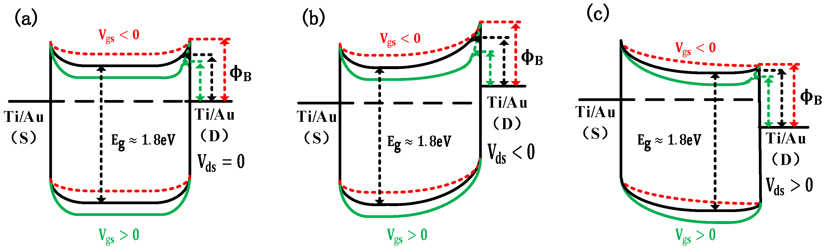
3. Results and Discussion
4. Conclusions
Supplementary Materials
Author Contributions
Funding
Conflicts of Interest
References
- Radisavljevic, B.; Radenovic, A.; Brivio, J.; Giacometti, V.; Kis, A. Single-layer MoS2 transistors. Nat. Nanotechnol. 2011, 6, 147. [Google Scholar] [CrossRef] [PubMed]
- Liu, W.; Kang, J.; Sarkar, D.; Khatami, Y.; Jena, D.; Banerjee, K. Role of metal contacts in designing high-performance monolayer n-type WSe2 field effect transistors. Nano Lett. 2013, 13, 1983–1990. [Google Scholar] [CrossRef] [PubMed]
- Illarionov, Y.Y.; Smithe, K.K.; Waltl, M.; Knobloch, T.; Pop, E.; Grasser, T. Improved hysteresis and reliability of MoS2 transistors with high-quality CVD growth and Al2O3 encapsulation. IEEE Electron. Device Lett. 2017, 38, 1763–1766. [Google Scholar] [CrossRef]
- Di Bartolomeo, A.; Pelella, A.; Liu, X.; Miao, F.; Passacantando, M.; Giubileo, F.; Grillo, A.; Iemmo, L.; Urban, F.; Liang, S.J. Pressure-Tunable Ambipolar Conduction and Hysteresis in Thin Palladium Diselenide Field Effect Transistors. arXiv 2019, arXiv:1902.00560. [Google Scholar] [CrossRef]
- Lin, J.; Li, H.; Zhang, H.; Chen, W. Plasmonic enhancement of photocurrent in MoS2 field-effect-transistor. Applied. Phys. Lett. 2013, 102, 203109. [Google Scholar]
- Kim, C.; Moon, I.; Lee, D.; Choi, M.S.; Ahmed, F.; Nam, S.; Cho, Y.; Shin, H.J.; Park, S.; Yoo, W.J. Fermi level pinning at electrical metal contacts of monolayer molybdenum dichalcogenides. ACS Nano 2017, 11, 1588–1596. [Google Scholar] [CrossRef] [PubMed]
- Islam, A.; Lee, J.; Feng, P.X.L. All-dry transferred single-and few-layer MoS2 field effect transistor with enhanced performance by thermal annealing. J. Appl. Phys. 2018, 123, 025701. [Google Scholar] [CrossRef]
- Wang, J.; Yao, Q.; Huang, C.W.; Zou, X.; Liao, L.; Chen, S.; Fan, Z.; Zhang, K.; Wu, W.; Xiao, X.; et al. High mobility MoS2 transistor with low schottky barrier contact by using atomic thick h-BN as a tunneling layer. Adv. Mater. 2016, 28, 8302–8308. [Google Scholar] [CrossRef]
- Kim, G.S.; Kim, S.H.; Park, J.; Han, K.H.; Kim, J.; Yu, H.Y. Schottky Barrier Height Engineering for Electrical Contacts of Multilayered MoS2 Transistors with Reduction of Metal-Induced Gap States. ACS Nano 2018, 12, 6292–6300. [Google Scholar] [CrossRef]
- Kaushik, N.; Karmakar, D.; Nipane, A.; Karande, S.; Lodha, S. Interfacial n-doping using an ultrathin TiO2 layer for contact resistance reduction in MoS2. ACS Appl. Mater. Interfaces 2015, 8, 256–263. [Google Scholar] [CrossRef]
- Chee, S.S.; Seo, D.; Kim, H.; Jang, H.; Lee, S.; Moon, S.P.; Lee, K.H.; Kim, S.W.; Choi, H.; Ham, M.H. Lowering the Schottky Barrier Height by Graphene/Ag Electrodes for High-Mobility MoS2 Field-Effect Transistors. Adv. Mater. 2019, 31, 1804422. [Google Scholar] [CrossRef] [PubMed]
- Ganapathi, K.L.; Bhattacharjee, S.; Mohan, S.; Bhat, N. High-performance HfO2 back gated multilayer MoS2 transistors. IEEE Electron. Device Lett. 2016, 37, 797–800. [Google Scholar]
- Das, S.; Chen, H.Y.; Penumatcha, A.V.; Appenzeller, J. High performance multilayer MoS2 transistors with scandium contacts. Nano Lett. 2012, 13, 100–105. [Google Scholar] [CrossRef] [PubMed]
- Sze, S.M.; Ng, K.K. Physics of Semiconductor Devices, 3rd ed.; Wiley-Interscience: Hoboken, NJ, USA, 2007. [Google Scholar]
- Miao, J.; Hu, W.; Jing, Y.; Luo, W.; Liao, L.; Pan, A.; Wu, S.; Cheng, J.; Chen, X.; Lu, W. Surface plasmon-enhanced photodetection in few layer MoS2 phototransistors with Au nanostructure arrays. Small 2015, 11, 2392–2398. [Google Scholar] [CrossRef] [PubMed]
- Zheng, J.; Yan, X.; Lu, Z.; Qiu, H.; Xu, G.; Zhou, X.; Wang, P.; Pan, X.; Liu, K.; Jiao, L. High-Mobility Multilayered MoS2 Flakes with Low Contact Resistance Grown by Chemical Vapor Deposition. Adv. Mater. 2017, 29, 1604540. [Google Scholar] [CrossRef]
- Yang, P.; Yang, A.G.; Chen, L. Influence of seeding promoters on the properties of CVD grown monolayer molybdenum disulfide. Nano Res. 2019, 12, 823–827. [Google Scholar] [CrossRef]
- Chen, J.; Zhao, X.; Tan, S.J.; Xu, H.; Wu, B.; Liu, B.; Fu, D.; Fu, W.; Geng, D.; Liu, Y.; et al. Chemical vapor deposition of large-size monolayer MoSe2 crystals on molten glass. J. Am. Chem. Soc. 2017, 139, 1073–1076. [Google Scholar] [CrossRef]
- Liu, Y.; Guo, J.; Zhu, E.; Liao, L.; Lee, S.J.; Ding, M.; Shakir, I.; Gambin, V.; Huang, Y.; Duan, X. Approaching the Schottky–Mott limit in van der Waals metal–semiconductor junctions. Nature 2018, 557, 696. [Google Scholar] [CrossRef]
- Chanana, A.; Mahapatra, S. Prospects of zero Schottky barrier height in a graphene-inserted MoS2-metal interface. J. Appl. Phys. 2016, 119, 014303. [Google Scholar] [CrossRef]
- Liu, T.; Liu, S.; Tu, K.H.; Schmidt, H.; Chu, L.; Xiang, D.; Martin, J.; Eda, G.; Ross, C.A.; Garaj, S. Crested two-dimensional transistors. Nat. Nanotechnol. 2019, 14, 223. [Google Scholar] [CrossRef]
- Sze, S.M.; Coleman, D.J., Jr.; Loya, A. Current transport in metal-semiconductor-metal (MSM) structures. Solid-State Electron. 1971, 14, 1209–1218. [Google Scholar] [CrossRef]
- Di Bartolomeo, A.; Giubileo, F.; Luongo, G.; Iemmo, L.; Martucciello, N.; Niu, G.; Fraschke, M.; Skibitzki, O.; Schroeder, T.; Lupina, G. Tunable Schottky barrier and high responsivity in graphene/Si-nanotip optoelectronic device. 2D Mater. 2016, 4, 015024. [Google Scholar] [CrossRef]
- Sarkar, D.; Xie, X.; Liu, W.; Cao, W.; Kang, J.; Gong, Y.; Kraemer, S.; Ajayan, P.M.; Banerjee, K. A subthermionic tunnel field-effect transistor with an atomically thin channel. Nature 2015, 526, 91. [Google Scholar] [CrossRef] [PubMed]
- Shin, G.H.; Koo, B.; Park, H.; Woo, Y.; Lee, J.E.; Choi, S.Y. Vertical-tunnel field-effect transistor based on a silicon–MoS2 Three-dimensional–two-dimensional heterostructure. ACS Appl. Mater. Interfaces 2018, 10, 40212–40218. [Google Scholar] [CrossRef] [PubMed]
- Wang, X.F.; Tian, H.; Liu, Y.; Shen, S.; Yan, Z.; Deng, N.; Yang, Y.; Ren, T.L. Two-Mode MoS2 Filament Transistor with Extremely Low Subthreshold Swing and Record High On/Off Ratio. ACS Nano 2019, 13, 2205–2212. [Google Scholar] [CrossRef] [PubMed]
- Moriya, R.; Yamaguchi, T.; Inoue, Y.; Morikawa, S.; Sata, Y.; Masubuchi, S.; Machida, T. Large current modulation in exfoliated-graphene/MoS2/metal vertical heterostructures. Appl. Phys. Lett. 2014, 105, 083119. [Google Scholar] [CrossRef]


© 2019 by the authors. Licensee MDPI, Basel, Switzerland. This article is an open access article distributed under the terms and conditions of the Creative Commons Attribution (CC BY) license (http://creativecommons.org/licenses/by/4.0/).
Share and Cite
Yang, K.; Liu, H.; Wang, S.; Li, W.; Han, T. A Horizontal-Gate Monolayer MoS2 Transistor Based on Image Force Barrier Reduction. Nanomaterials 2019, 9, 1245. https://doi.org/10.3390/nano9091245
Yang K, Liu H, Wang S, Li W, Han T. A Horizontal-Gate Monolayer MoS2 Transistor Based on Image Force Barrier Reduction. Nanomaterials. 2019; 9(9):1245. https://doi.org/10.3390/nano9091245
Chicago/Turabian StyleYang, Kun, Hongxia Liu, Shulong Wang, Wei Li, and Tao Han. 2019. "A Horizontal-Gate Monolayer MoS2 Transistor Based on Image Force Barrier Reduction" Nanomaterials 9, no. 9: 1245. https://doi.org/10.3390/nano9091245
APA StyleYang, K., Liu, H., Wang, S., Li, W., & Han, T. (2019). A Horizontal-Gate Monolayer MoS2 Transistor Based on Image Force Barrier Reduction. Nanomaterials, 9(9), 1245. https://doi.org/10.3390/nano9091245