Article

Production of SnS2 Nanostructure as Improved Light-Assisted Electrochemical Water Splitting

1
Collaborative Innovation Center of Advanced Microstructures, Nanjing University, Nanjing 210093, China
2
School of Electronic Science and Engineering, Nanjing University, Nanjing 210093, China
3
School of Geography and Biological Information, Nanjing University of Posts and Telecommunications, Nanjing 210023, China
*
Authors to whom correspondence should be addressed.
Nanomaterials 2019, 9(9), 1244; https://doi.org/10.3390/nano9091244
Submission received: 7 August 2019 / Revised: 26 August 2019 / Accepted: 28 August 2019 / Published: 1 September 2019

Abstract

:
Tin disulfide (SnS2) has gained a lot of interest in the field of converting solar energy into chemical fuels in light-assisted electrochemical water splitting due to its visible-light band gap and high electronic mobility. However, further decreasing the recombination rate of electron-hole pairs and increasing the density of active states at the valence band edge of the photoelectrodes were a critical problem. Here, we were successful in fabricating the super-thin SnS2 nanostructure by a hydrothermal and solution etching method. The super-thin SnS2 nanostructure as a photo-electrocatalytic material exhibited low overpotential of 0.25 V at the current density of −10 mA·cm−2 and the potential remained basically unchanged after 1000 cycles in an H2SO4 electrolyte solution, which was better than that of the SnS2 nanosheet and SnS/SnS2 heterojunction nanosheet. These results show the potential application of super-thin SnS2 nanostructure in electrochemical/photo-electrocatalytic field.

1. Introduction

In recent years, there has been more and more research on the application of two-dimensional (2D) layered materials as field-effect-transistors (FETs) [1,2], photodetectors [3,4], photocatalysis [5], lithium-ion battery, etc. [6,7,8,9], which were dependent on the excellent electronic mobility and optical properties [10,11]. Besides, 2D layered materials have also been considered as a photocatalysis to water splitting in the next generation since its 2D conductive channel is beneficial to fast carrier transport and greatly reduce the recombination rate in the photoelectrode, and the larger surface area is conducive to rapid charge transfer and enhance electrochemical reaction at the interface, which could improve the reaction efficiency [12,13,14]. As an original member of semiconductor metal sulfides family, the hexagonal SnS2 is nontoxic, inexpensive, chemically stable in acidic and neutral solutions, and visible-light band gap of 2.2–2.4 eV [14,15,16]. In the last few years, it has been proved to be a promising photocatalyst in the application of dye degradation processes.
Recently, the SnS2 has been considered as a photo-electric-catalyst for water splitting. Sun et al. [12] first synthesized freestanding SnS2 single layers with three atom thickness by liquid exfoliation. The SnS2 single layers displayed excellent structural stability and increased density of states at the valence band edge, which achieved efficient visible light water splitting. Further, a series of regular hexagon-shaped SnS2 nanoplates were fabricated via a facile hydrothermal process by Fu et al. [16]. The SnS2 nanoplate-like products can efficiently delay photogenerated charge recombination, which showed good photocatalytic activity for H2 production. Moreover, Meng and co-workers [14] reported improved photoelectrochemical water splitting based on doped SnS2 nanosheet arrays with amorphization, vacancy, and gradient energy band through a hydrothermal method. Taking the above reports, SnS2 plays a key role in enhancing the visible light photocatalytic of water splitting. In this work, we reported the facile synthesis of super-thin SnS2 nanostructure via hydrothermal and solution etching method and applied it to light-assisted electrochemical water splitting. It is expected to exhibit better performance in light-assisted electrochemical water splitting.

2. Experimental Details

2.1. Preparation of SnS2 Nanostructure

All chemical reagents were of analytical grade and were used without further purification. SnCl4·5H2O, thiourea, and sulfur ammonia were purchased from Aladdin Industrial Corporation.
In the typical experiment, SnS2 nanostructure was synthesized by the solvothermal and etching solution methods. Briefly, 0.1753 g of SnCl4·5H2O and 0.0952 g of thiourea were dissolved in 30 mL of ethylene glycol by ultrasound to give a transparent solution. The mixture was then transferred into a Teflon-lined autoclave (50 mL) in an oven at 180 °C for 24 h. After cooling to room temperature, the precipitate was collected from the solution through centrifugal filtration, followed by washing several times using distilled water to remove the organic residues, and dried at 60 °C for 6 h. Next, the SnS/SnS2 heterojunctions were obtained by heat treatment at 500 °C for 30 min under Ar atmosphere. Finally, in order to obtain the SnS2 nanostructure by the etching solution method with sulfur ammonia for 20 min (10 and 30 min), the sample was washed several times using distilled water, and dried at 60 °C.

2.2. Materials Characterizations

Sample morphology was studied by a field-emission scanning electron microscope (FESEM; FE-SEM; JSM-7000F, JEOL Ltd., Tokyo, Japan). Transmission electron microscopy (TEM) and high-resolution transmission electron microscopy (HRTEM) images were obtained using a JEOL model JEM2100 instrument at an accelerating voltage of 200 kV (JEOL Ltd., Tokyo, Japan). The crystal phase properties of the samples were analyzed with a Bruker D8 Advance X-ray diffractometer (XRD) using Ni-filtered Cu Kα radiation at 40 kV, 40 mA and 2θ range from 10° to 60° with a scan rate of 0.1° per second (Bruker Daltonics Inc., Karlsruhe, Germany). Raman spectra were obtained using a Raman spectrometer (JY T64000) excited by the 488 nm line of an Ar+ laser under 22 mW (HORIBA, Ltd., Kyoto, Japan). Atomic force microscopy (AFM) images were taken by Cypher S microscopy (Oxford Instruments Asylum Research, California, USA). X-ray photoelectron spectroscopy (XPS) analysis (PHI5000 Versaprobe) was used to determine the chemical composition of the products (Ulvac-Phi Inc., Kanagawa, Japan).

2.3. Light-Assisted Electrochemical Water Splitting Measurements

Light-assisted electrocatalytic activity was measured at 25 °C in a three-electrode cell connected to a CHI-760E workstation (CH Instruments, Chenhua Co., Shanghai, China). SnS2 nanostructure (10 mg) (SnS2 and SnS/SnS2 heterojunction), acetylene carbon (1 mg), and 5 % polyvinylidene fluoride dimethylformamide solution (20 mg) were all mixed together. The obtained slurry was then coated onto carbon paper and then dried to form a thin-film electrode which was used as the working electrode. Meanwhile, Ag/AgCl (KCl filled) and a platinum wire both served as reference and counter electrodes, respectively. A 0.5 mol·L−1 H2SO4 solution was used as an electrolyte. The cell geometry is dual channel electrolytic cell. A 300 W Xe lamp served as a light source in the light-assisted electrochemical water splitting measurements. The lamp provided directional light with uniform intensity distribution and was filtered to simulate the solar spectrum before illuminating the sample. Polarization curves at a scan rate of 5 mV·s−1 were conducted in the above H2SO4 solution between 0 and −1 V. The light-assisted electrochemical water splitting performance of SnS2 nanosheet and SnS/SnS2 heterojunction were also measured by the same method.

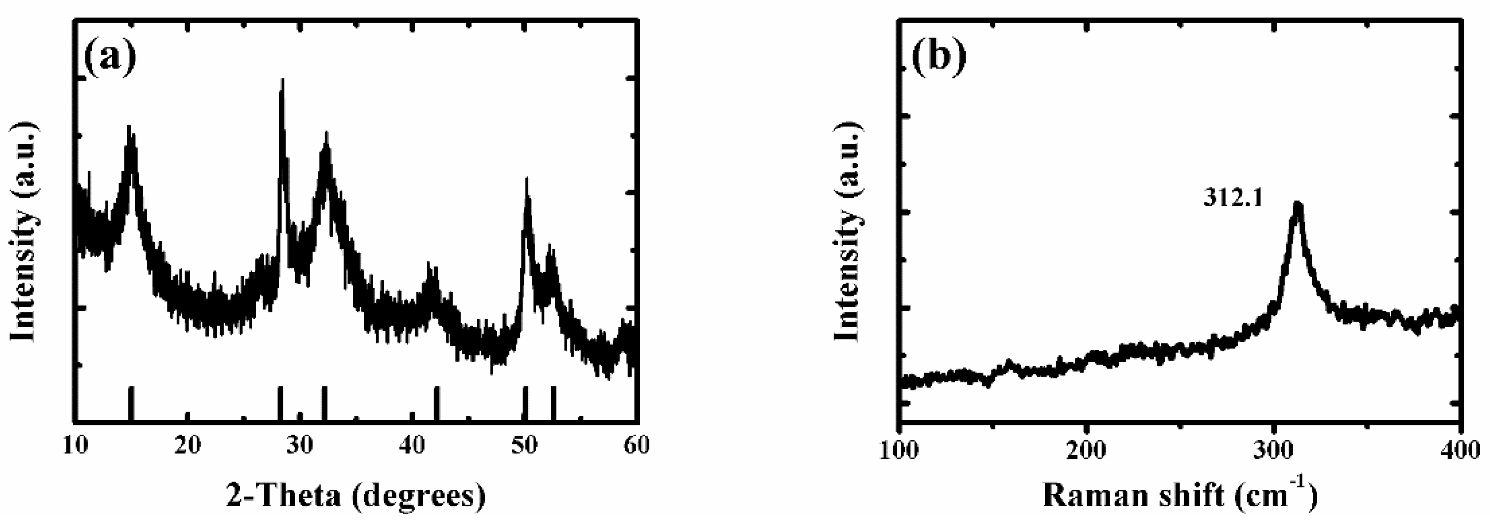
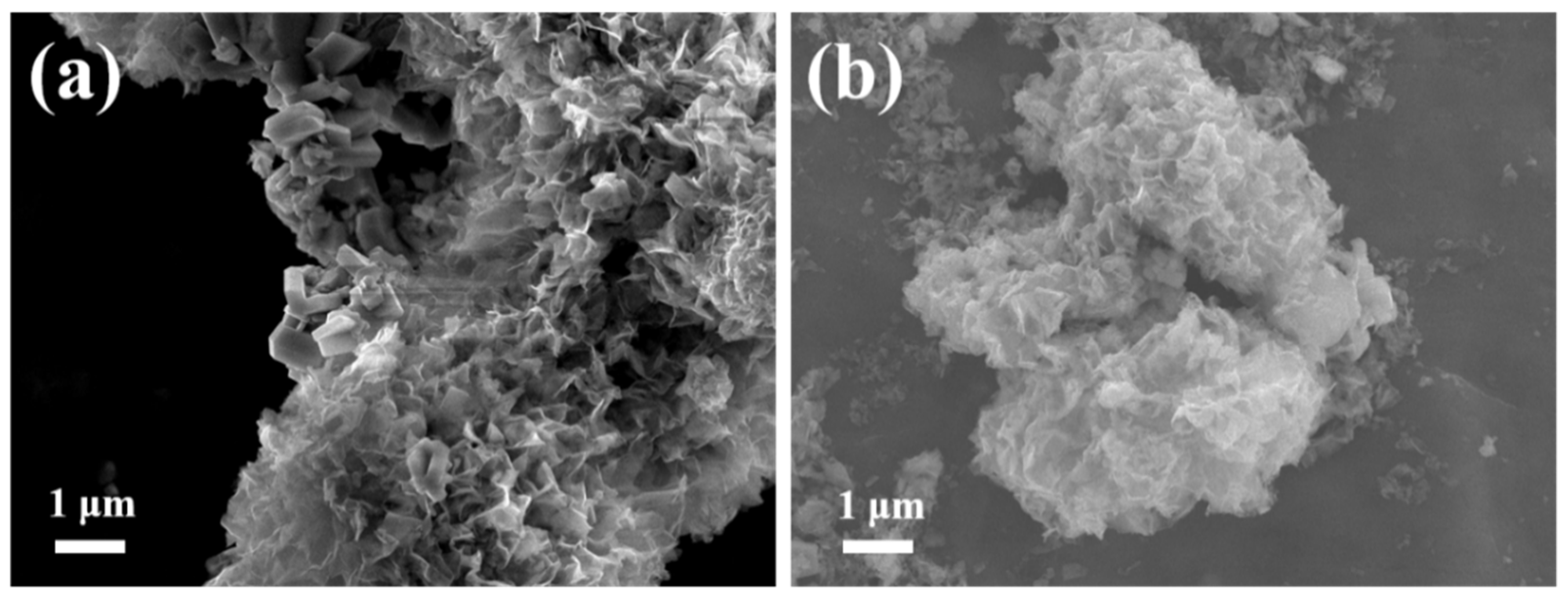
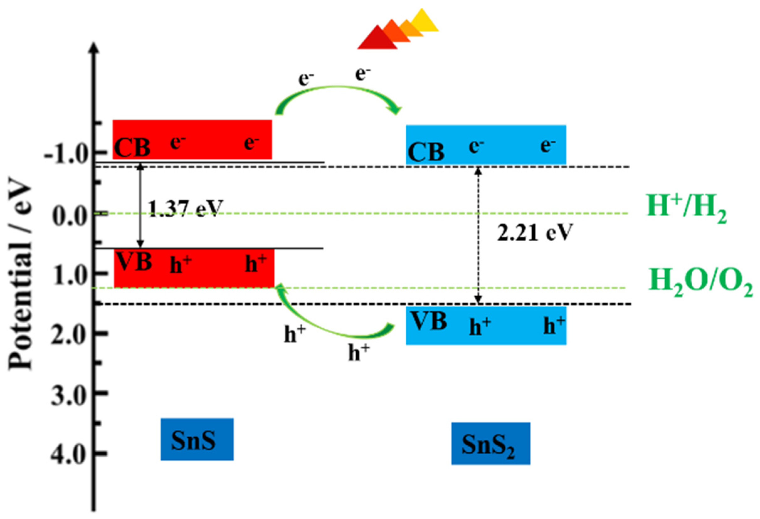
3. Results and Discussion

SnS/SnS2 heterojunction could be synthesized through the hydrothermal and low-temperature annealing method. Then, the super-thin SnS2 nanostructure was obtained by the reaction between SnS/SnS2 heterojunction with ammonium persulfide. The conversion reactions:
SnS + (NH4)2S2→(NH4)2 SnS3
SnS2 + (NH4)2S→(NH4)2SnS3
(NH4)2S2→(NH4)2S + S
As the ammonium persulfide solution reacted only with tin sulfide (from reaction (1)), the tin disulfide was retained. Because ammonium persulfide has poor stability at room temperature, some of the ammonium persulfides may be converted to ammonium sulfide (from reaction (3)) during the reaction. The tin sulfide will continue to react with ammonium sulfide (from reaction (2)). Therefore, samples with different morphologies can be obtained with different reaction times. From scanning electron microscopy (SEM), it was found that the mechanism was proved correct (see below). Therefore, the super-thin SnS2 nanostructure showed a thinner thickness and a smaller size and exhibited excellent light-assisted electrochemical water splitting performance. As shown in Figure A1a and Figure 1a, the X-ray diffraction (XRD) patterns of SnS2 nanosheet, SnS/SnS2 heterojunction nanosheet and super-thin SnS2 nanostructure samples were well crystallized. Moreover, all diffraction peaks of samples were very sharp, which indicated a high crystallinity. It was observed that diffraction peaks of the super-thin SnS2 nanostructure at 15.2, 28.2, 32.1, 41.9, 50.0, and 52.5° can be assigned to the (001), (100), (101), (102), (110), and (111) planes, respectively. Compared with SnS2 nanosheet and SnS/SnS2 heterojunction nanosheet (Figure A1a), we found that all the diffraction peaks of the super-thin SnS2 nanostructure were indexed to the hexagonal SnS2 (JCPDS No. 23-0677) [17,18,19]. In addition, it was found that there are no impurity peaks in the figures, indicating that the SnS2 material was obtained after solution etching. Furthermore, in order to demonstrate the sample was the super-thin SnS2 nanostructure after solution etching, the Raman analyzer was used to study the chemical structure (Figure A1b and Figure 1b). From the spectra in Figure A1b, the peaks of Raman spectra at 182, 220, and 312 cm−1 were SnS and SnS2, respectively. And Figure 1b shows the Raman spectra of the super-thin SnS2 nanostructure. The peak at 312.1 cm−1 was matched well with hexagonal SnS2 [20,21,22].
Moreover, Figure 2, Figure A2 and Figure A3 show the field-emission scanning electron microscopy (HESEM) and transmission electron microscopy (TEM) images of the super-thin SnS2 nanostructure. The typical FESEM image of the super-thin SnS2 nanostructure displayed a typical super-thin nanosheet morphology. Moreover, in contrast with the FESEM of the SnS2 nanosheet and SnS/SnS2 heterojunction nanosheet in Figure A2, the super-thin SnS2 nanostructure showed the thinner nanostructure. This super-thin nanostructure could improve fast carrier transport and greatly reduce the recombination rate [12,23,24]. Figure 2b reveals the FESEM and energy-dispersive spectrometry (EDS) of the super-thin SnS2 nanostructure, the elemental mapping images confirm that the elements Sn and S were uniformly distributed among the sample [25,26]. Moreover, Figure A3 also shows the elements were uniformly distributed in the samples by the different time of solution etching. The uniform morphologies of the super-thin SnS2 nanostructure were also investigated by the TEM in Figure 2c,d. The super-thin SnS2 nanostructure with a lateral size of about 1 μm was observed. Additionally, the high-resolution transmission electron microscopy (HRTEM) image taken from the selected area in Figure 1c is shown in Figure 1d, which exhibited a crystal lattice spacing of 0.28 nm and belonged to the crystal facet (101) of hexagonal SnS2 [19,27,28]. Figure 2e,f shows the atomic force microscope (AFM) images of the SnS2 nanosheet and super-thin SnS2 nanostructure, which can further characterize the size and morphology. Figure 2f shows the super-thin SnS2 nanostructure with a thickness of 1.7 nm and lateral dimension of ~ 250 nm. Due to the above results, the super-thin SnS2 nanostructure showed a thinner nanostructure and a larger specific surface area than the SnS2 nanosheet. Therefore, the super-thin SnS2 nanostructure would exhibit excellent light-assisted electrochemical activity performance.
To further confirm the surface-chemical states of the super-thin SnS2 nanostructure, the X-ray photoelectron spectroscopy (XPS) spectra were characterized in Figure 3. Figure 3a shows the wide scan spectrum of the super-thin SnS2 nanostructure, the Sn, S, C, and O elements were detected. It was indicated that the sample contained those elements and no other impurities could be found. The peaks at 495.2 and 486.6 eV were observed in Figure 3b, which was recognized as the 3d3/2 and 3d5/2 states of Sn4+ for the hexagonal SnS2 [8,14]. Moreover, the high-resolution XPS spectra for S 2p can be fitted with two peaks of 164.3 and 163.0 eV, corresponding to 2p1/2 and 2p3/2 states of S2-, respectively [29,30,31]. From the XRD, Raman, FESEM, TEM, and XPS data representation, the super-thin SnS2 nanostructure was successfully fabricated through the hydrothermal and solution etching method.
To evaluate the light-assisted electrochemical water splitting performance, the super-thin SnS2 nanostructure, SnS2 nanosheet, and SnS/SnS2 heterojunction sheet were measured by the typical three-electrode cell connected with a CHI 670E configuration in 0.5 M H2SO4 solution under a 300 W Xe lamp at the room temperature [14,16,32,33,34,35]. Figure 4a shows the linear sweep voltammetry (LSV) curves of the samples. The SnS2 nanosheet displayed poorer photocatalytic activity than the SnS/SnS2 heterojunction sheet. SnS/SnS2 heterojunction sheet showed improved light-assisted electrochemical water splitting performance, which depended on its specific energy band structure (Figure A4 shows that the photo-generated electrons on the CB of SnS can easily flow to the CB of SnS2 through the interface. In the same way, the holes on the VB of SnS2 are more positive than those of SnS and can be transferred to the VB of SnS and the VB edge level of SnS2. It can be efficient electron-hole pair separation and enhance photocatalytic activity). However, the super-thin SnS2 nanostructure displayed an overpotential of 0.25 V at the current density of −10 mA cm−2, which exhibited better overpotential than the SnS2 nanosheet and SnS/SnS2 heterojunction sheet and proved its superior hydrogen evolution reaction (HER) activity by the higher electrochemically active surface areas (Figure 4c and Figure A7). Meanwhile, to check the durability of the super-thin SnS2 nanostructure, the basically unchanged LSV curves can be observed from comparing before and after 1000 cycles. Additionally, as the as-prepared SnS2 nanostructures were further compared with different times of solution etching, the samples were also analyzed by the LSV curves under the same conditions in Figure A5. The sample with 20 min solution etching (super-thin SnS2 nanostructure) displayed the best HER performance of all samples (solution etching 10 and 30 min). Therefore, the electrochemically active surface areas (ECSA) of the super-thin SnS2 nanostructure, SnS2 nanosheet and SnS/SnS2 heterojunction sheet were measured by the double-layer capacitances (Cdl). The Cdl was estimated through the investigated cycling voltammetry (CV) curves at different scan rates under non-faradaic region (Figure A6). As shown in Figure 4c, the super-thin SnS2 nanostructure exhibited larger Cdl value than that of SnS2 nanosheet and SnS/SnS2 heterojunction sheet. Interestingly, the super-thin SnS2 nanostructure exhibited larger ECSA than SnS2 nanosheet, which was regarded as higher catalytic activity. Moreover, better intrinsic catalytic activity for super-thin SnS2 nanostructure was further proved by its ECSA-corrected current densities in comparison with SnS2 nanosheet and SnS/SnS2 heterojunction in Figure A7 (detailed discussion in Appendix A). Due to the above results, the super-thin SnS2 nanostructure has a higher active surface area and more active sites, which can enhance HER property.

4. Conclusions

In summary, the super-thin SnS2 nanostructure has been successfully synthesized through a hydrothermal and solution etching route. The super-thin SnS2 nanostructure offered excellent light-assisted electrochemical water splitting performance due to effectively capturing visible light, enhancing carrier density, rapid charge transfer and fast chemical reaction. Given these unique benefits, we believe that super-thin SnS2 nanostructure built on the other trend can provide a new potential application for electrochemical/photo-electrocatalytic devices.

Author Contributions

The experiments and characterizations were carried out by H.S., with the assistance of H.W., Y.G., K.W. and X.S. under the guidance of S.Y. and Y.S., H.S. and S.Y. wrote the manuscript and prepared all figures. Y.S. and S.Y. supervised and coordinated all the work.

Funding

This research was funded by National Basic Research Program of China (973 Program: 2018YFA0209101), the National Science Foundations of China (No. 61205057, No. 11574136).

Acknowledgments

This work is supported by the National Basic Research Program of China (973 Program: 2018YFA0209101), the National Science Foundations of China (No. 61205057, No. 11574136).

Conflicts of Interest

The authors declare no conflict of interest.

Appendix A

Figure A1. (a) XRD pattern of the SnS2 nanosheets and SnS/SnS2 heterojunction. (b) Raman spectra of the SnS2 nanosheets and SnS/SnS2 heterojunction.
Nanomaterials 09 01244 g0a1
Figure A2. (a) The FESEM of the SnS2 nanosheets, (b) the FESEM of the SnS/SnS2 heterojunction.
Nanomaterials 09 01244 g0a2
Figure A3. (a) The FESEM image of the SnS2 nanosheet with solution etching 10 min. (b) The FESEM image and EDS of the SnS2 nanosheet with solution etching 10 min. (c) The FESEM image of the SnS2 nanosheet with solution etching 30 min. (d) The FESEM image and EDS of the SnS2 nanosheet with solution etching 30 min.
Nanomaterials 09 01244 g0a3
Figure A4. Schematic diagram for energy band matching and electron–hole separations.
Nanomaterials 09 01244 g0a4
The SnS/SnS2 heterojunction nanosheet acts as a photocathode, the catalytic mechanisms may be responsible for the following reasons: As shown in Figure A5, when SnS2 is in contact with SnS to form p-n heterostructure, these photo-generated electrons on the CB of SnS can easily flow to the CB of SnS2 through the interface. It is considered that the CB position of SnS is more negative than the CB position of SnS2. In the same way, the holes on the VB of SnS2 tend to transfer to the VB of SnS and the VB edge level of SnS2 is more positive than that of SnS, which can cause efficient electron-hole pair separation and thus lead to enhanced photocatalytic activity.
Figure A5. LSV curves of the SnS2 nanosheet by solution etching 10, 20, and 30 min with HER in 0.5 M H2SO4 solution.
Nanomaterials 09 01244 g0a5
Figure A6. Cyclic voltammograms of (a) SnS2 nanosheets, (b) SnS/SnS2 heterojunction and (c) SnS2 nanostructure were measured in the non-faradaic capacitance current range at scan rates of 5, 10, 20, 30, 40, 50, 60 70, 80, 90, and 100 mV s−1.
Nanomaterials 09 01244 g0a6
Figure A7. ECSA-corrected current densities versus applied potentials.
Nanomaterials 09 01244 g0a7
To measure electrochemical double-layer capacitance (Cdl), the potential was swept nine times at each scan rate (5,10, 20, 30, 40, 50, 60, 70, 80, 90, and 100 mV/s) in the scan range from −0.20 to 0 V vs. RHE. Capacitive currents were measured in a potential range where no faradic processes were observed. The measured capacitive currents difference (∆J) at −0.05 V vs. RHE was plotted against scan rate and specific capacitance was determined from the slope of the linear fitting. The Cdl values for SnS2 nanosheet and SnS/SnS2 heterojunction sheet and super-thin SnS2 nanostructure are calculated to be 0.178, 0.206, and 0.226 mF·cm−2, respectively. The specific capacitance is converted into an electrochemical surface area (ECSA) using the specific capacitance value for a flat standard with 1 cm2 of real surface area. We use the specific capacitance (20–60 μF cm−2) of 40 μF cm−2 here to calculate the ECSA (Nature Communications, 2018, 9, 2452. and Nature Communications, 2019, 10, 399.) according to Equation (A1):
ECSA = C d l 40   μ F / c m 2 c m E C S A 2
Calculated electrochemical active surface area:
SnS2 sheet:
A E C S A S n S 2 = 0.178 m F   c m 2 40   μ F   c m 2   p e r   c m E C S A 2   = 4.45   c m E C S A 2
SnS/SnS2 heterojunction sheet:
A E C S A S n S / S n S 2 = 0.206 m F   c m 2 40   μ F   c m 2   p e r   c m E C S A 2 = 5.15   c m E C S A 2
Super-thin SnS2 nanostructure:
A E C S A S S n S 2 = 0.226 m F   c m 2 40   μ F   c m 2   p e r   c m E C S A 2 = 5.65   c m E C S A 2

References

  1. Wang, Y.; Kim, J.C.; Wu, R.J.; Martinez, J.; Song, X.; Yang, J.; Zhao, F.; Mkhoyan, A.; Jeong, H.Y.; Chhowalla, M. Van der Waals contacts between three-dimensional metals and two-dimensional semiconductors. Nature 2019, 568, 70–74. [Google Scholar] [CrossRef] [PubMed]
  2. Illarionov, Y.Y.; Banshchikov, A.G.; Polyushkin, D.K.; Wachter, S.; Knobloch, T.; Thesberg, M.; Mennel, L.; Paur, M.; Stöger-Pollach, M.; Steiger-Thirsfeld, A.; et al. Ultrathin calcium fluoride insulators for two-dimensional field-effect transistors. Nat. Electron. 2019, 2, 230–235. [Google Scholar] [CrossRef]
  3. Yin, J.; Tan, Z.; Hong, H.; Wu, J.; Yuan, H.; Liu, Y.; Chen, C.; Tan, C.; Yao, F.; Li, T. Ultrafast and highly sensitive infrared photodetectors based on two-dimensional oxyselenide crystals. Nat. Commun. 2018, 9, 3311. [Google Scholar] [CrossRef] [PubMed]
  4. Konstantatos, G. Current status and technological prospect of photodetectors based on two-dimensional materials. Nat. Commun. 2018, 9, 5266. [Google Scholar] [CrossRef] [PubMed]
  5. Liu, G.; Zhen, C.; Kang, Y.; Wang, L.; Cheng, H.M. Unique physicochemical properties of two-dimensional light absorbers facilitating photocatalysis. Chem. Soc. Rev. 2018, 47, 6410–6444. [Google Scholar] [CrossRef]
  6. Chen, C.; Xie, X.; Anasori, B.; Sarycheva, A.; Makaryan, T.; Zhao, M.; Urbankowski, P.; Miao, L.; Jiang, J.; Gogotsi, Y. MoS2-on-MXene heterostructures as highly reversible anode materials for lithium-ion batteries. Angew. Chem. Int. Ed. 2018, 57, 1846–1850. [Google Scholar] [CrossRef] [PubMed]
  7. Yan, S.; Wang, B.; Wang, Z.; Hu, D.; Xu, X.; Wang, J.; Shi, Y. Supercritical carbon dioxide-assisted rapid synthesis of few-layer black phosphorus for hydrogen peroxide sensing. Biosens. Bioelectron. 2016, 80, 34–38. [Google Scholar] [CrossRef] [Green Version]
  8. Khan, Z.; Parveen, N.; Ansari, S.A.; Senthilkumar, S.T.; Park, S.; Kim, Y.; Cho, M.H.; Ko, H. Three-dimensional SnS2 nanopetals for hybrid sodium-air batteries. Electrochim. Acta 2017, 257, 328–334. [Google Scholar] [CrossRef]
  9. Khan, Z.; Park, S.; Hwang, S.M.; Yang, J.; Lee, Y.; Song, H.K.; Kim, Y.; Ko, H. Hierarchical urchin-shaped α-MnO2 on graphene-coated carbon microfibers: A binder-free electrode for rechargeable aqueous Na–air battery. NPG Asia Mater. 2016, 8, e294. [Google Scholar] [CrossRef]
  10. Liu, Y.; Wang, J.; Kim, S.; Sun, H.; Yang, F.; Fang, Z.; Tamura, N.; Zhang, R.; Song, X.; Wen, J. Helical van der Waals crystals with discretized Eshelby twist. Nature 2019, 570, 358–362. [Google Scholar] [CrossRef] [Green Version]
  11. Lin, S.; Carvalho, A.; Yan, S.; Li, R.; Kim, S.; Rodin, A.; Carvalho, L.; Chan, E.M.; Wang, X.; Neto, A.H.C.; et al. Accessing valley degree of freedom in bulk Tin (II) sulfide at room temperature. Nat. Commun. 2018, 9, 1455. [Google Scholar] [CrossRef] [PubMed]
  12. Sun, Y.; Cheng, H.; Gao, S.; Sun, Z.; Liu, Q.; Liu, Q.; Lei, F.; Yao, T.; He, J.; Wei, S.; et al. Freestanding tin disulfide single-layers realizing efficient visible-light water splitting. Angew. Chem. Int. Ed. 2012, 51, 8727–8731. [Google Scholar] [CrossRef] [PubMed]
  13. Zhang, Y.C.; Du, Z.N.; Li, S.Y.; Zhang, M. Novel synthesis and high visible light photocatalytic activity of SnS2 nanoflakes from SnCl2·2H2O and S powders. Appl. Catal. B Environ. 2010, 95, 153–159. [Google Scholar] [CrossRef]
  14. Meng, L.; Wang, S.; Cao, F.; Tian, W.; Long, R.; Li, L. Doping-Induced Amorphization, Vacancy, and Gradient Energy Band in SnS2 Nanosheet Arrays for Improved Photoelectrochemical Water Splitting. Angew. Chem. Int. Ed. 2019, 58, 6761–6765. [Google Scholar] [CrossRef] [PubMed]
  15. Giri, B.; Masroor, M.; Yan, T.; Kushnir, K.; Carl, A.D.; Doiron, C.; Zhang, H.; Zhao, Y.; McClelland, A.; Tompsett, G.A. Balancing Light Absorption and Charge Transport in Vertical SnS2 Nanoflake Photoanodes with Stepped Layers and Large Intrinsic Mobility. Adv. Energy Mater. 2019, 9, 1901236. [Google Scholar] [CrossRef]
  16. Fu, W.; Wang, J.; Zhou, S.; Li, R.; Peng, T. Controllable fabrication of regular hexagon-shaped SnS2 nanoplates and their enhanced visible-light-driven H2 production activity. ACS Appl. Nano Mater. 2018, 1, 2923–2933. [Google Scholar] [CrossRef]
  17. Tu, F.; Xu, X.; Wang, P.; Si, L.; Zhou, X.; Bao, J. A few-layer SnS2/reduced graphene oxide sandwich hybrid for efficient sodium storage. J. Phys. Chem. C 2017, 121, 3261–3269. [Google Scholar] [CrossRef]
  18. Jiang, Y.; Wei, M.; Feng, J.; Ma, Y.; Xiong, S. Enhancing the cycling stability of Na-ion batteries by bonding SnS 2 ultrafine nanocrystals on amino-functionalized graphene hybrid nanosheets. Energy Environ. Sci. 2016, 9, 1430–1438. [Google Scholar] [CrossRef]
  19. Yan, S.; Li, K.; Lin, Z.; Song, H.; Jiang, T.; Wu, J.; Shi, Y. Fabrication of a reversible SnS2/RGO nanocomposite for high performance lithium storage. RSC Adv. 2016, 6, 32414–32421. [Google Scholar] [CrossRef]
  20. Gong, Y.; Yuan, H.; Wu, C.L.; Tang, P.; Yang, S.Z.; Yang, A.; Li, G.; Liu, B.; van de Groep, J.; Brongersma, M. Spatially controlled doping of two-dimensional SnS2 through intercalation for electronics. Nat. Nanotechnol. 2018, 13, 294–299. [Google Scholar] [CrossRef]
  21. Li, Q.; Wei, A.; Guo, Z.; Liu, J.; Zhao, Y.; Xiao, Z. Chemical vapor deposition of two-dimensional SnS 2 nanoflakes and flower-shaped SnS2. J. Mater. Sci. Mater. Electron. 2018, 29, 16057–16063. [Google Scholar] [CrossRef]
  22. Wang, S. Solvothermal synthesis of porous SnS2 nanotubes with higher adsorption and photocatalytic activity. Surf. Sci. 2019, 690, 121469. [Google Scholar] [CrossRef]
  23. Song, F.; Hu, X. Exfoliation of layered double hydroxides for enhanced oxygen evolution catalysis. Nat. Commun. 2014, 5, 4477. [Google Scholar] [CrossRef] [PubMed]
  24. Yu, J.; Xu, C.Y.; Ma, F.X.; Hu, S.P.; Zhang, Y.W.; Zhen, L. Monodisperse SnS2 nanosheets for high-performance photocatalytic hydrogen generation. ACS Appl. Mater. Interfaces 2014, 6, 22370–22377. [Google Scholar] [CrossRef] [PubMed]
  25. Liu, J.; Wang, J.; Zhang, B.; Ruan, Y.; Wan, H.; Ji, X.; Xu, K.; Zha, D.; Miao, L.; Jiang, J. Mutually beneficial Co3O4@ MoS2 heterostructures as a highly efficient bifunctional catalyst for electrochemical overall water splitting. J. Mater. Chem. A 2018, 6, 2067–2072. [Google Scholar] [CrossRef]
  26. Wang, J.; Luo, C.; Mao, J.; Zhu, Y.; Fan, X.; Gao, T.; Mignerey, A.C.; Wang, C. Solid-State Fabrication of SnS2/C Nanospheres for High-Performance Sodium Ion Battery Anode. ACS Appl. Mater. Interfaces 2015, 7, 11476–11481. [Google Scholar] [CrossRef] [PubMed]
  27. Jing, X.; Li, L.; Xie, J.; Yan, H.; Yuan, Y.; Chen, M.; Cheng, H.; Yue, Z.; Su, N.; Wang, X. Layer-by-layered SnS2/graphene hybrid nanosheets via ball-milling as promising anode materials for lithium ion batteries. Electrochim. Acta 2018, 269, 452–461. [Google Scholar]
  28. Wu, Y.; Nie, P.; Wu, L.; Dou, H.; Zhang, X. 2D MXene/SnS2 composites as high-performance anodes for sodium ion batteries. Chem. Eng. J. 2018, 334, 932–938. [Google Scholar] [CrossRef]
  29. Xie, Y.; Fan, M.; Shen, T.; Liu, Q.; Chen, Y. SnS2 nanoplates as stable anodes for sodium ion and lithium ion batteries. Mater. Technol.: Adv. Perform. Mater. 2016, 31, 646–652. [Google Scholar] [CrossRef]
  30. Li, K.; Yan, S.; Lin, Z.; Dai, X.; Qu, P. Preparation and lithium ion batteries properties of SnS2 nanoparticle/reduced graphene oxide nanosheet nanocomposites using supercritical carbon dioxide. Synth. Met. 2016, 217, 138–143. [Google Scholar] [CrossRef]
  31. Khan, Z.; Park, S.O.; Yang, J.; Park, S.; Shanker, R.; Song, H.K.; Kim, Y.; Kwak, S.K.; Ko, H. Binary N, S-doped carbon nanospheres from bio-inspired artificial melanosomes: A route to efficient air electrodes for seawater batteries. J. Mater. Chem. A 2018, 6, 24459–24467. [Google Scholar] [CrossRef]
  32. Jarne, C.; Paul, L.; Conesa, J.C.; Shleev, S.; De Lacey, A.L.; Pita, M. Underpotential Photoelectrooxidation of Water by SnS2-Laccase Co-catalysts on Nanostructured Electrodes with Only Visible-Light Irradiation. ChemElectroChem 2019, 6, 2755–2761. [Google Scholar] [CrossRef]
  33. Huang, P.C.; Shen, Y.M.; Brahma, S.; Shaikh, M.O.; Huang, J.L.; Wang, S.C. SnSx (x = 1, 2) nanocrystals as effective catalysts for photoelectrochemical water splitting. Catalysts 2017, 7, 252. [Google Scholar] [CrossRef]
  34. Liu, E.; Chen, J.; Ma, Y.; Feng, J.; Jia, J.; Fan, J.; Hu, X. Fabrication of 2D SnS2/g-C3N4 heterojunction with enhanced H2 evolution during photocatalytic water splitting. J. Colloid Interface Sci. 2018, 524, 313–324. [Google Scholar] [CrossRef] [PubMed]
  35. Zhou, G.; Shan, Y.; Wang, L.; Hu, Y.; Guo, J.; Hu, F.; Shen, J.; Gu, Y.; Cui, J.; Liu, L.; et al. Photoinduced semiconductor-metal transition in ultrathin troilite FeS nanosheets to trigger efficient hydrogen evolution. Nat. Commun. 2019, 10, 399. [Google Scholar] [CrossRef] [PubMed]
Figure 1. (a) The typical XRD pattern of the super-thin SnS2 nanostructure. (b) The typical Raman spectra of the super-thin SnS2 nanostructure.
Nanomaterials 09 01244 g001
Figure 2. (a) The typical field-emission scanning electron microscope (FESEM) image of the super-thin SnS2 nanostructure. (b) The typical FESEM image and the energy-dispersive spectrometry (EDS) of the super-thin SnS2 nanostructure. (c) The typical transmission electron microscopy (TEM) image of the super-thin SnS2 nanostructure. (d) The typical high-resolution transmission electron microscopy (HRTEM) image of the super-thin SnS2 nanostructure, (e,f) atomic force microscopy (AFM) image of SnS2 nanosheet and super-thin SnS2 nanostructure.
Nanomaterials 09 01244 g002
Figure 3. (a) Full XPS spectrum of the super-thin SnS2 nanostructure. (b) High-resolution XPS spectra of Sn 3d. (c) High resolution XPS spectra of S 2p.
Nanomaterials 09 01244 g003
Figure 4. (a) Linear sweep voltammetry (LSV) curves of the SnS2 nanosheets, SnS/SnS2 heterojunction and super-thin SnS2 nanostructure for hydrogen evolution reaction (HER) in 0.5 M H2SO4 solution. (b) LSV curves of the super-thin SnS2 nanostructure before and after 1000 cycles. (c) The capacitive currents at −0.05 V as a function of scan rate for SnS2 nanosheets, SnS/SnS2 heterojunction and super-thin SnS2 nanostructure.
Nanomaterials 09 01244 g004

