Blue Electroluminescent Al2O3/Tm2O3 Nanolaminate Films Fabricated by Atomic Layer Deposition on Silicon


School of Materials Science and Engineering, Tianjin Key Lab for Rare Earth Materials and Applications, Nankai University, Tianjin 300350, China
*
Authors to whom correspondence should be addressed.
Nanomaterials 2019, 9(3), 413; https://doi.org/10.3390/nano9030413
Submission received: 18 February 2019
/
Revised: 4 March 2019
/
Accepted: 8 March 2019
/
Published: 11 March 2019
(This article belongs to the Special Issue Synthesis and Modification of Nanostructured Thin Films)
Abstract
:Realization of a silicon-based light source is of significant importance for the future development of optoelectronics and telecommunications. Here, nanolaminate Al2O3/Tm2O3 films are fabricated on silicon utilizing atomic layer deposition, and intense blue electroluminescence (EL) from Tm3+ ions is achieved in the metal-oxide-semiconductor structured luminescent devices based on them. Precise control of the nanolaminates enables the study on the influence of the Tm dopant layers and the distance between every Tm2O3 layer on the EL performance. The 456 nm blue EL from Tm3+ ions shows a maximum power density of 0.15 mW/cm2. The EL intensities and decay lifetime decrease with excessive Tm dopant cycles due to the reduction of optically active Tm3+ ions. Cross-relaxation among adjacent Tm2O3 dopant layers reduces the blue EL intensity and the decay lifetime, which strongly depends on the Al2O3 sublayer thickness, with a critical value of ~3 nm. The EL is attributed to the impact excitation of the Tm3+ ions by hot electrons in Al2O3 matrix via Poole–Frenkel mechanism.
1. Introduction
Traditional electronic integrated circuits have been facing with a bottleneck in terms of power consumption, speed, and signal crosstalk as the communication frequency and bandwidth rise to a higher level. One possible solution is the optoelectronic integration which realizes photonic technologies on silicon chips [1,2,3,4]. However, applicable Si-based light sources have been unsolved for a long time. Rare earth (RE) ions are generally efficient luminescence centers in various matrixes. Nowadays diverse RE-doped insulating materials have been developed for the applications in solid state lasers and phosphors [5,6,7,8,9]. However, it has been widely known that the mismatch in the coordination structure and atomic size of silicon (tetrahedron) and RE ions (octahedron) limit the desired spectroscopic performance due to the clustering of RE ions in the Si host [10,11]. Aiming for the realization of compact Si-based optoelectronics, electroluminescence (EL) from RE3+ ions has been extensively reported in many compounds, such as SiNx, TiO2, and ZnO [12,13,14,15]. However, the efficiencies of the devices based on the aforementioned materials are far from practical utilization. One of the limitations is the large leakage current. RE-implanted SiO2 MOS-structured light-emitting devices (MOSLEDs) have attracted much attention due to their notable EL efficiency and silicon compatibility [16,17]. In comparison, similar devices based on Al2O3 nanofilms present much lower working voltage, and comparable efficiency in our previous study, while their EL performance needs more exploration [18,19]. Blue emission, which has the highest photon energy (2.6–2.7 eV) of the three primary colors, is of great importance in display and lighting. Tm3+ ions have present efficient blue emissions in various matrixes including ZnS, ZnO, fluorophosphate, and many other oxides and fluorides [20,21,22,23]. The reported achievements are mostly focused on photoluminescence (PL), by virtue of upconversion to convert infrared photons to blue emission [20,24]. For practical application, electrically excited devices are urgently needed. Whether high-energy blue photons can be generated in this prototype device is still unknown. Using Tm-doped Al2O3 might exploit the merits of both oxides to realize efficient blue EL from Tm3+ ions.
Atomic layer deposition (ALD) is a monatomic vapor deposition technique achieved by alternating saturated gas–surface reactions, based on which the film can be deposited in a self-limited growth mode and exhibits superior homogeneity and excellent uniformity [25,26,27,28,29]. This technique supplies a convenient way to devise nanolaminates with optimal performance. In this work, we fabricate nanolaminate Al2O3/Tm2O3 films which function as blue EL layers in the Si-based MOSLEDs. The EL intensity and decay lifetime are compared by changing the Al2O3 or Tm2O3 sublayer cycles. The influence of the Tm clustering and interaction concerning the Al2O3 or Tm2O3 cycles are explored respectively. The 456 nm blue EL from Tm3+ ions shows a maximum power density of 0.15 mW/cm2. The device characteristics are in good consistence with the previous reports on the excitation mechanism and the critical interlayer thickness for the cross-relaxation among adjacent dopant layers.
2. Materials and Methods
The nanolaminate Al2O3/Tm2O3 films were grown on <100>-oriented phosphorous–doped silicon (n-Si) substrates with the resistivity of 2–5 Ω·cm and a thickness of 500 μm (CETC-46 Ltd., Tianjin, China), which were cleaned through the standard RCA process before growth. The ALD equipment was a 4-inch chamber system (Nano Tech Savannah 100, Cambridge, MA, USA). Trimethylaluminum [TMA, Al(CH3)3, 99.999+%] and Tm(THD)3 (THD = 2,2,6,6-teramethyl-3,5 heptanedionate, 99.9%, Strem Chemicals, Inc., Newburyport, MA, USA) were used as the metal precursors for Al2O3 and Tm2O3, while ozone was used as the oxidant. N2 was used as the carrier and purge gas with a flow rate of 20 sccm. During the growth, the pulse time of TMA, Tm(THD)3, and ozone was 0.015 s, 2 s, and 1.8 s, respectively. The TMA was maintained at room temperature while the Tm precursor was heated at 170 °C. The pipelines and the substrates were maintained at 190 °C and 325 °C. The growth rates for the Tm2O3 and Al2O3 films were 0.216 Å/cycle and 0.79 Å/cycle, respectively.
In order to investigate the luminescent characteristics of nanolaminate Al2O3/Tm2O3 films, a series of devices concerning the Tm2O3 dopant cycles and the Al2O3 interlayer cycles were fabricated as shown in Table 1. The total cycle numbers were adjusted correspondingly to obtain the luminescent films with a thickness of ~50 nm. The thickness of the film was measured by an homemade ellipsometer with a 632.8 nm He-Ne laser at an incident angle of 69.8°. As the thickness variation from the designed value for the nanolaminates are quite small (less than 3%), the nominal Tm concentrations are used to quantify the doping levels. All Al2O3/Tm2O3 films were subsequently annealed at 800 °C in N2 atmosphere for 1 h to reduce defects and activate Tm3+ luminescence. Then, 120 nm TiO2/Al2O3 nanolaminate films consisting of 2 nm Al2O3 and 8 nm TiO2 sublayers were grown by ALD on Al2O3/Tm2O3 films as the protective layers. Afterwards, ~100 nm ZnO:Al2O3 films were grown by ALD as the transparent conductive electrodes, which were lithographically patterned into 0.5 mm circular dots. Finally, 100 nm Al electrodes were deposited on the back side of the Si substrates by thermal evaporation, and annealed afterwards in vacuum at 250 °C for 0.5 h to realize ohmic contact.
The PL spectra from the luminescent nanolaminates were excited by a 355 nm laser. For EL and Current–Voltage (I–V) measurements, the devices were activated by means of a Keithley 2410 SourceMeter unit (Keithley Instruments Inc., Cleveland, OH, USA), with the negative voltage connecting to n-Si substrates. The PL and EL signals were detected by a monochromator (Zolix λ500, Zolix Instruments Co., Ltd, Beijing, China) and a Si photomultiplier connected to a Keithley 2010 multimeter (Keithley Instruments Inc., Cleveland, OH, USA). Photographic images were collected by a digital camera through a 20-fold objective microscope. Time-resolved photoluminescence (TRPL) was measured by a SR430 multi-channel scaler (Stanford Research Systems Inc., Sunnyvale, CA, USA) with a 355 nm laser working in the pulse mode. The decay lifetime of the EL emission was measured by the SR430 multichannel scaler, excited by a high-voltage amplifier equipped with a digital function signal generator (DG5072, RIGOL Technology Co., Ltd, Beijing, China). All the above measurements were performed at room temperature.
3. Results and Discussion
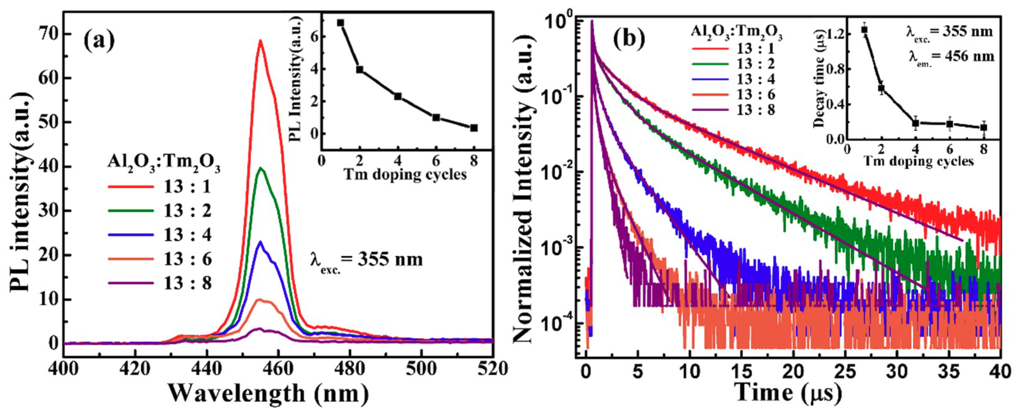
The Tm2O3 films deposited by ALD can be crystalized into Tm2O3 phase even without annealing, while the Al2O3 films are amorphous after annealing at 800 °C. However, the nanolaminate Al2O3/Tm2O3 film with the highest Tm content (AOT-8) is amorphous after annealing at 800 °C, therefore the nanolaminate structure restricts the grain growth of the dopant Tm2O3 layers. Figure 1a shows the PL spectra from the nanolaminate Al2O3/Tm2O3 films. The PL peaks at 456 nm are attributed to the transition of 1D2→3F4 in Tm3+ ions [20,21,22]. The inset of Figure 1a presents the comparison of the PL intensities of all samples, which decrease with the Tm2O3 dopant layers. Due to the common cluttering characteristics of RE ions, with the increase of Tm content, the number of activated Tm3+ ions decreases and the cross relaxation between Tm3+ ions further reduce the radiative transitions [30,31]. For TRPL results shown in Figure 1b, the decay lifetime of these PL emissions from Tm3+ ions also decreases with the Tm content, which coincides with the PL intensities. The inset gives the fitting values of the PL decay lifetime, which are in the range of 0.13–1.25 μs. The PL decay lifetime decreases rapidly as the Tm dopant layers rise to 4. The cross relaxation and concentration quenching contribute to the nonradiative recombination and decrease the luminescence lifetime.
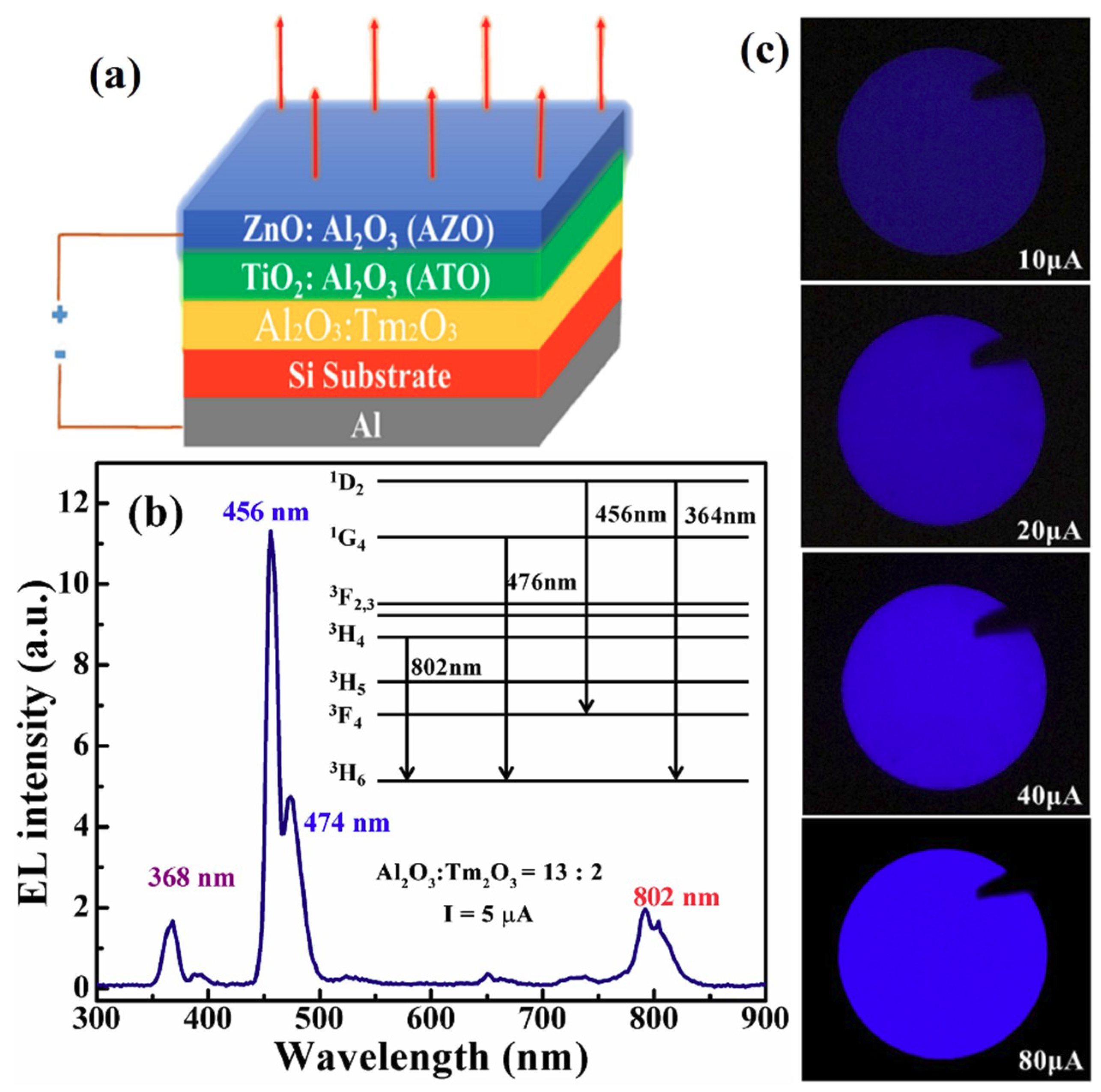
The schematic for the multilayered devices is shown in Figure 2a. The EL spectrum from the MOSLED based on the Al2O3/Tm2O3 nanolaminate with 2 cycles of Tm dopant (AOT-2) is presented in Figure 2b. The EL emissions mainly exhibit several peaks at the wavelengths of 368, 456, 474, and 802 nm, which originate from the radiative transitions from the 1D2, 3F4, 1G4, and 3H4 excited states to the 3H6 ground state in Tm3+ ions, respectively, as sketched in the inset of Figure 2b [21,22,23]. It is noteworthy that the EL emissions at 456 nm and 474 nm are dominating and the blue light is easily seen by naked eyes, as shown in Figure 2c. These images were taken by a digital camera from this AOT-2 MOSLED at different injection currents. The blue EL emission gradually brightens with the increase of the injection current from 10 µA to 80 µA.
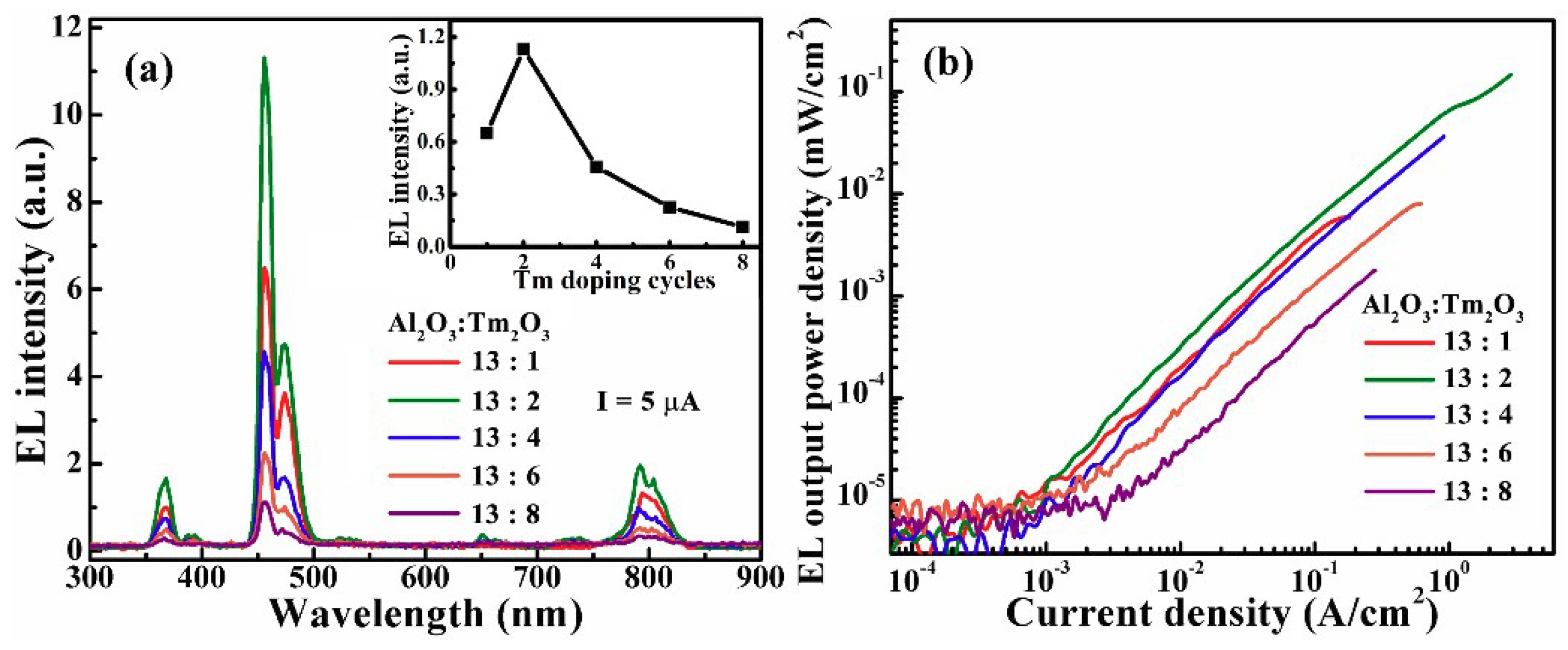
Figure 3a shows EL spectra from the MOSLEDs based on the Al2O3/Tm2O3 films with different Tm dopant cycles at an injection current of 5 µA. The concentrations of Tm dopant are from 0.69% to 4.95%, respectively. The spectra exhibit four peaks at 368, 458, 474, and 802 nm as mentioned above. The inset shows that the 456 nm blue EL intensity increases with the Tm dopant cycles up to 2 and then decreases due to concentration quenching. The EL presents higher tolerance for Tm clustering than the PL performance. The dependence of the 456 nm EL power density on the injection current density are shown in Figure 3b. Generally, the EL intensity presents a linear relationship with the injection current density. A power density up to 0.15 mW/cm2 was obtained from the optimal MOSLED at a current density of 2.87 A/cm2. Initially, the EL output power density increases as the Tm dopant cycles increases to 2, due to the increase of the excitable Tm3+ ions. The further decline of the power density with the Tm dopant cycle is attributed to the clustering and cross relaxation which reduce the number of excited Tm3+ ions [30,31]. The efficiency and output power are lower than the previously reported devices based on the Tb and Yb doped Al2O3 nanolaminates [18,19]. As the energy of the blue photon is higher than that of the green EL from Tb3+ ions and the near-infrared one from Yb3+ ions, the excitation possibility of the radiative transitions within Tm3+ ions should be lower which leads to the limited efficiency and output power. In addition, the visible EL from the RE-doped SiO2 is stronger than the devices in this work [32]. The higher working voltage needed for luminescence in SiO2 evidences the necessity of high electrical field for excitation of the photon with higher energy, which is adverse to practical application. However, this EL output power density is superior to the EL devices based on the RE-doped ZnO as the leakage current is greatly restricted comparatively [13].
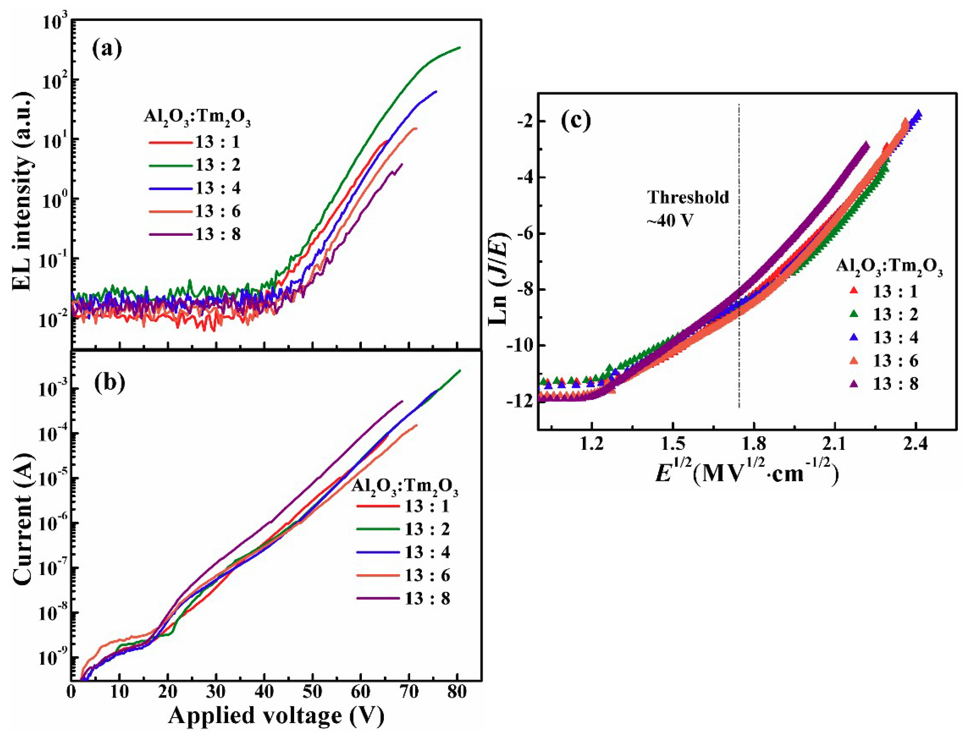
Figure 4a,b shows the dependence of blue (456 nm) EL intensities, together with the injection current, on the applied voltages for the nanolaminate MOSLEDs based on different Al2O3/Tm2O3 films. All devices exhibit a typical I–V characteristic of the MOS structure, i.e., the current starts with a low background one under the low electric field, then exponentially increases with the voltage [16,17,18,19]. The difference on the leakage currents mainly depends on the process of device procedures, coming from the electrons hopping through the defects within the matrix. At this stage, no hot electrons are generated in the Al2O3/Tm2O3 conduction band with no EL emissions. Afterwards, the injection current increases exponentially with the applied voltage and the conduction mechanism is dominated by the Poole–Franked (P–F) mode until the device breakdown [18,19]. In the P–F conduction mode the plot of the ln(J/E) versus E1/2 features a linear relationship (J is the current density and E is the electric field). As shown in Figure 4c, for all Al2O3/Tm2O3 MOSLEDs the P–F plots work in the EL-enabling voltages, with the threshold voltage of around 40 V (~3 MV/cm). The slopes of the linear plots of the P–F injections are similar while the little difference is caused by the slight variation of the injection current as mentioned above. Therefore, for the EL excitation, electrons are firstly injected into the conduction band of Al2O3 by trap-assisted tunneling and accelerated to gain energy under high electric field. These hot electrons excite the doped Tm3+ ions from the ground state to higher levels by inelastic collision. After the nonradiative relaxation, the radiative transitions in the Tm3+ ions from the excited state to ground state generate the characteristic EL emissions [20,21,22].
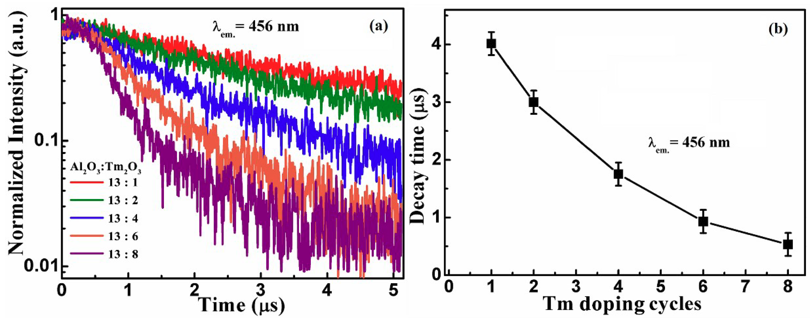
The EL decay lifetime of the 456 nm EL from different nanolaminate Al2O3/Tm2O3 MOSLEDs is measured under pulse excitation mode. The decay curves are shown in Figure 5a, which are close to the single exponential decay function. The decay lifetime decreases from 4.02 µs to 0.53 µs with the increase of Tm dopant cycles, as shown in Figure 5b. These values of EL decay lifetime are several times larger than that of PL decay lifetime shown in Figure 1b, and keep decreasing with the Tm doping concentration, which comes from the cross relaxation and concentration quenching caused by the excess Tm3+ ions. These phenomena again mean that the tolerance on the concentration quenching in EL performance is higher than that in PL.
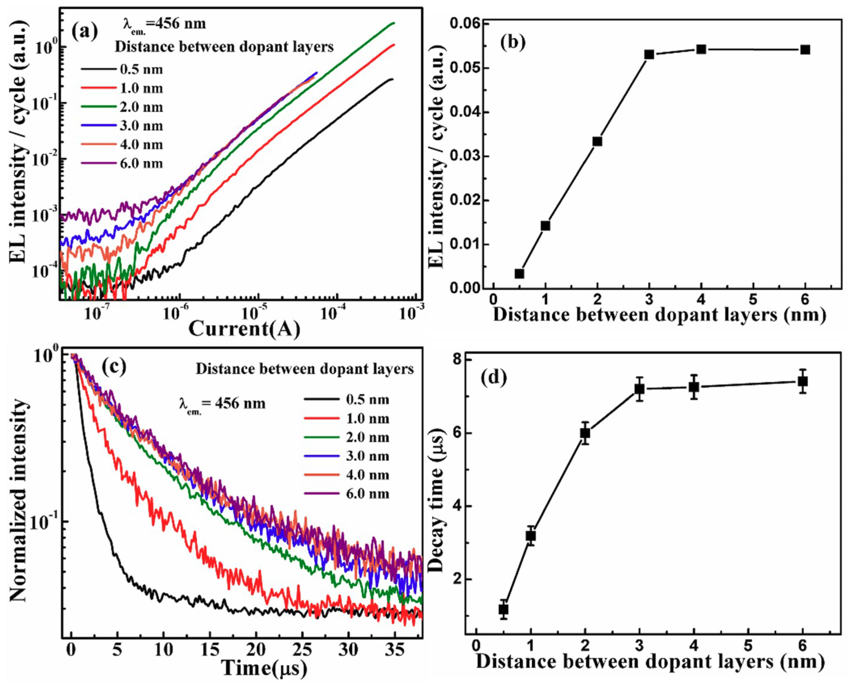
In the RE-doped Al2O3 MOSLEDs, the Al2O3 sublayer thickness affects the cross relaxation between excited RE ions, and the acceleration distance for injected electrons. In order to investigate the effect of the distance between Tm2O3 dopant layers, a series of MOSLEDs were fabricated in which the Al2O3 sublayer thickness varied from 0.5 nm to 6 nm while the Tm dopant cycles was fixed at 2. Figure 6a shows the dependence of the blue EL intensity on the injection current. Here, the EL intensities are divided by the cycle numbers to present the emissions from every Tm dopant cycle. With the increase of the thickness of Al2O3 sublayer, the contribution of a single Tm dopant cycle to the EL intensity firstly increases and then saturates as the Al2O3 interlayer thickness reaches 3 nm. Figure 6b presents the tendency. This phenomenon has been observed in our previous reports with a similar value, concerning the nonradiative interaction among excited RE3+ ions and the acceleration distance for the injected electrons [18,19]. Therefore, it is a common characteristic for the luminescent RE3+ ions in an Al2O3 matrix that the distance for the presence of nonradiative interaction and adequate electron acceleration is around 3 nm.
Furthermore, the decay lifetimes for these MOSLEDs are shown in Figure 6c, whose correlation with the Al2O3 interlayer thickness is summarized in Figure 6d. Similar to the EL intensity, the decay lifetime increases from 1.18 to 7.41 μs with the Al2O3 interlayer thickness increasing from 0.5 nm to 3 nm, and saturates at higher distances. The reduction of the decay lifetime at higher Tm doping concentrations is still ascribed to the increase of nonradiative cross relaxations between the two closely located Tm3+ dopant layers as mentioned above, with the similar critical Al2O3 interlayer thickness of 3 nm [19,33]. Considering the total EL intensities, the optimal Al2O3 interlayer thickness in these MOSLEDs is 2 nm. It should be noted that there is little difference between the total EL emission from nanolaminate Al2O3/Tm2O3 MOSLEDs with 1 nm and 2 nm Al2O3 interlayers. The effect of more dopant ions is offset by the relative lowered excitation efficiency. This optimal doping concentration is also consistent with previous reports (around 1 at%) on the RE doped luminescent materials [18,33].
The blue EL intensities (output powers) from our prototype devices are quite low and incapable of practical application. This work confirms the potential to realize blue EL from Al2O3/Tm2O3 nanolaminates by ALD. Moreover, the devices are fabricated entirely by ALD, which is characterized by the precise control of the film deposition over large substrates, and the compatibility with Si-based CMOS technology. Therefore, MOSLEDs based on Al2O3/Tm2O3 nanolaminates can be easily expanded for mass-production. The challenging deficiencies are the low EL efficiency and output power, the high working voltage, and the limited injection current. Further optimization can be achieved by adopting a thicker Al2O3/Tm2O3 luminescent layer with more optimal dopant structure and a less resistant protective layer with higher dielectric constant, to obtain a higher emission intensity.
4. Conclusions
Blue EL is demonstrated from nanolaminate Al2O3/Tm2O3 MOSLEDs fabricated by ALD. The emission at 456 nm from Tm3+ ions exhibits a power density of 0.15 mW/cm2. The decrease of the EL intensity and decay lifetime due to the clustering and cross-relaxation of the Tm3+ ions is observed by adjusting the Tm2O3 dopant cycles. The decay lifetime for the Tm3+ ions under optical excitation is in the range of 0.13–1.25 μs while under electrical excitation, the decay lifetime increases to 1.13–4.02 μs. The EL is attributed to the impact excitation of the Tm3+ ions by hot electrons in the Al2O3 matrix via the P–F mechanism. Consistent with the previous results, a critical Al2O3 interlayer thickness of ~3 nm for the nonradiative interaction among excited Tm3+ ions and the acceleration distance of the injected electrons works. This work could contribute to the development of Si-compatible RE-doped light sources by modifying the dopant structure in the nanolaminates to achieve efficient emissions.
Author Contributions
Conceptualization, J.S. and Y.Y.; methodology, Y.L. and Z.O.; validation, Y.L. and L.Y.; formal analysis, Y.L., Y.Y. and J.S.; writing—original draft preparation, Y.L.; writing—review and editing, Y.Y.; supervision, J.S.; funding acquisition, J.S. and Y.Y.
Funding
This research and APC were funded by National Natural Science Foundation of China, grant number 61674085 and 61705114, and China Postdoctoral Science Foundation, grant number 2017M611154.
Conflicts of Interest
The authors declare no conflict of interest.
References
- Gan, X.; Shiue, R.J.; Gao, Y.; Meric, I.; Heinz, T.F.; Shepard, K.; Hone, J.; Assefa, S.; Englund, D. Chip-integrated ultrafast graphene photodetector with high responsivity. Nat. Photonics 2013, 7, 883–887. [Google Scholar] [CrossRef] [Green Version]
- Marpaung, D.; Yao, J.; Capmany, J. Integrated microwave photonics. Nat. Photonics 2019, 13, 80–90. [Google Scholar] [CrossRef]
- Atabaki, A.; Moazeni, S.; Pavanello, F.; Gevorgyan, H.; Notaros, J.; Alloatti, L.; Wade, M.T.; Sun, C.; Kruger, S.A.; Meng, H.; et al. Integrating photonics with silicon nanoelectronics for the next generation of systems on a chip. Nature 2018, 556, 349–354. [Google Scholar] [CrossRef] [PubMed] [Green Version]
- Miritello, M.; Lo Savio, R.; Iacona, F.; Franzo, G.; Irrera, A.; Piro, A.M.; Bongiorno, C.; Priolo, F. Efficient luminescence and energy transfer in erbium silicate thin films. Adv. Mater. 2007, 19, 1582–1588. [Google Scholar] [CrossRef]
- Muravyev, S.V.; Anashkina, E.A.; Andrianov, A.V.; Dorofeev, V.; Motorin, S.E.; Koptev, M.Y. Dual-band Tm3+-doped tellurite fiber amplifier and laser at 1.9 μm and 2.3 μm. Sci. Rep. 2018, 8, 16164. [Google Scholar] [CrossRef] [PubMed]
- Nilsson, J.; Payne, D.N. High-Power Fiber Lasers. Science 2011, 332, 921–922. [Google Scholar] [CrossRef] [PubMed]
- Kim, J.H.; Holloway, P.H. Near-infrared-electroluminescent light-emitting planar optical sources based on gallium nitride doped with rare earths. Adv. Mater. 2005, 17, 91–96. [Google Scholar] [CrossRef]
- Irrera, A.; Franzo, G.; Iacona, F.; Canino, A.; Di Stefano, G.; Sanfilippo, D.; Piana, A.; Fallica, P.G.; Priolo, F. Light emitting devices based on silicon nanostructures. Physica E 2007, 38, 181–187. [Google Scholar] [CrossRef]
- Kenyon, A.J. Recent developments in rare-earth doped materials for optoelectronics. Prog. Quantum Electron. 2002, 26, 225–284. [Google Scholar] [CrossRef]
- Gu, L.L.; Xiong, Z.H.; Chen, G.; Xiao, Z.S.; Gong, D.W.; Hou, X.Y.; Wang, X. Luminescent erbium-doped porous silicon bilayer structures. Adv. Mater. 2001, 13, 1402–1405. [Google Scholar] [CrossRef]
- Eames, C.; Probert, M.I.J.; Tear, S.P. The structure and growth direction of rare earth silicide nanowires on Si(100). Appl. Phys. Lett. 2010, 96, 241903. [Google Scholar] [CrossRef]
- Tatebayashi, J.; Yoshii, G.; Nakajima, T.; Kamei, H.; Takatsu, J.; Lebrun, D.M.; Fujiwaraa, Y. Control of the energy transfer between Tm3+ and Yb3+ ions in Tm,Yb-codoped ZnO grown by sputtering-assisted metalorganic chemical vapor deposition. J. Appl. Phys. 2018, 123, 161409. [Google Scholar] [CrossRef]
- Yang, Y.; Li, Y.P.; Wang, C.X.; Zhu, C.; Lv, C.Y.; Ma, X.Y.; Yang, D.R. Rare earth doped ZnO films: A material platform to realize multicolor and near infrared electroluminescence. Adv. Opt. Mater. 2014, 2, 240–244. [Google Scholar] [CrossRef]
- Zhu, C.; Lv, C.Y.; Jiang, M.M.; Zhou, J.W.; Li, D.S.; Ma, X.Y.; Yang, D.R. Green electroluminescence from Tb4O7 films on silicon: Impact excitation of Tb3+ ions by hot carriers. Appl. Phys. Lett. 2016, 108, 051113. [Google Scholar] [CrossRef]
- Jambois, O.; Berencen, Y.; Hijazi, K.; Wojdak, M.; Kenyon, A.J.; Gourbilleau, F.; Rizk, R.; Garrido1, B. Current transport and electroluminescence mechanisms in thin SiO2 films containing Si nanocluster-sensitized erbium ions. J. Appl. Phys. 2009, 106, 063526. [Google Scholar] [CrossRef]
- Rebohle, L.; Braun, M.; Wutzler, R.; Liu, B.; Sun, J.M.; Helm, M.; Skorupa, W. Strong electroluminescence from SiO2-Tb2O3-Al2O3 mixed layers fabricated by atomic layer deposition. Appl. Phys. Lett. 2014, 104, 251113. [Google Scholar] [CrossRef]
- Sun, J.M.; Prucnal, S.; Skorupa, W.; Dekorsy, T.; Müchlich, A.; Helm, M.; Rebohle, L.; Gebel, T. Electroluminescence properties of the Gd3+ ultraviolet luminescent centers in SiO2 gate oxide layers. J. Appl. Phys. 2006, 99, 103102. [Google Scholar] [CrossRef]
- Ouyang, Z.; Yang, Y.; Sun, J. Near-infrared electroluminescence from atomic layer doped Al2O3:Yb nanolaminate films on silicon. Scr. Mater. 2018, 151, 1–5. [Google Scholar] [CrossRef]
- Yang, Y.; Li, N.; Sun, J.M. Intense electroluminescence from Al2O3/Tb2O3 nanolaminate films fabricated by atomic layer deposition on silicon. Opt. Express 2018, 26, 9344–9352. [Google Scholar] [CrossRef] [PubMed]
- Chen, Z.; Kang, S.; Zhang, H.; Wang, T.; Lv, S.; Chen, Q.; Dong, G.; Qiu, J. Controllable optical modulation of blue/green up-conversion fluorescence from Tm3+ (Er3+) single-doped glass ceramics upon two-step excitation of two-wavelengths. Sci. Rep. 2017, 7, 45650. [Google Scholar] [CrossRef] [PubMed]
- Lee, Y.W.; Chien, H.W.; Cho, C.H.; Chen, J.Z.; Chang, J.S.; Jiang, S. Heavily Tm3+-Doped Silicate Fiber for High-Gain Fiber Amplifiers. Fibers 2013, 1, 82–92. [Google Scholar] [CrossRef]
- Lee, D.S.; Steckl, A.J. Selective enhancement of blue electroluminescence from GaN:Tm. Appl. Phys. Lett. 2003, 82, 55–57. [Google Scholar] [CrossRef]
- Guereñu, A.L.; Bastian, P.; Wessig, P.; John, L.; Kumke, M.U. Energy Transfer between Tm-doped upconverting nanoparticles and a small organic dye with large stokes shift. Biosensors 2019, 9, 9. [Google Scholar] [CrossRef] [PubMed]
- Yamada, Y.; Kanemitsu, Y. Blue light emission from strongly photoexcited and electron-doped SrTiO3. J. Appl. Phys. 2011, 109, 102410. [Google Scholar] [CrossRef]
- Chawla, V.; Ruoho, M.; Weber, M.; Chaaya, A.A.; Taylor, A.A.; Charmette, C.; Miele, P.; Bechelany, M.; Michler, J.; Utke, I. Fracture mechanics and oxygen gas barrier properties of Al2O3/ZnO nanolaminates on PET deposited by atomic layer deposition. Nanomaterials 2019, 9, 88. [Google Scholar] [CrossRef] [PubMed]
- Bouriaux, L.F.; Rosamond, M.C.; Williams, D.A.; Davies, A.G.; Wälti, C. Field-enhanced direct tunneling in ultrathin atomic-layer-deposition-grown Au-Al2O3-Cr metal-insulator-metal structures. Phys. Rev. B 2017, 96, 115435. [Google Scholar] [CrossRef]
- Zhang, F.; Sun, G.; Zheng, L.; Liu, S.; Liu, B.; Dong, L.; Wang, L.; Zhao, W.; Liu, X.; Yan, G.; et al. Interfacial study and energy-band alignment of annealed Al2O3 films prepared by atomic layer deposition on 4H-SiC. J. Appl. Phys. 2013, 113, 044112. [Google Scholar] [CrossRef]
- Elam, J.W.; Routkevitch, D.; Mardilovich, P.P.; George, S.M. Conformal coating on ultrahigh-aspect-ratio nanopores of anodic alumina by atomic layer deposition. Chem. Mater. 2003, 15, 3507–3517. [Google Scholar] [CrossRef]
- Bosund, M.; Mizohata, K.; Hakkarainen, T.; Putkonen, M.; Söderlund, M.; Honkanen, S.; Lipsanen, H. Atomic layer deposition of ytterbium oxide using β-diketonate and ozone precursors. Appl. Surf. Sci. 2009, 256, 847–851. [Google Scholar] [CrossRef]
- Desirena, H.; De la Rosa, E.; Diaz-Torres, L.A.; Kumar, G.A. Concentration effect of Er3+ ion on the spectroscopic properties of Er3+ and Yb3+/Er3+ co-doped phosphate glasses. Opt. Mater. 2006, 28, 560–568. [Google Scholar] [CrossRef]
- Goldner, P.; Pellé, F. Size dependence of the luminescence spectra and dynamics of Eu3+: Y2O3 nanocrystals. J. Lumin. 1999, 83, 297–300. [Google Scholar]
- Sun, J.M.; Prucnal, S.; Skorupa, W.; Helm, M.; Rebohle, L.; Gebel, T. Increase of blue electroluminescence from Ce-doped SiO2 layers through sensitization by Gd3+ ions. Appl. Phys. Lett. 2006, 89, 091908. [Google Scholar] [CrossRef]
- Ouyang, Z.; Yang, Y.; Sun, J.M. Electroluminescent Yb2O3:Er and Yb2Si2O7:Er nanolaminate films fabricated by atomic layer deposition on silicon. Opt. Mater. 2018, 80, 209–215. [Google Scholar] [CrossRef]
Figure 1.
The (a) photoluminescence (PL) and (b) time-resolved photoluminescence (TRPL) spectra from the nanolaminate Al2O3/Tm2O3 films with different Tm dopant cycles excited by a 355 nm laser. The insets present the tendency of these PL intensities and PL decay lifetime with the Tm dopant cycles.
Figure 1.
The (a) photoluminescence (PL) and (b) time-resolved photoluminescence (TRPL) spectra from the nanolaminate Al2O3/Tm2O3 films with different Tm dopant cycles excited by a 355 nm laser. The insets present the tendency of these PL intensities and PL decay lifetime with the Tm dopant cycles.

Figure 2.
(a) The schematic for the luminescent devices based on the nanolaminate Al2O3/Tm2O3 films. (b) The EL spectrum from the device in which the Al2O3/Tm2O3 subcycle ratio is 13:2 (AOT-2), the inset shows the radiative transitions in the Tm3+ ions resulting in the EL emissions. (c) The images taken by a digital camera from this AOT-2 MOS-structured light-emitting device (MOSLED) at different injection currents.

Figure 3.
(a) EL spectra from the MOSLEDs based on the Al2O3/Tm2O3 films with different Tm dopant cycles at an injection current of 5 µA, the inset shows the tendency of this EL intensity with the Tm dopant layers. (b) The dependence of the 456 nm EL power density on the injection current density for the Al2O3/Tm2O3 MOSLEDs with different Tm dopant cycles.

Figure 4.
(a,b) The dependence of blue (456 nm) EL intensities, together with the injection current, on the applied voltages for the nanolaminate MOSLEDs based on different Al2O3/Tm2O3 films. (c) The plot of ln(J/E) versus E1/2 (Poole–Frenkel conduction mode) for these MOSLEDs.
Figure 4.
(a,b) The dependence of blue (456 nm) EL intensities, together with the injection current, on the applied voltages for the nanolaminate MOSLEDs based on different Al2O3/Tm2O3 films. (c) The plot of ln(J/E) versus E1/2 (Poole–Frenkel conduction mode) for these MOSLEDs.

Figure 5.
(a) The EL decay lifetime of the 456 nm EL from different nanolaminate Al2O3/Tm2O3 MOSLEDs and (b) the tendency of the EL decay lifetime with the Tm dopant cycles.
Figure 5.
(a) The EL decay lifetime of the 456 nm EL from different nanolaminate Al2O3/Tm2O3 MOSLEDs and (b) the tendency of the EL decay lifetime with the Tm dopant cycles.

Figure 6.
(a) The dependence of the blue EL intensity on the injection current from the Al2O3/Tm2O3 MOSLEDs with different Al2O3 sublayer thicknesses. Here, the EL intensities are divided by the cycle numbers to present the emissions from every Tm dopant cycle. (b) The relation of blue EL intensity with the Al2O3 sublayer thicknesses. (c) The EL decay lifetime for the Al2O3/Tm2O3 MOSLEDs and (d) the relation of lifetime to the Al2O3 sublayer thicknesses.


Table 1.
The corresponding experimental parameters for clarity.
| Sample Label | Tm3+ (at%) | Al2O3:Tm2O3 Cycle Number |
|---|---|---|
| AOT-1 | 0.69 | 13:1 |
| AOT-2 | 1.37 | 13:2 |
| AOT-4 | 2.64 | 13:4 |
| AOT-6 | 3.83 | 13:6 |
| AOT-8 | 4.95 | 13:8 |
| AOT-d05 | 2.46 | 7:2 |
| AOT-d1 | 1.37 | 13:2 |
| AOT-d2 | 0.69 | 26:2 |
| AOT-d3 | 0.45 | 40:2 |
| AOT-d4 | 0.35 | 52:2 |
| AOT-d6 | 0.23 | 78:2 |
© 2019 by the authors. Licensee MDPI, Basel, Switzerland. This article is an open access article distributed under the terms and conditions of the Creative Commons Attribution (CC BY) license (http://creativecommons.org/licenses/by/4.0/).
Share and Cite
MDPI and ACS Style
Liu, Y.; Ouyang, Z.; Yang, L.; Yang, Y.; Sun, J. Blue Electroluminescent Al2O3/Tm2O3 Nanolaminate Films Fabricated by Atomic Layer Deposition on Silicon. Nanomaterials 2019, 9, 413. https://doi.org/10.3390/nano9030413
AMA Style
Liu Y, Ouyang Z, Yang L, Yang Y, Sun J. Blue Electroluminescent Al2O3/Tm2O3 Nanolaminate Films Fabricated by Atomic Layer Deposition on Silicon. Nanomaterials. 2019; 9(3):413. https://doi.org/10.3390/nano9030413
Chicago/Turabian StyleLiu, Yao, Zhongtao Ouyang, Li Yang, Yang Yang, and Jiaming Sun. 2019. "Blue Electroluminescent Al2O3/Tm2O3 Nanolaminate Films Fabricated by Atomic Layer Deposition on Silicon" Nanomaterials 9, no. 3: 413. https://doi.org/10.3390/nano9030413
Note that from the first issue of 2016, this journal uses article numbers instead of page numbers. See further details here.