Article

Synthesis and Surface-Enhanced Raman Scattering of Ultrathin SnSe2 Nanoflakes by Chemical Vapor Deposition

1
School of Physics and Electronics, Shandong Normal University, Jinan 250014, China
2
Institute of Materials and Clean Energy, Shandong Normal University, Jinan 250014, China
*
Author to whom correspondence should be addressed.
Nanomaterials 2018, 8(7), 515; https://doi.org/10.3390/nano8070515
Submission received: 7 June 2018 / Revised: 2 July 2018 / Accepted: 6 July 2018 / Published: 10 July 2018

Abstract

:
As a new atomically layered, two-dimensional material, tin (IV) diselenide (SnSe2) has attracted extensive attention due to its compelling application in electronics and optoelectronics. However, the great challenge of impurities and the preparation of high-quality ultrathin SnSe2 nanoflakes has hindered far-reaching research and SnSe2 practical applications so far. Therefore, a facile chemical vapor deposition (CVD) method is employed to synthesize large-scale ultrathin SnSe2 flakes on mica substrates using SnSe and Se powder as precursors. The structural characteristics and crystalline quality of the product were investigated. Moreover, Raman characterizations indicate that the intensity of A1g peak and Eg peak, and the Raman shift of Eg are associated with the thickness of the SnSe2 nanoflakes. The ultrathin SnSe2 nanoflakes show a strong surface-enhanced Raman spectroscopy (SERS) activity for Rhodamine 6G (R6G) molecules. Theoretical explanations for the enhancement principle based on the chemical enhancement mechanism and charge transfer diagram between R6G and SnSe2 are provided. The results demonstrate that the ultrathin SnSe2 flakes are high-quality single crystal and can be exploited for microanalysis detection and optoelectronic application.
Keywords:
SnSe2; CVD; ultrathin; SERS

1. Introduction

Two-dimensional (2D) layered materials have received intensive attention owing to their superior properties in the field of photonics, electronics, and optoelectronics. The unique ultrathin 2D structure causes tunable band gaps and large specific surface areas [1,2,3]. Since graphene began to be explored [4], many 2D materials, such as transition metal sulfides (MoS2 [5,6], MoSe2 [7,8], and WSe2 [9,10]), III-VIA group semiconductors (GaS [11,12], InSe [13,14]), and IV-VIA group semiconductors (SnS2 [15,16]), have shown excellent performances in photodetectors [7], phototransistors [6], field effect transistors (FETs) [5], supercapacitor electrodes [17], and energy storage [18]. In recent decades, growing interest has focused on the exploration of 2D layered materials for potential usage in surface-enhanced Raman scattering [19]. Surface-enhanced Raman spectroscopy (SERS) is an important and powerful tool for the characterization of material structure. As a highly promising analytical tool, SERS plays an important role in ultrasensitive biomedical and chemical detection, which is very helpful for the potential application of chemical and biological sensing. The large specific surface area and specific structure have a tremendous influence on properties of 2D material. Accordingly, it is a pressing matter to synthesize large-scale ultrathin 2D layered materials and explore its Raman enhancement effect for further research.
Tin (IV) selenide (SnSe2), as a momentous material of the IV-VIA group, crystallizes with a hexagonal crystal structure in space group P-3m1 of the CdI2-type, in which the Sn–Se–Sn sandwich layered structure is formed by strong covalent forces in plane and weak van der Waals interaction dominates out of plane [20,21]. SnSe2 is a potential candidate for anodes for lithium-ion batteries [22], solar cells [23], supercapacitors [24], optoelectronic devices [25], and phase change memory [26] because of its appropriate indirect band gap (theoretical value of 0.71 eV in bulk material and 0.969 eV monolayer material). Moreover, both Sn and Se elements are earth-abundant and environmentally friendly, which further makes 2D SnSe2 a potential candidate for optoelectronics.
Exfoliation in bulk is an easy and convenient method to obtain single- or few-layered thin film for the most 2D layered materials, such as MoS2, graphene, and SnSe2 [20,27]. However, the exfoliated 2D material has limited applications due to poor control in size and low yield. Some other synthetic methods, such as hydrothermal synthesis [28,29], molecular beam epitaxy [30], and chemical vapor deposition (CVD) [25,31,32] have also been used for the synthesis of layered material. Among them, the CVD method has been proposed as an important and successful method to synthesize various single-crystalline ultrathin layered 2D materials, such as MoSe2, WSe2, and their heterostructures, due to the advantages of high yield and high crystal quality [33]. Motivated by this, He et al. reported the shape evolution of SnSe2 nanoflakes on SiO2/Si substrate via CVD employing Se and SnSe powder as precursors with the thinnest approximately 10 nm [25]. Then, Zhai et al. synthesized SnSe2 nanoflakes via CVD employing Se and SnI2 powder as precursors [21]. However, there are some inherent problems with this method, such as the use of tin sources which introduce new impurities. Therefore, more improvements are required to acquire large-scale, high-quality SnSe2 for practical applications.
In this work, we have successfully synthesized large-scale ultrathin SnSe2 nanoflakes of high quality on mica substrates employing Se and SnSe powder as precursors. SnSe with an appropriate melting point as a tin source does not introduce new impurities and guarantees the synthesis of ultrathin SnSe2 nanoflakes. Mica was selected as a substrate to guarantee the growth of SnSe2 along the horizontal orientation. Argon was used as the transfer gas to ensure the safety of the experiment. The lateral dimension of the nanoflakes is about 10 μm, and the layer number mainly varies from a monolayer to dozens of layers. In particular, various shapes of SnSe2, such as hexagonal, truncated triangular, and triangular were synthesized. Optical microscopy (OM), scanning electron microscopy (SEM), energy dispersive X-ray spectroscopy (EDX), transmission electron microscopy (TEM), X-ray photoelectron spectroscopy (XPS), X-ray diffraction (XRD), and atomic force microscopy (AFM) were employed to characterize the crystal quality, composition and crystal structures of the SnSe2 nanoflakes. Then, we further study the Raman peak change of sample with the decrease of thickness, and the Raman enhancement of SnSe2 on Rhodamine 6G (R6G) molecules. The ultrathin SnSe2 shows an excellent SERS activity for R6G, and the enhancement effect is explained by the principle of charge transfer.

2. Experimental Section

2.1. Synthesis of the SnSe2 Nanoflakes

The synthesis of the SnSe2 nanoflakes was carried out in a horizontal one-zone tube furnace (Lindberg/Blue M, TF55035KC-1, Thermo scientific, Asheville, NC, USA) with a silica tube (in a diameter of 1 inch and length of 20 inches) by CVD method. During the typical growth process, a high-purity Se powder (99.9% Alfa) (in one quartz boat) of 20 mg was placed at about 13.5 cm away from the center of the furnace and 10 mg of SnSe powder (99.9% Alfa) (in another quartz boat) was placed at the center of the furnace. Prior to the experiment, the two quartz boats were ultrasonically cleaned with acetone, ethanol and deionized water. Freshly cleaved mica substrate (10 mm × 20 mm Changchun Taiyuan Fluorphlogopite Co. Ltd., Changchun, China) was placed downstream of the tube furnace, and the distance between the mica and the center of the tube furnace was 13 cm. The temperature of the central zone increased from room temperature to 600 °C in 12 min to reduce chemical reactions during heating. The growth process lasted 5 min at a total pressure of 120 Torr and an argon atmosphere of 30 standard cubic centimeters per minute (sccm). Once the reaction was achieved, the lid of the furnace was open immediately for the purpose of cooling. Triangular truncated, triangular and hexagonal SnSe2 nanoflakes were deposited on the mica substrate.

2.2. Characterization of SnSe2 Nanoflakes

The morphology and size of as-synthesized SnSe2 flakes were characterized by an OM (Axio Observer. A1m, Zeiss, Oberkochen, Germany) and SEM (Sigma 500, Zeiss, Oberkochen, Germany). An AFM (Dimension Icon, Bruker, Karlsruhe, Germany) was used to measure the morphology and thickness of the SnSe2 flakes. The crystalline structure and composition of the SnSe2 were investigated by adopting XRD, XPS, TEM, and EDX. TEM, High-resolution TEM imaging, and selected area electron diffraction (SAED) (JEM-2100, Japan Electron Optics Laboratory Co. Ltd., Tokyo, Japan) measurements were performed on the TEM grid by transferring with poly(methyl methacrylate) (PMMA) method. An EDX (XFlash 6130, Bruker, Berlin, Germany) was used to characterize element ratio and uniformity. The information of binding energies in SnSe2 was characterized by employing an XPS (Escalab 250, Thermo Fisher scientific, Waltham, MA, USA) to verify the presence of Sn and Se. Crystal faces were identified and scanned by using an XRD (EPMA-1600, ShimaDu, Tokyo, Japan) with the angular range of 2θ from 10° to 80°. Raman spectra were recorded in a confocal Raman system (HR Evolution, Horiba, Paris, France) with a 532 nm laser, the laser spot was ~1 μm and the powder on the sample surface was kept below 0.5 mw to avoid any heating effects. Raman mapping was collected by a confocal Raman system with a laser wavelength of 532 nm and scanning step intervals of 1 μm.

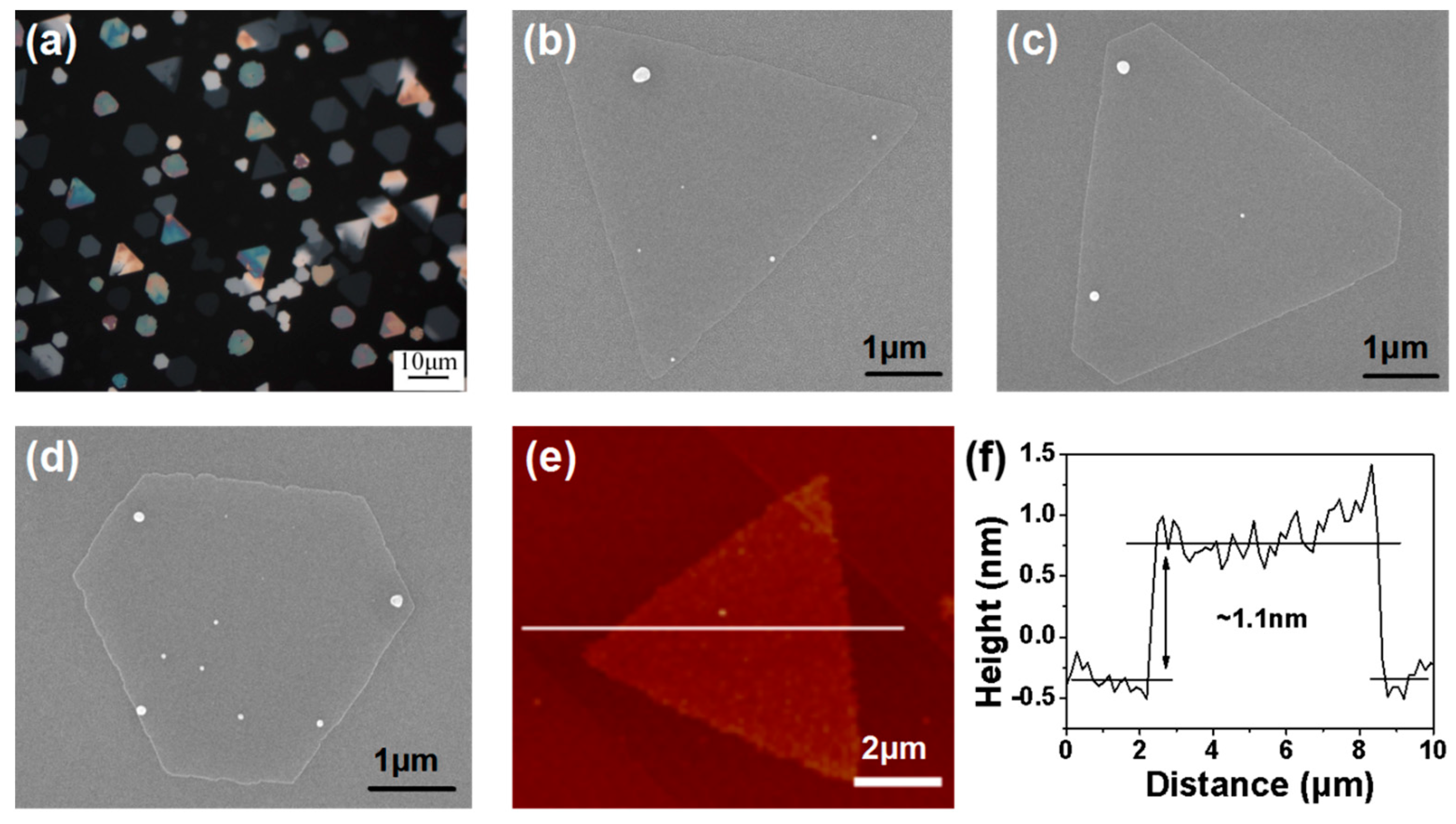
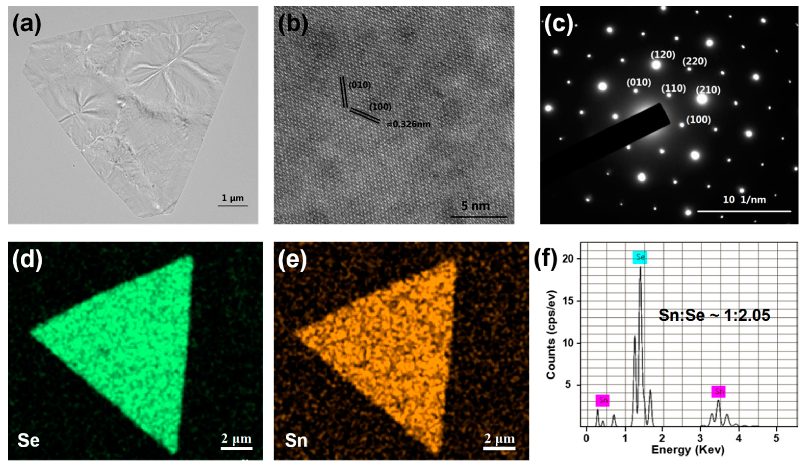
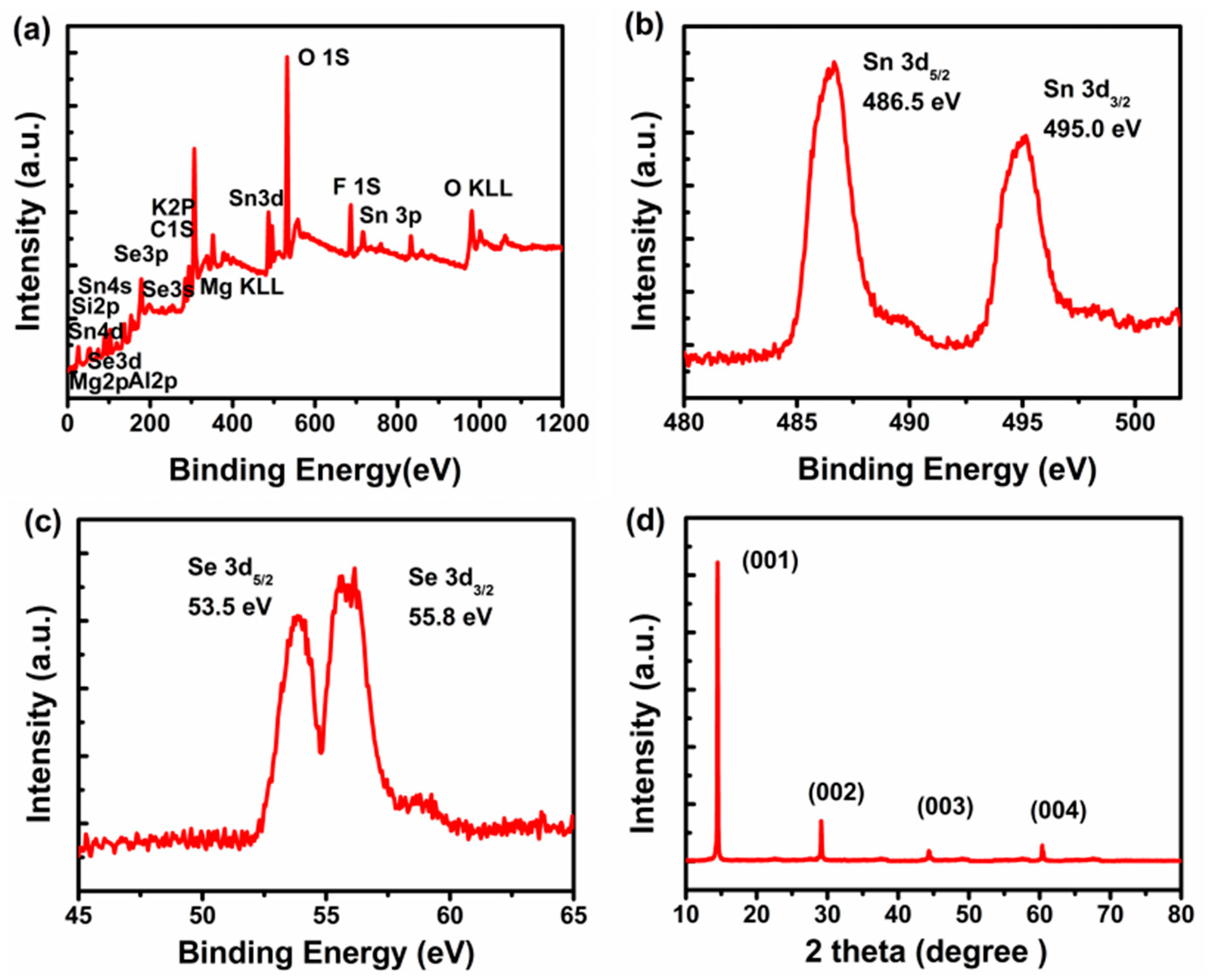
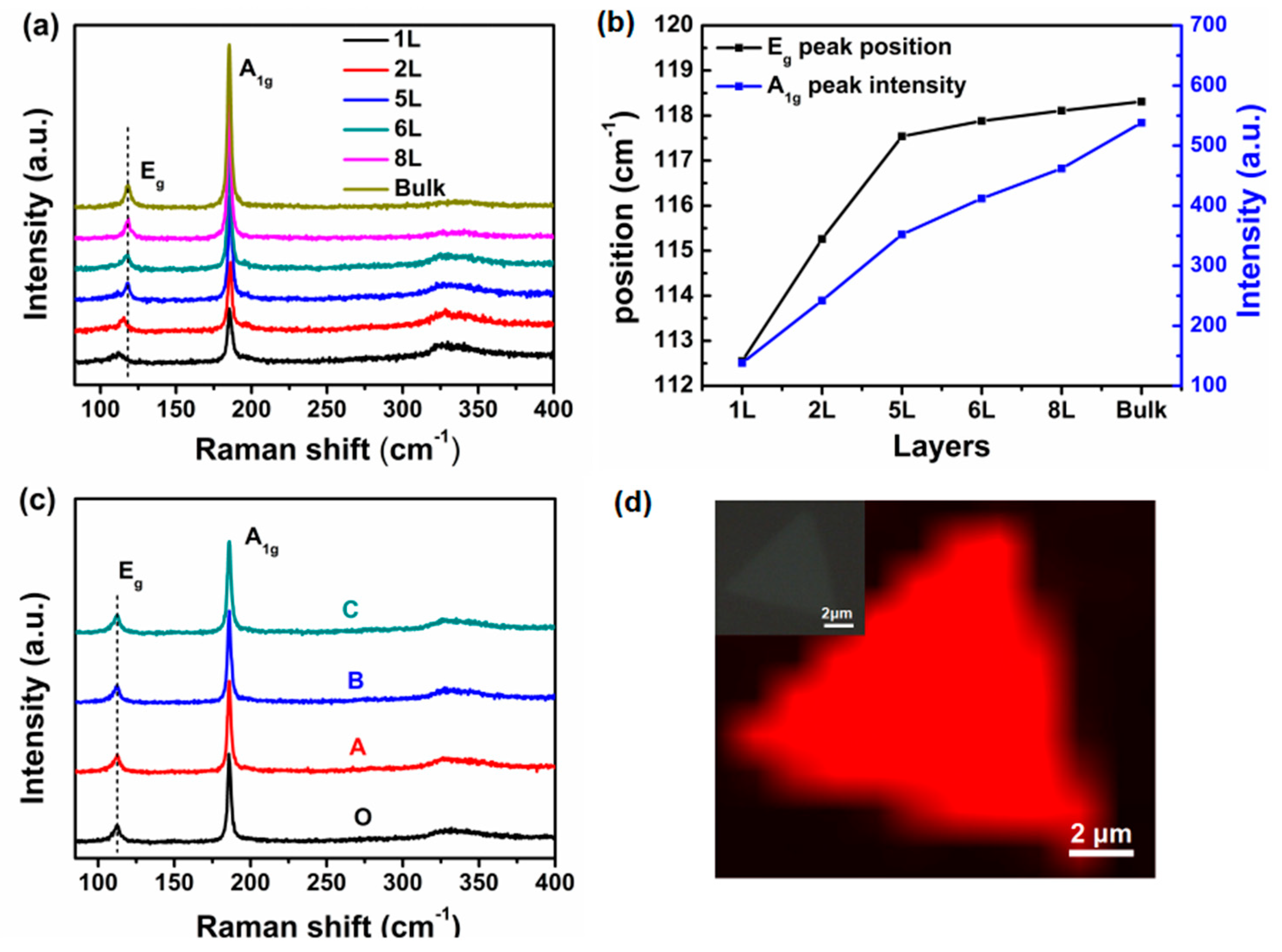
3. Results and Discussions

Typically, ultrathin SnSe2 nanoflakes were synthesized on mica substrates at 600 °C with Ar (30 sccm) flows under the pressure of 120 Torr via CVD method (for more details see the Experimental Section). In the process of growth, SnSe and Se powder, used as precursors, were put in the two different quartz boats, respectively. In comparison with other sources, such as SnO2 SnI2 and Sn, SnSe was used as Sn source because its proper melting point (861 °C) guaranteed slow evaporation during the growth process. Moreover, the two precursors do not contain other elements of SnSe2, resulting in new impurities [32]. In addition, fluorophlogopite mica was utilized as the substrate for growing 2D materials due to its chemical inertness and atomically smooth surface [34]. Furthermore, SnSe2 grown on mica substrate was expected to obtain in-plane flakes due to mica having the van der Waals substrate (graphene, SnSe2, etc.), which could freely release the strain energy [16].
OM, SEM, and AFM were used to measure the morphology of the SnSe2 nanoflakes grown by CVD method. Figure 1a shows a typical optical image of large-scale and ultrathin SnSe2 flakes with lateral lengths of about 10 µm. Moreover, large-scale optical images show a high-yield of SnSe2 nanoflakes (Figure S1, Supporting Information). The images show that SnSe2 nanoflakes with different shapes including hexagonal, truncated triangular, and triangular, are distributed on the mica substrates. The shape evolution of SnSe2 nanoflakes may be slightly different from the ratio of elements [25]. Nanoflakes with different thicknesses observed by OM showed slightly different colors. To sum up, thinner SnSe2 nanoflakes have darker color (dark), and thicker nanoflakes have brighter color (white) [35]. The color contrast indicates that the thickness of the SnSe2 nanoflakes varies slightly between different nanoflakes. The magnified SEM images (Figure 1b–d) show that the SnSe2 samples have regular shapes and smooth surfaces except for some points. The thicknesses of the SnSe2 nanoflakes were further characterized by AFM. The AFM image (Figure 1e) and the corresponding step height profile curve (Figure 1f) of a SnSe2 nanoflake reveals a relatively flat surface with a thickness of about 1.1 nm, such thickness corresponds to monolayers [20]. More height measurements demonstrate that the thickness of the SnSe2 nanoflakes is mainly between 1.1 nm to 10 nm (Figure S2, Supporting Information).
The crystal quality of the SnSe2 nanoflake was characterized by TEM and the selected area electron diffraction (SAED) pattern. The SnSe2 samples were transferred to a TEM grid with the help of poly(methyl methacrylate) (PMMA) [36]. Figure 2a shows a low-magnification TEM image of a representative SnSe2 nanoflake. The invariant of the transferred sample indicates the high-quality SnSe2 produced by CVD growth. Contrast SEM images, the samples observed with TEM under the same magnification have folds, indicating that folds are caused during the transfer and drying process [37]. The corresponding high-resolution TEM (HRTEM) image (Figure 2b) shows obvious lattice fringe, and the lattice spacing of 0.326 nm is in accordance with the (100) interplanar distance of the SnSe2, and the perfect lattice fringe suggests the high-quality of our samples [29]. Moreover, the SAED pattern is presented in Figure 2c, showing the hexagonal crystalline of SnSe2, clearly reveals a six-fold symmetry similar to other 2D layered materials, such as MoS2 [38,39]. These results indicate that our SnSe2 is a hexagonal high-quality single crystal. To further identify the composition and uniformity of the sample, we employed the EDX mapping, shown in Figure 2d,e, to explore the uniformity of spatial distribution of Se and Sn elements across the whole SnSe2 nanoflake. In addition, the corresponding EDX spectrum of the SnSe2 nanoflake is shown in Figure 2f. The atomic ratio of Se and Sn is about 2:1, coinciding well with the element ratio of SnSe2. These characterization data indicate that the product is highly crystalline SnSe2 crystal without impurities.
The chemical compositions and bonding types of the SnSe2 nanoflakes grown on mica by CVD method were examined with XPS. It provides the information on stoichiometry and bonding of samples. Eight elements are present in the spectra shown in Figure 3a. Sn and Se elements come from the SnSe2 nanoflakes, and others come from the mica (KMg3(AlSi3O10)F2) substrate. The 3d spectra of the SnSe2 samples (Figure 3b,c) have Sn3d3/2, Sn3d5/2, Se3d3/2, and Se3d5/2 peaks which can be observed at 495.0 eV, 486.5 eV, 55.8 eV and 53.5 eV, respectively [40]. Sn3d3/2 and Sn3d5/2 characteristic peaks are situated at 495.0 and 486.5 eV, respectively, certifying that tin is in its Sn (IV) state [41,42]. The binding energies of 55.8 and 53.5 eV are attributed to the doublet Se3d3/2 and Se3d5/2 peaks corresponding to the −2 state of Selenium, which coincides with the values of the previous work [43]. The characteristic peaks of tin indicate that the valence state of Sn changes from Sn2+ to Sn4+ [42]. The peaks of Se at about 55 eV were split into Se3d5/2 (53.5 eV) and Se3d3/2 (55.8 eV) [43]. The XPS further suggests that the products are SnSe2 without other impurities, such as SnSe.
XRD patterns were characterized to elucidate the overall crystallinity on a mica substrate. The XRD pattern obtained from SnSe2 nanoflakes is shown in Figure 3d. The XRD pattern of as-synthesized crystal is very consistent with the characteristic peaks of standard SnSe2. The prominent peaks at 2θ values of 14°, 29°, 44.2°, and 60°, correspond to the (001), (002), (003), and (004) planes of SnSe2, respectively [29,31,41]. This shows that the SnSe2 has a hexagonal lattice structure. The most obvious peak is located at 2θ = 14°, corresponding to the (001) crystal plane, revealing that the SnSe2 crystal grain preferentially grows along the c-axis. In addition, the obtained nanoflakes have a hexagonal lattice with the lattice constant a = b = 0.38 nm and c = 0.614 nm that agrees with the JCPDSN 89-2939 for the referred SnSe2 crystal. In brief, the XRD patterns coincide with the literature data of the characteristic peaks of SnSe2 crystal and prove that the as-grown products are made up of SnSe2.
Raman spectra were employed to investigate the crystal structure of the as-synthesized SnSe2 nanoflakes thoroughly. As far as we know, the peak of SnSe2 in about 185 cm−1 is assigned to out-plane vibrational A1g mode; in the light of the Eg peak position, tin selenide can be divided into two different polytypes: 2H and 1T. For the 2H-SnSe2 crystal, the Eg mode is located at 108 cm−1 approximately. For the 1T-SnSe2 crystal, the Eg mode gives rise to a band at 118 cm−1 [44]. As we observed in Figure 4a, the Raman spectra of the SnSe2 nanoflakes show a distinct identification of 1T-SnSe2 Raman spectra. With the decrease in thickness, the Eg peak becomes inconspicuous due to the reduction in the number of scattering centers in the ultrathin SnSe2 nanoflakes, which is in agreement with the previous literature [45]. The change of Eg peak position with the thickness of SnSe2 is shown in Figure 4b, in which an obvious redshift is observed. The wavenumber of the Eg mode decreases slightly from 118.3 cm−1 to 112.6 cm−1 with the reduction in the layer number, which can be attributable to surface effects and inter- and intralayer couplings [46]. The intensity of out-plane vibration mode (A1g) decreases remarkably as the thickness decreases, which is likely induced by the mechanical properties of the SnSe2 nanoflakes. For 2D layered material, the layers are coupled together by van der Waals forces. With the increase of the layer number, the van der Waals forces increase quickly, which can be reflected by the variation of Young’s modulus of crystalline 2D flakes [37]. The increase of out-plane vibration will influence the corresponding Raman intensity. This phenomenon, perhaps, provides an easy way to judge the number of the SnSe2 layers on mica substrates. In addition, the Raman spectra (Figure 4c) of four different points from a SnSe2 nanoflake show the identical feature of 1T-phase, revealing the homogeneity of the as-grown SnSe2 (Figure S3, Supporting Information). Moreover, Raman intensity mapping of the A1g mode of the typical SnSe2 nanoflakes at 185 cm−1 reveals a uniform intensity over the whole flake (Figure 4d). Moreover, the Raman peaks of SnSe have not been found [25], indicating that high purity SnSe2 is successfully synthesized via the improved CVD method.
In a word, the synthesis of high-quality SnSe2 was obtained by using mica substrate and SnSe source. SnSe with an appropriate melting point is beneficial to the synthesis of ultrathin SnSe2 and does not introduce new impurities. As a van der Waals substrate, mica is propitious to the horizontal growth of the crystal. Simultaneously, the tube furnace was heated to 600 °C in 12 min to reduce the reaction of the source during the heating process. The pressure was maintained at 120 Torr to ensure the formation of ultrathin samples. The pressure was too high to grow into a thicker sample, as shown in Figure S4. Argon was used as transmission gas, which is convenient to operate and ensures the safety of the experiment. Then, the characterizations of the morphology and structure of the samples indicate that the as-grown SnSe2 is a pure phase, high-quality, single crystal.
To prove the potential application in microanalytics and optoelectronics, SERS effect of R6G molecules on the different thicknesses of SnSe2 was analyzed. Herein, the main vibrations of R6G molecule are confirmed according to the previous article [47]. As shown in Figure 5a, the two strong vibration modes of 614 and 776 cm−1 are due to vibronic coupling between R6G molecules and SnSe2; the four high-frequency vibration modes are caused by the stretching of aromatic C–C; the remaining two modes are attributable to the combination of the four stretching modes. The Raman spectra of R6G molecules on SnSe2 with different layers are shown in Figure 5a. The Raman spectral peaks of R6G on monolayer SnSe2 were significantly higher than the other layers of SnSe2. All identifiable vibration modes of R6G decrease with the increase in the number of SnSe2 layers. Two vibrational peaks at 1185 and 1306 cm−1 disappear until R6G molecules are deposited on eight layers of SnSe2, which is probably because the two vibration modes are relatively weak. The relationship between R6G signal intensity and thickness of SnSe2 indicates that the thickness of the SnSe2 seriously affects SERS activities. To explore the enhanced ability of different thicknesses of SnSe2 substrates, the linear fitted curve of the relationship between the number of SnSe2 layers and the intensity of the peak at 614 cm−1 is presented in Figure 5c. A linear response with a high coefficient of determination (R2: 0.993) is achieved. In addition, SERS measurements were carried out under different concentrations of R6G molecules (Figure 5b). The Raman intensity value of the vibrational peak at 1363 cm−1 of R6G with 10−6 M concentration taken for SnSe2 substrate is larger than those obtained for R6G on other substrates, such as WSe2, Graphene, MoS2 (about 2.5-, 2.5-, and 10-fold higher than WSe2, Graphene, and MoS2, respectively) [48]. These results may be due to the lower quantum yield collected from other materials compared with that obtained from SnSe2. When the concentration of R6G is as low as 10−7 M, the Raman peaks (614, 776, 1185, 1306, 1363, 1506, 1575, and 1650 cm−1) are still conspicuous. Specifically, when the concentration of R6G is lowered to 10−8 M, the vibrational peak at 614 cm−1 still exists because of the existence of strong vibronic coupling between SnSe2 and R6G molecules. Herein, we investigated the relationship between the intensity of 614 cm−1 peak and the R6G concentration. The consummate linear response of the SnSe2/mica substrate with the high determination coefficient (R2: 0.990) in log scale is shown in Figure 5d. In general, these results demonstrate that the as-synthesized SnSe2 has a strong effect on the R6G molecule and expand the application of SnSe2 to microanalysis and microdetection.
For the Raman enhancement mechanism, the electromagnetic mechanism (EM) and chemical mechanism (CM) are two widely accepted mechanisms [49]. EM is mainly due to the enhancement of the local electromagnetic field caused by light-excited surface plasmons resonance. The EM mechanism requires the surface of the substrates to be rough and, therefore, generate surface plasmons resonance. CM is caused by photoinduced charge transfer between the target molecule and substrate. During the charge transfer process, the polarizability of molecules increases, which effectively enhances the recombination of electrons and holes as well as the Raman scattering intensity. Furthermore, the CM mechanism requires a smooth surface and the Fermi level of the substrate is located between the highest occupied molecular orbit (HOMO) and the lowest unoccupied molecular orbit (LUMO). Charge transfer is able to happen from the substrate to the molecule or vice versa. After careful consideration of the specific surface area and relatively smooth surface of 2D SnSe2, the CM between the SnSe2 and the R6G molecule is evaluated.
Scheme 1 describes the charge-transfer process at the interface between R6G target molecule and SnSe2 substrate. As a traditional SERS probe, for R6G molecules, the HOMO is at −5.70 eV, and LUMO is at −3.40 eV. The valence band (VB) (−5.05 eV) and conduction band (CB) (−4.95 eV) of SnSe2 are located between the HOMO and LUMO. The vibronic coupling between SnSe2 (CB state |S> and VB state |S′>) and R6G molecule (excited state |K> and ground state |I>) leads to the charge transfer process. With consideration of the excitation energy and R6G molecule, when we use a laser with a laser wavelength of 532 nm, the following transfer processes can occur according to the energy level relationship: (1) (TS′S), (2) (TIK), (3) (TS′K), (4) (TIS), (5) (TIS′) and (6) (TSK) which are in shown in Scheme 1. These enormously enhance the polarizability of the R6G molecule and result in an increase in recombination of electrons and holes, and then enhance the peak intensity of R6G molecules. As a result of the CM mechanism, charge transfer is most likely to occur between the R6G molecule and a layer of SnSe2 that is in contact with molecules [50]. With the increase in the number of SnSe2 layers, the enhancement effect becomes weaker which can be associated with the band gap. The theoretical energy band gap values of SnSe2 [20] show that the band gap becomes larger with the reduction of thickness, which may lead to a decrease in the chemical potential difference between R6G molecule and SnSe2 and then the increase of the charge transfer. In brief, these results prove that the Raman enhancement mechanism in the SnSe2 is basically related to the charge transfer theory given the energy band structure.

4. Conclusions

In summary, we report the growth of large-scale, high-quality, ultrathin SnSe2 flakes on mica substrates via an improved chemical vapor deposition. The typical final product shows triangular, truncated triangular and hexagonal shapes with lateral size ranging from a few microns to a dozen microns and its smallest thickness of ~1.1 nm (monolayer). A variety of detailed characterization demonstrated that the synthesized SnSe2 flakes were high-quality, single crystals with the growth orientation along c-axis. Moreover, Raman spectra of the SnSe2 flakes of different thickness reveal that an obvious redshift for Eg mode with the reduction of the layer number but with no change for A1g mode. Furthermore, we investigated the SERS of R6G molecules on SnSe2 flakes, and this phenomenon was explained based on the principle of charge transfer. We have demonstrated that the as-synthesized SnSe2 is a promising 2D material in microanalysis filed.

Supplementary Materials

The following are available online at https://www.mdpi.com/2079-4991/8/7/515/s1, Figure S1: Large-scale optical images of the as-synthesized SnSe2 nanoflakes, Figure S2: AFM images of SnSe2 nanoflakes with different thickness. The insets show the corresponding height profiles, Figure S3: The Raman optical image of triangular nanoflakes, The Raman spectra corresponding to four positions are found in Figure 4c, Figure S4: SEM image of SnSe2 nanoflakes in higher pressure.

Author Contributions

M.L. and Y.Z. conceived and performed the experiments; Y.S., M.W. and K.Z. analyzed the data; B.M. contributed analysis tools; M.L. and Y.Z. wrote the paper.

Funding

This research was funded by [the Shandong Provincial Natural Science Foundation] grant number [ZR2018MA040] and [the National Natural Science Foundation of China] grant number [61307120, 11774208 and 11474187].

Conflicts of Interest

The authors declare no conflict of interest.

References

  1. Wang, Q.H.; Kalantar-Zadeh, K.; Kis, A.; Coleman, J.N.; Strano, M.S. Electronics and optoelectronics of two-dimensional transition metal dichalcogenides. Nat. Nanotechnol. 2012, 7, 699–712. [Google Scholar] [CrossRef] [PubMed] [Green Version]
  2. Mak, K.F.; Lee, C.; Hone, J.; Shan, J.; Heinz, T.F. Atomically thin MoS2: A new direct-gap semiconductor. Phys. Rev. Lett. 2010, 105, 136805. [Google Scholar] [CrossRef] [PubMed]
  3. Ji, Q.; Zhang, Y.; Zhang, Y.; Liu, Z. Chemical vapour deposition of group-VIB metal dichalcogenide monolayers: Engineered substrates from amorphous to single crystalline. Chem. Soc. Rev. 2015, 44, 2587–2602. [Google Scholar] [CrossRef] [PubMed]
  4. Novoselov, K.S.; Geim, A.K.; Morozov, S.V.; Jiang, D.; Zhang, Y.; Dubonos, S.V.; Grigorieva, I.V.; Firsov, A.A. Electric field effect in atomically thin carbon films. Science 2004, 306, 666–669. [Google Scholar] [CrossRef] [PubMed]
  5. Van der Zande, A.M.; Huang, P.Y.; Chenet, D.A.; Berkelbach, T.C.; You, Y.; Lee, G.H.; Heinz, T.F.; Reichman, D.R.; Muller, D.A.; Hone, J.C. Grains and grain boundaries in highly crystalline monolayer molybdenum disulphide. Nat. Mater. 2013, 12, 554–561. [Google Scholar] [CrossRef] [PubMed]
  6. Choi, W.; Cho, M.Y.; Konar, A.; Lee, J.H.; Cha, G.B.; Hong, S.C.; Kim, S.; Kim, J.; Jena, D.; Joo, J.; et al. High-detectivity multilayer MoS2 phototransistors with spectral response from ultraviolet to infrared. Adv. Mater. 2012, 24, 5832–5836. [Google Scholar] [CrossRef] [PubMed]
  7. Xia, J.; Huang, X.; Liu, L.Z.; Wang, M.; Wang, L.; Huang, B.; Zhu, D.D.; Li, J.J.; Gu, C.Z.; Meng, X.M. CVD synthesis of large-area, highly crystalline MoSe2 atomic layers on diverse substrates and application to photodetectors. Nanoscale 2014, 6, 8949–8955. [Google Scholar] [CrossRef] [PubMed]
  8. Baek, J.; Yin, D.; Liu, N.; Omkaram, I.; Jung, C.; Im, H.; Hong, S.; Kim, S.M.; Hong, Y.K.; Hur, J.; et al. Highly sensitive chemical gas detecting transistor based on highly crystalline CVD-grown MoSe2 films. Nano Res. 2016, 10, 1861–1871. [Google Scholar] [CrossRef]
  9. Gao, Y.; Hong, Y.-L.; Yin, L.-C.; Wu, Z.; Yang, Z.; Chen, M.-L.; Liu, Z.; Ma, T.; Sun, D.-M.; Ni, Z.; et al. Ultrafast growth of high-quality monolayer WSe2 on Au. Adv. Mater. 2017, 29, 1700990. [Google Scholar] [CrossRef] [PubMed]
  10. Huang, J.-K.; Pu, J.; Hsu, C.-L.; Chiu, M.-H.; Juang, Z.-Y.; Chang, Y.-H.; Chang, W.-H.; Iwasa, Y.; Takenobu, T.; Li, L.-J. Large-area synthesis of highly crystalline WSe2 monolayers and device applications. ACS Nano 2013, 8, 923–930. [Google Scholar] [CrossRef] [PubMed]
  11. Late, D.J.; Liu, B.; Luo, J.; Yan, A.; Matte, H.S.; Grayson, M.; Rao, C.N.; Dravid, V.P. GaS and GaSe ultrathin layer transistors. Adv. Mater. 2012, 24, 3549–3554. [Google Scholar] [CrossRef] [PubMed]
  12. Hu, P.; Wang, L.; Yoon, M.; Zhang, J.; Feng, W.; Wang, X.; Wen, Z.; Idrobo, J.C.; Miyamoto, Y.; Geohegan, D.B.; et al. Highly responsive ultrathin GaS nanosheet photodetectors on rigid and flexible substrates. Nano Lett. 2013, 13, 1649–1654. [Google Scholar] [CrossRef] [PubMed]
  13. Feng, W.; Zheng, W.; Cao, W.; Hu, P. Back gated multilayer InSe transistors with enhanced carrier mobilities via the suppression of carrier scattering from a dielectric interface. Adv. Mater. 2014, 26, 6587–6593. [Google Scholar] [CrossRef] [PubMed]
  14. Feng, W.; Wu, J.-B.; Li, X.; Zheng, W.; Zhou, X.; Xiao, K.; Cao, W.; Yang, B.; Idrobo, J.-C.; Basile, L.; et al. Ultrahigh photo-responsivity and detectivity in multilayer InSe nanosheets phototransistors with broadband response. J. Mater. Chem. C 2015, 3, 7022–7028. [Google Scholar] [CrossRef]
  15. Su, G.; Hadjiev, V.G.; Loya, P.E.; Zhang, J.; Lei, S.; Maharjan, S.; Dong, P.; P, M.A.; Lou, J.; Peng, H. Chemical vapor deposition of thin crystals of layered semiconductor SnS2 for fast photodetection application. Nano Lett. 2015, 15, 506–513. [Google Scholar] [CrossRef] [PubMed]
  16. Yang, D.; Li, B.; Hu, C.; Deng, H.; Dong, D.; Yang, X.; Qiao, K.; Yuan, S.; Song, H. Controllable growth orientation of SnS2 flakes for low-noise, high-photoswitching ratio, and ultrafast phototransistors. Adv. Opt. Mater. 2016, 4, 419–426. [Google Scholar] [CrossRef]
  17. Acerce, M.; Voiry, D.; Chhowalla, M. Metallic 1T phase MoS2 nanosheets as supercapacitor electrode materials. Nat. Nanotechnol. 2015, 10, 313–318. [Google Scholar] [CrossRef] [PubMed]
  18. Huang, X.; Zeng, Z.; Zhang, H. Metal dichalcogenide nanosheets: Preparation, properties and applications. Chem. Soc. Rev. 2013, 42, 1934–1946. [Google Scholar] [CrossRef] [PubMed]
  19. Fiori, G.; Bonaccorso, F.; Iannaccone, G.; Palacios, T.; Neumaier, D.; Seabaugh, A.; Banerjee, S.K.; Colombo, L. Electronics based on two-dimensional materials. Nat. Nanotechnol. 2014, 9, 768–779. [Google Scholar] [CrossRef] [PubMed]
  20. Yu, P.; Yu, X.; Lu, W.; Lin, H.; Sun, L.; Du, K.; Liu, F.; Fu, W.; Zeng, Q.; Shen, Z.; et al. Fast photoresponse from 1T tin diselenide atomic layers. Adv. Funct. Mater. 2016, 26, 137–145. [Google Scholar] [CrossRef]
  21. Zhou, X.; Gan, L.; Tian, W.; Zhang, Q.; Jin, S.; Li, H.; Bando, Y.; Golberg, D.; Zhai, T. Ultrathin SnSe2 flakes grown by chemical vapor deposition for high-performance photodetectors. Adv. Mater. 2015, 27, 8035–8041. [Google Scholar] [CrossRef] [PubMed]
  22. Choi, J.; Jin, J.; Jung, I.G.; Kim, J.M.; Kim, H.J.; Son, S.U. SnSe2 nanoplate-graphene composites as anode materials for lithium ion batteries. Chem. Commun. 2011, 47, 5241–5243. [Google Scholar] [CrossRef] [PubMed]
  23. Yu, X.; Zhu, J.; Zhang, Y.; Weng, J.; Hu, L.; Dai, S. SnSe2 quantum dot sensitized solar cells prepared employing molecular metal chalcogenide as precursors. Chem. Commun. 2012, 48, 3324–3326. [Google Scholar] [CrossRef] [PubMed]
  24. Zhang, C.; Yin, H.; Han, M.; Dai, Z.; Pang, H.; Zheng, Y.; Lan, Y.-Q.; Bao, J.; Zhu, J. Two-dimensional tin selenide nanostructures for flexible all-solid-state supercapacitors. ACS Nano 2014, 8, 3761–3770. [Google Scholar] [CrossRef] [PubMed]
  25. Huang, Y.; Xu, K.; Wang, Z.; Shifa, T.A.; Wang, Q.; Wang, F.; Jiang, C.; He, J. Designing the shape evolution of SnSe2 nanosheets and their optoelectronic properties. Nanoscale 2015, 7, 17375–17380. [Google Scholar] [CrossRef] [PubMed]
  26. Wang, R.Y.; Caldwell, M.A.; Jeyasingh, R.G.D.; Aloni, S.; Shelby, R.M.; Wong, H.S.P.; Milliron, D.J. Electronic and optical switching of solution-phase deposited SnSe2 phase change memory material. J. Appl. Phys. 2011, 109, 113506. [Google Scholar] [CrossRef]
  27. Zhou, W.; Yu, Z.; Song, H.; Fang, R.; Wu, Z.; Li, L.; Ni, Z.; Ren, W.; Wang, L.; Ruan, S. Lattice dynamics in monolayer and few-layer SnSe2. Phys. Rev. B 2017, 96. [Google Scholar] [CrossRef]
  28. Liu, K.; Liu, H.; Wang, J.; Feng, L. Synthesis and characterization of SnSe2 hexagonal nanoflakes. Mater. Lett. 2009, 63, 512–514. [Google Scholar] [CrossRef]
  29. Fang, Z.; Hao, S.; Long, L.; Fang, H.; Qiang, T.; Song, Y. The enhanced photoelectrochemical response of SnSe2 nanosheets. CrystEngComm 2014, 16, 2404–2410. [Google Scholar] [CrossRef]
  30. Park, Y.W.; Jerng, S.-K.; Jeon, J.H.; Roy, S.B.; Akbar, K.; Kim, J.; Sim, Y.; Seong, M.-J.; Kim, J.H.; Lee, Z.; et al. Molecular beam epitaxy of large-area SnSe2 with monolayer thickness fluctuation. 2D Mater. 2016, 4, 014006. [Google Scholar] [CrossRef]
  31. Wu, J.; Hu, Z.; Jin, Z.; Lei, S.; Guo, H.; Chatterjee, K.; Zhang, J.; Yang, Y.; Li, B.; Liu, Y.; et al. Spiral growth of SnSe2 crystals by chemical vapor deposition. Adv. Mater. Interfaces 2016, 3, 1600383. [Google Scholar] [CrossRef]
  32. Huang, L.; Yu, Y.; Li, C.; Cao, L. Substrate mediation in vapor deposition growth of layered chalcogenide nanoplates: A case study of SnSe2. J. Phys. Chem. C 2013, 117, 6469–6475. [Google Scholar] [CrossRef]
  33. Gong, Y.; Lei, S.; Ye, G.; Li, B.; He, Y.; Keyshar, K.; Zhang, X.; Wang, Q.; Lou, J.; Liu, Z.; et al. Two-step growth of two-dimensional WSe2/MoSe2 heterostructures. Nano Lett. 2015, 15, 6135–6141. [Google Scholar] [CrossRef] [PubMed]
  34. Peng, H.; Dang, W.; Cao, J.; Chen, Y.; Wu, D.; Zheng, W.; Li, H.; Shen, Z.X.; Liu, Z. Topological insulator nanostructures for near-infrared transparent flexible electrodes. Nat. Chem. 2012, 4, 281–286. [Google Scholar] [CrossRef] [PubMed]
  35. Hu, Y.; Chen, T.; Wang, X.; Ma, L.; Chen, R.; Zhu, H.; Yuan, X.; Yan, C.; Zhu, G.; Lv, H.; et al. Controlled growth and photoconductive properties of hexagonal SnS2 nanoflakes with mesa-shaped atomic steps. Nano Res. 2017, 10, 1434–1447. [Google Scholar] [CrossRef]
  36. Ma, D.; Shi, J.; Ji, Q.; Chen, K.; Yin, J.; Lin, Y.; Zhang, Y.; Liu, M.; Feng, Q.; Song, X.; et al. A universal etching-free transfer of MoS2 films for applications in photodetectors. Nano Res. 2015, 8, 3662–3672. [Google Scholar] [CrossRef]
  37. Sahabudeen, H.; Qi, H.; Glatz, B.A.; Tranca, D.; Dong, R.; Hou, Y.; Zhang, T.; Kuttner, C.; Lehnert, T.; Seifert, G.; et al. Wafer-sized multifunctional polyimine-based two-dimensional conjugated polymers with high mechanical stiffness. Nat. Commun. 2016, 7, 13461. [Google Scholar] [CrossRef] [PubMed] [Green Version]
  38. Lee, Y.H.; Zhang, X.Q.; Zhang, W.; Chang, M.T.; Lin, C.T.; Chang, K.D.; Yu, Y.C.; Wang, J.T.; Chang, C.S.; Li, L.J.; et al. Synthesis of large-area MoS2 atomic layers with chemical vapor deposition. Adv. Mater. 2012, 24, 2320–2325. [Google Scholar] [CrossRef] [PubMed]
  39. Zhan, Y.; Liu, Z.; Najmaei, S.; Ajayan, P.M.; Lou, J. Large-area vapor-phase growth and characterization of MoS2 atomic layers on a SiO2 substrate. Small 2012, 8, 966–971. [Google Scholar] [CrossRef] [PubMed]
  40. De Groot, C.H.; Gurnani, C.; Hector, A.L.; Huang, R.; Jura, M.; Levason, W.; Reid, G. Highly selective chemical vapor deposition of tin diselenide thin films onto patterned substrates via single source diselenoether precursors. Chem. Mater. 2012, 24, 4442–4449. [Google Scholar] [CrossRef]
  41. Saha, S.; Banik, A.; Biswas, K. Few-layer nanosheets of n-type SnSe2. Chem.-Eur. J. 2016, 22, 15634–15638. [Google Scholar] [CrossRef] [PubMed]
  42. Velicky, M.; Toth, P.S.; Rakowski, A.M.; Rooney, A.P.; Kozikov, A.; Woods, C.R.; Mishchenko, A.; Fumagalli, L.; Yin, J.; Zolyomi, V.; et al. Exfoliation of natural van der waals heterostructures to a single unit cell thickness. Nat. Commun. 2017, 8, 14410. [Google Scholar] [CrossRef] [PubMed]
  43. Harbec, J.Y.; Powell, B.M.; Jandl, S. Lattice dynamics of SnSe2. Phys. Rev. B 1983, 28, 7009–7013. [Google Scholar] [CrossRef]
  44. Smith, A.; Meek, P.; Liang, W. Raman scattering studies of SnS2 and SnSe2. J. Phys. C Solid State Phys. 1977, 10, 1321. [Google Scholar] [CrossRef]
  45. Hu, P.; Wen, Z.; Wang, L.; Tan, P.; Xiao, K. Synthesis of few-layer GaSe nanosheets for high performance photodetectors. ACS Nano 2012, 6, 5988–5994. [Google Scholar] [CrossRef] [PubMed]
  46. Lorchat, E.; Froehlicher, G.; Berciaud, S. Splitting of interlayer shear modes and photon energy dependent anisotropic Raman response in n-layer ReSe2 and ReS2. ACS Nano 2016, 10, 2752–2760. [Google Scholar] [CrossRef] [PubMed]
  47. Michaels, A.M.; Jiang, J.; Brus, L. Ag nanocrystal junctions as the site for surface-enhanced Raman scattering of single rhodamine 6G molecules. J. Phys. Chem. B 2000, 104, 11965–11971. [Google Scholar] [CrossRef]
  48. Lee, Y.; Kim, H.; Lee, J.; Yu, S.H.; Hwang, E.; Lee, C.; Ahn, J.-H.; Cho, J.H. Enhanced Raman scattering of rhodamine 6G films on two-dimensional transition metal dichalcogenides correlated to photoinduced charge transfer. Chem. Mater. 2015, 28, 180–187. [Google Scholar] [CrossRef]
  49. Campion, A.; Kambhampati, P. Surface-enhanced Raman scattering. Chem. Soc. Rev. 1998, 27, 241. [Google Scholar] [CrossRef]
  50. Ling, X.; Xie, L.; Fang, Y.; Xu, H.; Zhang, H.; Kong, J.; Dresselhaus, M.S.; Zhang, J.; Liu, Z. Can graphene be used as a substrate for Raman enhancement? Nano Lett. 2010, 10, 553–561. [Google Scholar] [CrossRef] [PubMed]
Figure 1. Morphology of as-synthesized atomic-layer SnSe2 nanoflakes. (a) Large-scale optical microscopy (OM) image of as-grown SnSe2 nanoflakes on mica to show high yield of SnSe2; Typical scanning electron microscopy (SEM) images of SnSe2 single crystal with (b) triangle; (c) truncated triangle, and (d) hexagon, respectively; (e) Atomic force microscopy (AFM) image of a typical SnSe2 nanoflake; (f) The height profile in (e) indicates that the SnSe2 nanoflakes are monolayer.
Nanomaterials 08 00515 g001
Figure 2. Transmission electron microscopy (TEM) and energy dispersive X-ray spectroscopy (EDX) characterization of SnSe2 nanoflakes. (a) Low-magnification TEM image of the typical SnSe2 nanoflake; (b) The corresponding high-resolution TEM image of the SnSe2 nanoflake in (a); (c) The selected area electron diffraction pattern of the SnSe2 single crystal; (d,e) The Se and Sn elemental mapping of the SnSe2 nanoflakes on mica, respectively; (f) EDS spectrum of the as-grown SnSe2 nanoflake on mica.
Nanomaterials 08 00515 g002
Figure 3. X-ray photoelectron spectroscopy (XPS) and X-ray diffraction (XRD) characterization of the SnSe2 crystal on mica. (a) The whole range of an XPS spectrum of the SnSe2; (b,c) XPS peak of Sn and Se elements in the SnSe2 crystal, respectively; (d) XRD pattern of the SnSe2 crystal.
Nanomaterials 08 00515 g003
Figure 4. Raman characterization of the SnSe2 nanoflakes. (a) Thickness-dependent Raman spectra of the as-synthesized SnSe2 nanoflakes on mica substrate; (b) The position of the Eg peak and the intensity of the A1g peak versus number of SnSe2 layers; (c) Raman spectra from four different positions of a triangular sample (corresponding Raman optical image in Figure S3); (d) Raman mapping of A1g mode of a typical triangular SnSe2 nanoflake. Inset: corresponding Raman optical image.
Nanomaterials 08 00515 g004
Figure 5. (a) Surface-enhanced Raman spectroscopy (SERS) spectra of 1 × 10⁻⁴ M Rhodamine 6G (R6G) molecule absorbed on different thickness SnSe2 nanoflakes; (b) SERS spectra of R6G with concentration from 10−4 to 10−8 M on monolayer SnSe2 nanoflakes; (c) The SERS intensity at 614 cm−1 of R6G as a function of the thickness of SnSe2 nanoflakes; (d) The intensity of SERS peak at 614 cm−1 of R6G changes as a function of the molecular concentration on the SnSe2/mica substrate. Laser wavelength: 532 nm; power: 0.5 mw; lens: 100 × objective; acquisition time: 8 s.
Nanomaterials 08 00515 g005
Scheme 1. Schematic energy diagram illustrating charge transfer process between R6G molecule and SnSe2 under the excitation of 532 nm.
Nanomaterials 08 00515 sch001

