Measuring the Density of States of the Inner and Outer Wall of Double-Walled Carbon Nanotubes
by
 and
and
Benjamin A. Chambers
1, 
Cameron J. Shearer
1,2,
LePing Yu
1,
Christopher T. Gibson
1,* and
and
Gunther G. Andersson
1,* 1
Flinders Centre for NanoScale Science and Technology, Flinders University, Adelaide SA 5001, Australia
2
Department of Chemistry, The University of Adelaide, Adelaide SA 5005, Australia
*
Authors to whom correspondence should be addressed.
Nanomaterials 2018, 8(6), 448; https://doi.org/10.3390/nano8060448
Submission received: 21 May 2018
/
Revised: 7 June 2018
/
Accepted: 14 June 2018
/
Published: 19 June 2018
(This article belongs to the Special Issue Applications of Carbon Nanotubes)
Abstract
:The combination of ultraviolet photoelectron spectroscopy and metastable helium induced electron spectroscopy is used to determine the density of states of the inner and outer coaxial carbon nanotubes. Ultraviolet photoelectron spectroscopy typically measures the density of states across the entire carbon nanotube, while metastable helium induced electron spectroscopy measures the density of states of the outermost layer alone. The use of double-walled carbon nanotubes in electronic devices allows for the outer wall to be functionalised whilst the inner wall remains defect free and the density of states is kept intact for electron transport. Separating the information of the inner and outer walls enables development of double-walled carbon nanotubes to be independent, such that the charge transport of the inner wall is maintained and confirmed whilst the outer wall is modified for functional purposes.
1. Introduction
Carbon nanotubes (CNTs) were observed as early as 1972 [1]; however, the first report of them was made by Iijima in 1991 [2]. CNTs consist of a varying number of coaxial tubes of graphite sheets from a single tube, known as a single-walled carbon nanotube (SWCNT), to many coaxial tubes classified as multiwalled carbon nanotubes (MWCNTs). CNTs are known for their electronic properties due to its sp2 bonding network, ranging from semiconducting to metallic behaviour with the possibility of electron transport without backscattering [3]. At present, three main methods are used to fabricate CNTs; chemical vapour deposition [4,5,6], arc discharge [1,7], and laser ablation [8]. The electronic structure of carbon nanotubes depends strongly on the production and purification methods as any surface modification, defects, or contamination will disrupt the sp2 network creating areas of sp3 hybridisation resulting in the degradation of the favourable electronic properties. Furthermore, the use of CNTs within an electronic device, or for application at an interface, typically requires functionalisation so they can be attached or fixed within a device. It has been shown that double-walled carbon nanotubes (DWCNTs) can be functionalised such that the outer wall of a DWCNT is defected; however, the inner wall is suggested to be protected sacrificially by the outer wall [9,10,11,12,13]. If the outside of a DWCNT has been modified for attachment, the inner tube is responsible for the electron transport within a device. It is therefore of interest to develop experimental techniques that enable the measurement of the valence electrons for both the inner and the outer walls of the CNTs such that one can optimise interfaces within electronic devices, such as tuning band gaps in solar cell junctions, supercapacitors, nanotransistors, or other semiconductor devices [14,15,16,17].
In the present work we aim to determine the density of states (DoS) of the inner and the outer wall of DWCNTs by applying electron spectroscopy. First, SWCNTs are measured using ultraviolet photoelectron spectroscopy (UPS) and metastable helium induced electron spectroscopy (MIES) to provide a reference using both methods for the same surface, which allows for a direct comparison of the instrumental techniques. Second, the DWCNTs will be examined with the separate methods providing electronic states of the inner and outer walls using UPS and the outer wall using MIES. This allows for a comparison of the DoS to determine the inner wall DoS. Raman spectroscopy has been applied to provide information regarding defects correlating with the observations of features in the DoS.
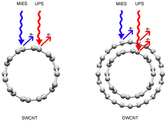
MIES is a surface sensitive valence electron spectroscopy technique, making it ideal to examine exclusively the electronic structure of the outer surface of materials like carbon nanotubes without contributions of the substrate [18]; or in the case of a DWCNT, the inner tube. The nature of the MIES measurement is determined by the interaction between the metastable Helium (He*) atoms and the sample, and results in the ejection of electrons measured by the spectrometer. This physical nature of the interaction is responsible for the perfect surface sensitivity.
Thus far, UPS has been applied to determine the valence electron structure of carbon nanotubes [19,20,21]. UPS has a probing depth of a few nm as a consequence of the mean free path of the excited electrons [22]. Thus, the probing depth of UPS exceeds the thickness of the outer wall of a CNT. Consequently, in UPS the superposition of the DoS of the multiple walls and substrate are detected. Therefore, it is almost impossible to separate in an UP spectrum the DoS contribution of the individual coaxial tubes and any contribution of the substrate.
Using a combination of ultraviolet photoelectron spectroscopy and metastable helium induced electron spectroscopy, the density of states of the inner and outer coaxial carbon nanotubes can be separated. When fabricating DWCNTs for use in electronic devices, the inner and outer walls have different purposes; the inner wall is responsible for charge transport whilst the outer wall is responsible for attachment or other functional reasons. Separating the characterisation of these coaxial tubes unlocks further refinement of fabricating DWCNTs for specific designs.
2. Materials and Methods
The SWCNTs were purchased from Carbon Solutions (P2-SWCNTs); purified with low functionality (i.e., the CNTs have a low number of functional groups), carbonaceous purity greater than 90% [23] and metal content less than 8 wt % from thermal gravimetric analysis in air. The DWCNTs were purchased from Sigma Aldrich (755141) with less than 10% metal content. The DWCNTs were treated for approximately 16 h in 3M HNO3 to dissolve any metal catalyst and amorphous carbon to match the purity of the P2-SWCNTs. The CNTs were suspended in N,N-dimethylformamide (Sigma-Aldrich, Castle Hill, Australia) and then filtered through 0.02 µm alumina filter (Whatman Anodisc, Bio-Strategy, Shanghai, China), which had previously been coated with 1 nm of chromium followed by 20 nm of gold using a magnetron sputter coating instrument (Q300T D, Quorum Technologies, East Sussex, UK). This allowed measurements of the CNTs without charging and without having to transfer to a different substrate.
The purity of the samples was verified with X-ray photoelectron spectroscopy (XPS) and Raman spectroscopy. XPS showed a composition of 97% C and 3% O and no impurities. The C 1s spectra were characteristic for sp2 hybridised C and are shown in the supplementary section in Figure S3. The C 1s spectra were similar to those published for highly oriented pyrolytic graphite (HOPG) [24]. Further, the Raman spectra were typical for SWCNTs and DWCNTs. No Raman spectra, corresponding to amorphous carbon, was observed for any sample indicating that the purity of the samples was sufficient for the present work.
The investigation of the CNTs was conducted using UPS in an ultra-high vacuum (UHV) system built by SPECS (Berlin, Germany) with a base pressure of a few 10−10 mbar. A two-stage cold cathode gas discharge from MFS (Claustal-Zellerfeld, Germany) was used to generate UV light (He I line) and metastable helium used for MIES (see below). The emitted electrons were detected via a hemispherical Phoibos 100 energy analyser from SPECS (Berlin, Germany). UPS was conducted with a pass energy of 10 eV. A bias of −10 V was applied to the samples for the UPS measurements. The angle of UV radiation and the analyser were 54° with respect to the sample normal.
UPS irradiated the sample with UV photons from the He I line (hν = 21.2 eV). The photons led to excitation of the valence electrons through the photoelectric effect. The surface sensitivity was limited by the electron mean free path to the upper 2–3 nm of the sample [22]. The binding energy of the electrons in the sample can be determined using Equation (1). Ekinetic is corrected for the bias of −10 V.
Ebinding = 21.2 eV − Ekinetic,
Instead of using electromagnetic radiation, one can use metastable helium atoms also produced by the cold cathode gas discharge used to create the UV light. When the metastable helium atom He* (1s2s) approaches the surface, two different pathways for de-excitation of the He* can occur [25]. The first mechanism is resonant ionisation (RI) followed by Auger neutralisation (AN). The second mechanism is Auger de-excitation (AD). The details of the MIES technique has been discussed in a previous paper [24,26].
Equation (1) holds also for spectra exclusively based on the AD mechanism but with an excitation energy of 19.8 eV instead of 21.2 eV. AD-based spectra were directly correlated to the DoS of the sample and can be plotted either against the kinetic energy or the binding energy of the emitted electrons. The measurements of the CNTs had sufficient AD contribution to allow for a comparison of the MIES and UPS on the binding energy scale [27]. MIES spectra taken at low temperatures ensure high AD-dominant spectra allowing for the direct comparison with UPS (see supplementary section, Figures S1 and S2). AN-dominated spectra have broader features than AD-dominated spectra [25,27].
Raman spectra were acquired using a WITec alpha 300R Raman microscope at an excitation laser wavelength of 532 nm with a ×40 objective (numerical aperture 0.60). Approximately 30 Raman spectra were recorded per sample at approximately 3 different areas. Each area was 100 × 100 µm in size and each region of the sample was separated by hundreds of microns. Typical integration times were 10–30 s for 2–3 accumulations per spectrum.
Each sample was heated in situ from room temperature to a high temperature of 733 K and held for approximately 10 min; this facilitates water desorption and the removal of adventitious carbon, which can result in large variations in the MIE and UP spectra [28]. A filament located under the sample holder was used for heating. The samples were each cooled using a gas line carrying nitrogen with a segment of a coil being submerged in liquid nitrogen. Temperatures of 113 and 173 K were achieved for the SWCNT and the DWCNT, respectively. Measurements of the surfaces were conducted with UPS and MIES before being measured with Raman spectroscopy.
3. Results
3.1. Raman Spectroscopy
Raman spectroscopy is extremely sensitive to repetitive network structure within CNTs. The sp2 network experiences planar vibrations resulting in Raman features around 1580 cm−1 annotated as G peaks [29]. Any defects or disorder in the structure will give rise to a D band approximately 1350 cm−1. A ratio of the intensity of the G and D peaks (G:D ratio) can be made to indicate, on average, the type of bonding the carbon atoms have within the repetitive structure and provide a value to quantify the order or disorder for different samples [30,31]. A radial breathing mode (RBM) band is also observed in Raman spectroscopy when looking at CNTs [32]. Due to its cylindrical nature, vibrations of the atoms on average will allow for contracted and expanded diameters giving a mechanism to estimate the diameter of the CNTs [33]. The Raman band just below 2700 cm−1 (~2680 cm−1) is an overtone of the D band and is commonly called the G’ band [34]. Like the RBM bands, the position of the G’ peak is related to the diameter of the nanotubes and the shape can also give an indication of whether a nanotube sample is single-walled or double-walled. For single-walled nanotubes the G’ band is typically a single symmetric peak, but for double-walled some broadening and asymmetry can potentially be observed. This is due to the inner and outer nanotubes in the double-walled nanotubes having different diameters [34]. It should also be noted that the nanotube diameter dependence is much weaker for the G’ band than for the RBM band [35].
Figure 1 (black line) is a single Raman spectrum of the SWCNT sample on the gold-chromium coated alumina substrate. The doublet within the G band is a characteristic of SWCNTs; the G− peak at 1570 cm−1 and the G+ peak at 1590 cm−1 [31,36]. The G:D ratio is 48.14 ± 14.19 (or, as is also used, the D:G ratio = 0.02 ± 0.006) indicating the surface is dominated by sp2 hybridisation. Figure 1 (red line) is a single Raman spectrum of the DWCNT sample on a gold-chromium coated alumina substrate. The D band for these DWCNTs is broader than the SWCNT and the G:D ratio is 5.294 ± 5.177 (or D:G ratio = 0.189 ± 0.185) giving evidence for the presence of defects with sp3 hybridisation. The radial breathing mode (RBM) for the SWCNT has a sharp peak focussed around 170 cm−1 whilst the DWCNT RBM is very broad, ranging from 65 to 290 cm−1.
Given the position of the RBM peak is inversely proportional to the diameter of the CNTs (Equation (2)), it can be estimated from the RBM peak that the diameter of the SWCNT is approximately 1.38 nm (using prefactor A = 234 cm−1 nm and assuming B = 0, i.e., negligible environmental effect) [32]. The DWCNT sample displayed a broad range of RBM, with peaks ranging from 65 to 290 cm−1, indicating diameters from 0.8 to 2.6 nm. This is consistent with observations by Moore et al. [37] with the peaks in the region near, and including, the 65 cm−1 band corresponding to the outer walls (up to a maximum of 2.6 nm) and the peaks in the region near, and including, the 290 cm−1 band corresponding to the inner walls (down to a minimum of 0.8 nm). This suggests that the DWCNT sample has a larger diameter distribution, with more RBM constituent peaks [37].
ωRBM = A/dt + B,
3.2. Analysis of Ultraviolet Photoelectron (UP) and Metastable Helium Induced Electron (MIE) Spectra
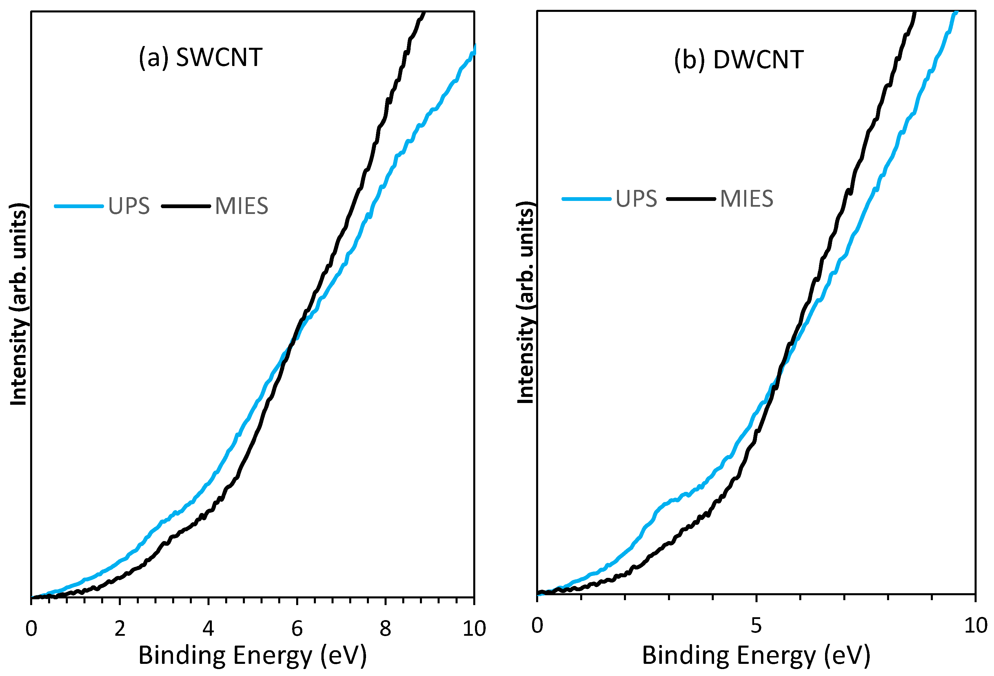
The UP and MIE spectra of SWCNTs (at 113 K) are presented in Figure 2a. Both the UP and the MIE spectra share the peak at 3 eV and a broad structure between 6 and 8 eV; the UPS has a peak evident at 8 eV. The 3 eV corresponds to the 2pπ states whilst the feature at between 6 and 8 eV relates to the 2pσ states [38,39].
The UP and MIE spectra for the DWCNTs (at 173 K) are presented in Figure 2b. The UP spectra, similar to the SWCNT, shows a feature at 3 eV corresponding to the 2pπ states [38,39] whilst the MIE spectra for DWCNTs seems to be depleted in the 3 eV region. The feature at 3 eV is specifically characteristic for the 2pπ states. It should be noted that the UP and MIE spectra for each of the SWCNTs and DWCNTs have been taken simultaneously, thus at the same temperature. The Raman results previously conducted on the DWCNTs indicated that the DWCNT sample had sp3 hybridisation and that the sp2 hybridisation is relatively low, thus the 2pπ states in the MIES would be low.
4. Discussion
UPS and MIES both examine the surface of the SWCNT and the DWCNT; however, due to the different interactions, MIES has a high surface sensitivity (only the outer most atoms) whilst UPS can penetrate a few nanometres, occasionally including the electron density of the substrate as well as the entire CNT cross-section. Reviewing the spectra in Figure 2b it could be stated that the MIE spectrum has indicated a limited population of 2pπ states on the outer layer of the DWCNT, supported by the Raman measurements, which indicated defects. The UP spectrum, however, still indicated a strong 2pπ signal similar to that seen in the SWCNT, which had very little defects. The UPS may be seeing the higher concentration of these states as it measures the inner tube within the DWCNT as well as the outside. It has previously been stated that the outer wall of a DWCNT is preferentially functionalised in a reaction leaving the inner wall DoS within the DWCNT intact; these measurements support this statement.
5. Conclusions
The UPS of DWCNTs provided information across the entire cross-section of the CNTs whilst the MIES provided information for the outer wall only. Combining the data from these two methods, the inner wall CNT valence electrons can be investigated, providing a better understanding of the internal electronic properties. This instrumental mechanism concluded that the DoS of the outer walls for the DWCNT was not favourable for use in electronic devices as it lost its ballistic conduction properties through possessing defects in the structure, however the inner wall of the DWCNT still maintained its population of low energy valence electrons desirable for ballistic conduction. This instrumental mechanism may also be considered for other materials composed of a few monolayers that experience different DoS at the outermost surface and immediately beneath the surface. The present work shows that combining surface analysis with MIES and UPS is specifically relevant for low-dimensional materials like CNTs and 2D materials.
Supplementary Materials
The following are available online at https://www.mdpi.com/2079-4991/8/6/448/s1, Figure S1: Comparison of MIES at range of temperatures (Kelvin); as the temperature drops the features amplify, Figure S2: Variation of AD and AN/RI dominance across the temperature range (Kelvin); AD dominates at lower temperatures, Figure S3: C 1s XP spectra of the SWCNT and DWCNT. The C1 s spectra are similar to those published for HOPG and characteristic for sp2 hybridised C.
Author Contributions
For research articles with several authors, a short paragraph specifying their individual contributions must be provided. The following statements should be used “Conceptualization, B.C. and G.A.; Methodology, B.C., G.A., C.G.; Validation, B.C., G.A., C.G., C.S., and L.Y.; Formal Analysis, B.C., G.A., and C.G.; Investigation, B.C., and C.G.; Resources, C.S. and L.Y.; Data Curation, B.C., G.A., and C.G.; Writing-Original Draft Preparation, B.C.; Writing-Review & Editing, B.C., G.A., and C.G.; Visualization, B.C.; Supervision, G.A.; Project Administration, G.A.; Funding Acquisition, G.A.”, please turn to the CRediT taxonomy for the term explanation. Authorship must be limited to those who have contributed substantially to the work reported.
Funding
This research received no external funding.
Acknowledgments
The authors acknowledge the expertise, equipment, and support provided by the Australian Microscopy and Microanalysis Research Facility (AMMRF) and the Australian National Fabrication Facility (ANFF) at Flinders University.
Conflicts of Interest
The authors declare no conflict of interest.
References
- Boehm, H.P. The first observation of carbon nanotubes. Carbon 1997, 35, 581–584. [Google Scholar] [CrossRef]
- Iijima, S. Helical microtubules of graphitic carbon. Nature 1991, 354, 56–58. [Google Scholar] [CrossRef]
- Ando, T. The electronic properties of graphene and carbon nanotubes. NPG Asia Mater. 2009, 1, 17–21. [Google Scholar] [CrossRef] [Green Version]
- Brukh, R.; Mitra, S. Mechanism of carbon nanotube growth by CVD. Chem. Phys. Lett. 2006, 424, 126–132. [Google Scholar] [CrossRef]
- Reddy, N.K.; Meunier, J.-L.; Coulombe, S. Growth of carbon nanotubes directly on a nickel surface by thermal CVD. Mater. Lett. 2006, 60, 3761–3765. [Google Scholar] [CrossRef]
- Baddour, C.E.; Fadlallah, F.; Nasuhoglu, D.; Mitra, R.; Vandsburger, L.; Meunier, J.-L. A simple thermal CVD method for carbon nanotube synthesis on stainless steel 304 without the addition of an external catalyst. Carbon 2009, 47, 313–318. [Google Scholar] [CrossRef]
- Ebbesen, T.W.; Ajayan, P.M. Large-scale synthesis of carbon nanotubes. Nature 1992, 358, 220–222. [Google Scholar] [CrossRef]
- Chrzanowska, J.; Hoffman, J.; Małolepszy, A.; Mazurkiewicz, M.; Kowalewski, T.A.; Szymanski, Z.; Stobinski, L. Synthesis of carbon nanotubes by the laser ablation method: Effect of laser wavelength. Phys. Status Solidi B 2015, 252, 1860–1867. [Google Scholar] [CrossRef] [Green Version]
- Muramatsu, H.; Kim, Y.A.; Hayashi, T.; Endo, M.; Yonemoto, A.; Arikai, H.; Okino, F.; Touhara, H. Fluorination of double-walled carbon nanotubes. Chem. Commun. 2005, 2002–2004. [Google Scholar] [CrossRef] [PubMed]
- Marcolongo, G.; Ruaro, G.; Gobbo, M.; Meneghetti, M. Amino acid functionalization of double-wall carbon nanotubes studied by Raman spectroscopy. Chem. Commun. 2007, 4925–4927. [Google Scholar] [CrossRef]
- Colomer, J.F.; Marega, R.; Traboulsi, H.; Meneghetti, M.; van Tendeloo, G.; Bonifazi, D. Microwave-Assisted Bromination of Double-Walled Carbon Nanotubes. Chem. Mater. 2009, 21, 4747–4749. [Google Scholar] [CrossRef]
- Hayashi, T.; Shimamoto, D.; Kim, Y.A.; Muramatsu, H.; Okino, F.; Touhara, H.; Shimada, T.; Miyauchi, Y.; Maruyama, S.; Terrones, M.; et al. Selective Optical Property Modification of Double-Walled Carbon Nanotubes by Fluorination. ACS Nano 2008, 2, 485–488. [Google Scholar] [CrossRef] [PubMed]
- Bulusheva, L.G.; Okotrub, A.V.; Flahaut, E.; Asanov, I.P.; Gevko, P.N.; Koroteev, V.O.; Fedoseeva, Y.V.; Yaya, A.; Ewels, C.P. Bromination of Double-Walled Carbon Nanotubes. Chem. Mater. 2012, 24, 2708–2715. [Google Scholar] [CrossRef]
- Yamashita, Y.; Yamamoto, S.; Mukai, K.; Yoshinobu, J.; Harada, Y.; Tokushima, T.; Takeuchi, T.; Takata, Y.; Shin, S.; Akagi, K.; et al. Direct observation of site-specific valence electronic structure at the SiO2/Si interface. Phys. Rev. B 2006, 73, 045336. [Google Scholar] [CrossRef]
- Chandra, A.; Andersona, G.; Melkote, S.; Gao, W.; Haitjema, H.; Wegener, K. Role of surfaces and interfaces in solar cell manufacturing. CIRP Ann. 2014, 63, 797–819. [Google Scholar] [CrossRef]
- Llinas, J.P.; Fairbrother, A.; Barin, G.B.; Shi, W.; Lee, K.; Wu, S.; Choi, B.Y.; Braganza, R.; Lear, J.; Kau, N.; et al. Short-channel field-effect transistors with 9-atom and 13-atom wide graphene nanoribbons. Nat. Commun. 2017, 8, 633. [Google Scholar] [CrossRef] [PubMed] [Green Version]
- Pan, H.; Li, J.; Feng, Y. Carbon Nanotubes for Supercapacitor. Nanoscale Res. Lett. 2010, 5, 654–668. [Google Scholar] [CrossRef] [PubMed]
- Morgner, H. The quantitative characterization of liquid and solid surfaces with metastable helium atoms. AIP Conf. Proc. 2000, 500, 687–698. [Google Scholar]
- Ayala, P.; Miyata, Y.; de Blauwe, K.; Shiozawa, H.; Feng, Y.; Yanagi, K.; Kramberger, C.; Silva, S.R.P.; Follath, R.; Kataura, H.; et al. Disentanglement of the electronic properties of metallicity-selected single-walled carbon nanotubes. Phys. Rev. B 2009, 80, 205427. [Google Scholar] [CrossRef]
- Kharlamova, M.V.; Sauer, M.; Saito, T.; Sato, Y.; Suenaga, K.; Pichler, T.; Shiozawa, H. Doping of single-walled carbon nanotubes controlled via chemical transformation of encapsulated nickelocene. Nanoscale 2015, 7, 1383–1391. [Google Scholar] [CrossRef] [PubMed] [Green Version]
- Wang, Y.-Q.; Sherwood, P.M.A. Studies of Carbon Nanotubes and Fluorinated Nanotubes by X-ray and Ultraviolet Photoelectron Spectroscopy. Chem. Mater. 2004, 16, 5427–5436. [Google Scholar] [CrossRef]
- Seah, M.P.; Dench, W.A. Quantitative electron spectroscopy of surfaces: A standard data base for electron inelastic mean free paths in solids. Surf. Interface Anal. 1979, 1, 2–11. [Google Scholar] [CrossRef]
- Itkis, M.E.; Perea, D.E.; Niyogi, S.; Rickard, S.M.; Hamon, M.A.; Hu, H.; Zhao, B.; Haddon, R.C. Purity Evaluation of As-Prepared Single-Walled Carbon Nanotube Soot by Use of Solution-Phase Near-IR Spectroscopy. Nano Lett. 2003, 3, 309–314. [Google Scholar] [CrossRef]
- Chambers, B.A.; Neumann, C.; Turchanin, A.; Gibson, C.T.; Andersson, G.G. The direct measurement of the electronic density of states of graphene using metastable induced electron spectroscopy. 2D Mater. 2017, 4, 025068. [Google Scholar] [CrossRef]
- Hagstrum, H.D. Excited-Atom Deexcitation Spectroscopy Using Incident Ions. Phys. Rev. Lett. 1979, 43, 1050–1053. [Google Scholar] [CrossRef]
- Ellis, A.V.; Al-deen, A.; Dalal, H.; Andersson, G.G. Structural Determination of Thermally and Hydrazine Treated Graphene Oxide Using Electron Spectroscopic Analysis. J. Phys. Chem. C 2013, 117, 21312–21319. [Google Scholar] [CrossRef]
- Morgner, H. The Characterization of Liquid and Solid Surfaces with Metastable Helium Atoms. In Advances in Atomic, Molecular, and Optical Physics; Benjamin, B., Herbert, W., Eds.; Academic Press: Cambridge, MA, USA, 2000; pp. 387–488. [Google Scholar]
- Chambers, B.A.; Notarianni, M.; Liu, J.; Motta, N.; Andersson, G.G. Examining the electrical and chemical properties of reduced graphene oxide with varying annealing temperatures in argon atmosphere. Appl. Surf. Sci. 2015, 356, 719–725. [Google Scholar] [CrossRef]
- Dresselhaus, M.S.; Jorio, A.; Saito, R. Characterizing Graphene, Graphite, and Carbon Nanotubes by Raman Spectroscopy. Annu. Rev. Condens. Matter Phys. 2010, 1, 89–108. [Google Scholar] [CrossRef] [Green Version]
- Yan, Y.; Cui, J.; Pötschke, P.; Voit, B. Dispersion of pristine single-walled carbon nanotubes using pyrene-capped polystyrene and its application for preparation of polystyrene matrix composites. Carbon 2010, 48, 2603–2612. [Google Scholar] [CrossRef]
- Dresselhaus, M.S.; Dresselhaus, G.; Saito, R.; Jorio, A. Raman spectroscopy of carbon nanotubes. Phys. Rep. 2005, 409, 47–99. [Google Scholar] [CrossRef]
- Araujo, P.T.; Maciel, I.O.; Pesce, P.B.C.; Pimenta, M.A.; Doorn, S.K.; Qian, H.; Hartschuh, A.; Steiner, M.; Grigorian, L.; Hata, K.; et al. Nature of the constant factor in the relation between radial breathing mode frequency and tube diameter for single-wall carbon nanotubes. Phys. Rev. B 2008, 77, 241403. [Google Scholar] [CrossRef] [Green Version]
- Dresselhaus, M.S.; Dresselhaus, G.; Jorio, A.; Filho, A.G.S.; Saito, R. Raman spectroscopy on isolated single wall carbon nanotubes. Carbon 2002, 40, 2043–2061. [Google Scholar] [CrossRef]
- Pfeiffer, R.; Kuzmany, H.; Simon, F.; Bokova, S.N.; Obraztsova, E. Resonance Raman scattering from phonon overtones in double-wall carbon nanotubes. Phys. Rev. B 2005, 71, 155409. [Google Scholar] [CrossRef]
- Souza Filho, A.G.; Jorio, A.; Samsonidze, G.G.; Dresselhaus, G.; Pimenta, M.A.; Dresselhaus, M.S.; Swan, A.K.; Ünlü, M.S.; Goldberg, B.B.; Saito, R. Competing spring constant versus double resonance effects on the properties of dispersive modes in isolated single-wall carbon nanotubes. Phys. Rev. B 2003, 67, 035427. [Google Scholar] [CrossRef]
- Jorio, A.; Fantini, C.; Dantas, M.S.S.; Pimenta, M.A.; Filho, A.G.S.; Samsonidze, G.G.; Brar, V.W.; Dresselhaus, G.; Dresselhaus, M.S.; Swan, A.K.; et al. Linewidth of the Raman features of individual single-wall carbon nanotubes. Phys. Rev. B 2002, 66, 115411. [Google Scholar] [CrossRef]
- Moore, K.E.; Flavel, B.S.; Ellis, A.V.; Shapter, J.G. Comparison of double-walled with single-walled carbon nanotube electrodes by electrochemistry. Carbon 2011, 49, 2639–2647. [Google Scholar] [CrossRef]
- Luo, Z.; Shang, J.; Lim, S.; Li, D.; Xiong, Q.; Shen, Z.; Lin, J.; Yu, T. Modulating the electronic structures of graphene by controllable hydrogenation. Appl. Phys. Lett. 2010, 97, 233111. [Google Scholar] [CrossRef]
- Bianconi, A.; Hagström, S.B.M.; Bachrach, R.Z. Photoemission studies of graphite high-energy conduction-band and valence-band states using soft-X-ray synchrotron radiation excitation. Phys. Rev. B 1977, 16, 5543–5548. [Google Scholar] [CrossRef]
Figure 1.
Raman spectra for a single-walled carbon nanotube (SWCNT) and a double-walled carbon nanotube (DWCNT) with inset showing the radial breathing mode (RBM) region.
Figure 1.
Raman spectra for a single-walled carbon nanotube (SWCNT) and a double-walled carbon nanotube (DWCNT) with inset showing the radial breathing mode (RBM) region.
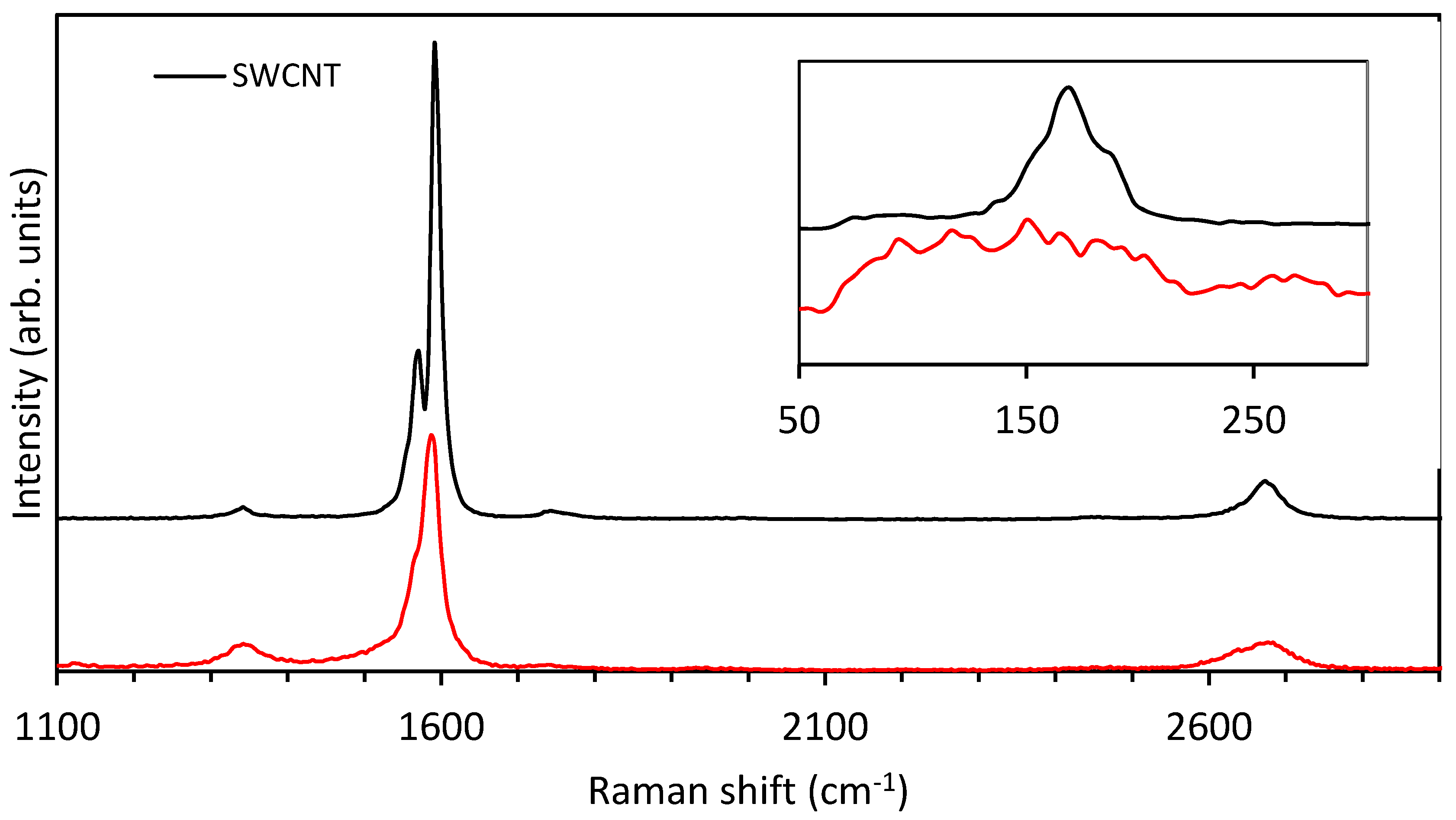
Figure 2.
Comparison of ultraviolet photoelectron (UP) and metastable helium induced electron (MIE) spectra at low temperatures for both (a) SWCNT (113 K) and (b) DWCNT (173 K).
Figure 2.
Comparison of ultraviolet photoelectron (UP) and metastable helium induced electron (MIE) spectra at low temperatures for both (a) SWCNT (113 K) and (b) DWCNT (173 K).

© 2018 by the authors. Licensee MDPI, Basel, Switzerland. This article is an open access article distributed under the terms and conditions of the Creative Commons Attribution (CC BY) license (http://creativecommons.org/licenses/by/4.0/).
Share and Cite
MDPI and ACS Style
Chambers, B.A.; Shearer, C.J.; Yu, L.; Gibson, C.T.; Andersson, G.G. Measuring the Density of States of the Inner and Outer Wall of Double-Walled Carbon Nanotubes. Nanomaterials 2018, 8, 448. https://doi.org/10.3390/nano8060448
AMA Style
Chambers BA, Shearer CJ, Yu L, Gibson CT, Andersson GG. Measuring the Density of States of the Inner and Outer Wall of Double-Walled Carbon Nanotubes. Nanomaterials. 2018; 8(6):448. https://doi.org/10.3390/nano8060448
Chicago/Turabian StyleChambers, Benjamin A., Cameron J. Shearer, LePing Yu, Christopher T. Gibson, and Gunther G. Andersson. 2018. "Measuring the Density of States of the Inner and Outer Wall of Double-Walled Carbon Nanotubes" Nanomaterials 8, no. 6: 448. https://doi.org/10.3390/nano8060448
Note that from the first issue of 2016, this journal uses article numbers instead of page numbers. See further details here.