Review of Fabrication Methods, Physical Properties, and Applications of Nanostructured Copper Oxides Formed via Electrochemical Oxidation


Abstract
:
1. Introduction
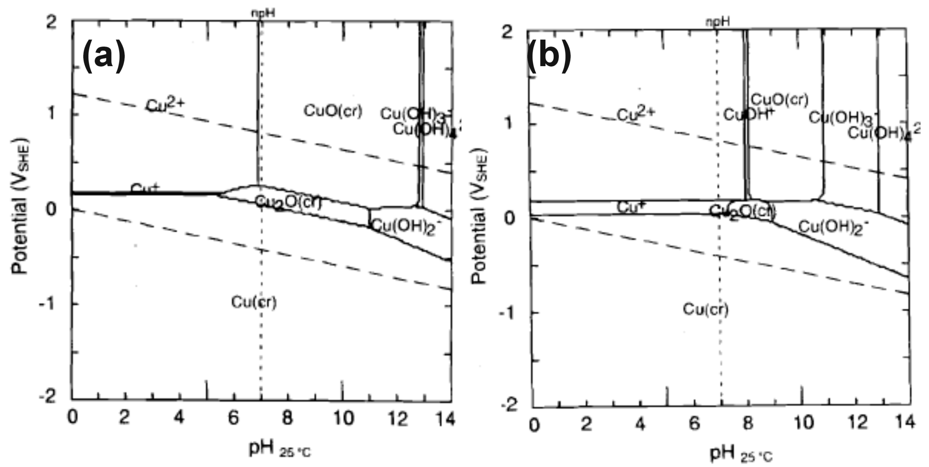
2. Passivation of Copper
3. Strategies of Copper Anodization
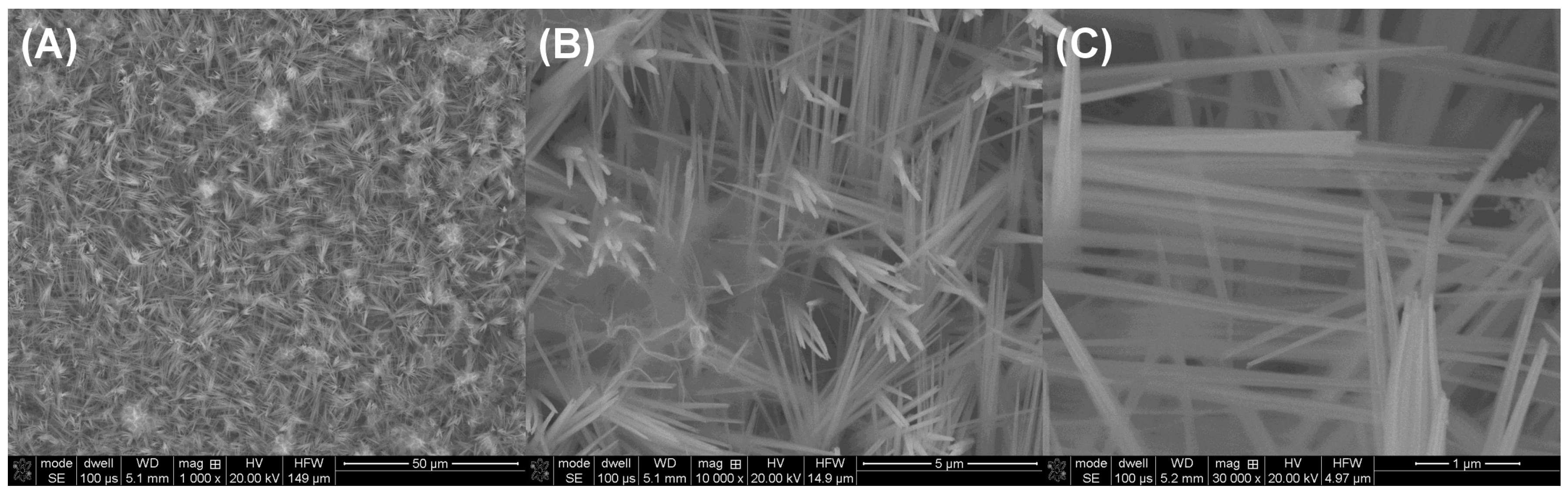
4. Properties and Applications of Anodic Nanostructures Grown on Copper
5. Anodization versus Other Nanostructured Copper Oxide Fabrication Methods
- It employs inexpensive equipment;
- It is time-efficient;
- It is an easy technique to scale-up, as it employs self-organization (no template required);
- It does not require numerous steps, only electropolishing and one step of the electrochemical oxidation;
- It allows for the control of geometry and provides 1D nanostructures with a high aspect ratio.
6. Conclusions and Challenges
- There are challenges in the formation of anodic copper oxides: generally, only KOH- and NaOH-based electrolytes were used for anodizing. The Pourbaix diagram revealed many more opportunities. Thus, electrolytes in a pH range from ca. 7 to 11 could provide different morphologies and more uniform chemical compositions. Potassium oxalate, used as an anodizing electrolyte, shows that there is still much to explore in this field.
- A full systemic study of the influence of the operating conditions (type of the electrolyte, voltage, time, temperature) on the morphology of the grown nanostructures has not yet been reported, though this would be beneficial for all researchers working in the field of applications of copper and cuprous oxide nanostructures. In this field, the formation of nanostructures via anodization with a diameter smaller than ca. 7 nm, in order to observe a significant QC effect, would be also challenging.
- There is also a demand to quantify the chemical composition of the grown nanostructures versus the operating conditions of anodization. It would be beneficial from both a fundamental point of view (understanding the mechanism of growth with hard, experimental data) and for applications in which chemical purity is crucial, such as photovoltaics.
- In contrast to all anodic oxides, nanostructures grown by copper electrochemical oxidation are crystalline. From a fundamental point of view, investigating the crystal orientation would be important, so as to determine whether the anodization of a planar sample, in a constant electric field, induces the growth of oriented, crystalline nanowires and nanoneedles.
Author Contributions
Acknowledgments
Conflicts of Interest
References
- Jani, A.M.M.; Losic, D.; Voelcker, N.H. Nanoporous anodic aluminium oxide: Advances in surface engineering and emerging applications. Prog. Mater. Sci. 2013, 58, 636–704. [Google Scholar] [CrossRef]
- Kowalski, D.; Kim, D.; Schmuki, P. TiO2 nanotubes, nanochannels and mesosponge: Self-organized formation and applications. Mater. Today 2013, 8, 235–264. [Google Scholar] [CrossRef]
- Wierzbicka, E.; Sulka, G.D. Fabrication of highly ordered nanoporous thin Au films and their application for electrochemical determination of epinephrine. Sens. Actuator B Chem. 2016, 222, 270–279. [Google Scholar] [CrossRef]
- Kumeria, T.; Rahman, M.M.; Santos, A.; Ferre-Borrull, J.; Marsal, L.F.; Losic, D. Nanoporous Anodic Alumina Rugate Filters for Sensing of Ionic Mercury: Toward Environmental Point-of-Analysis Systems. ACS Appl. Mater. Interfaces 2014, 6, 12971–12978. [Google Scholar] [CrossRef] [PubMed]
- Stępniowski, W.J.; Salerno, M. Fabrication of nanowires and nanotubes by anodic alumina template assisted electrodeposition. In Manufacturing Nanostructures; One Central Press: Altrincham Cheshire, UK, 2014; pp. 321–357. [Google Scholar]
- Santos, A.; Yoo, J.H.; Rohatgi, C.V.; Kumeria, T.; Wang, Y.; Losic, D. Realisation and advanced engineering of true optical rugate filters based on nanoporous anodic alumina by sinusoidal pulse anodization. Nanoscale 2016, 8, 1360–1373. [Google Scholar] [CrossRef] [PubMed]
- Santos, A.; Law, C.S.; Pereira, T.; Losic, D. Nanoporous hard data: Optical encoding of information within nanoporous anodic alumina photonic crystals. Nanoscale 2016, 8, 8091–8100. [Google Scholar] [CrossRef] [PubMed]
- Attauri, A.C.; Huang, Z.; Belwalkar, A.; van Geertruyden, W.; Gao, D.; Misiolek, W. Evaluation of Nano-Porous Alumina Membranes for Hemodialysis Application. ASAIO J. 2009, 217–223. [Google Scholar] [CrossRef] [PubMed]
- Law, C.S.; Santos, A.; Kumeria, T.; Losic, D. Engineered Therapeutic-Releasing Nanoporous Anodic Alumina Aluminum Wires with Extended Release of Therapeutics. ACS Appl. Mater. Interfaces 2015, 7, 3846–3853. [Google Scholar] [CrossRef] [PubMed]
- Salerno, M.; Loria, P.; Matarazzo, G.; Tome, F.; Diaspro, A.; Eggenhoffner, R. Surface Morphology and Tooth Adhesion of a Novel Nanostructured Dental Restorative Composite. Materials 2016, 9, 203. [Google Scholar] [CrossRef] [PubMed]
- Feng, X.; Shankar, K.; Paulose, M.; Grimes, C.A. Tantalum-Doped Titanium Dioxide Nanowire Arrays for Dye-Sensitized Solar Cells with High Open-Circuit Voltage. Angew. Chem. Int. Ed. 2009, 121, 8239–8242. [Google Scholar] [CrossRef]
- Zhang, L.; Liu, L.; Wang, H.; Shen, S.; Chemg, Q.; Yan, C.; Park, S. Electrodeposition of Rhodium Nanowires Arrays and Their Morphology-Dependent Hydrogen Evolution Activity. Nanomaterials 2017, 7, 103. [Google Scholar] [CrossRef] [PubMed]
- Zhang, X.; Han, F.; Shi, B.; Farsinezhad, S.; Dechaine, G.P.; Shankar, K. Photocatalytic Conversion of Diluted CO2 into Light Hydrocarbons Using Periodically Modulated Multiwalled Nanotube Arrays. Angew. Chem. Int. Ed. 2012, 51, 12732–12735. [Google Scholar] [CrossRef] [PubMed]
- Méndez, M.; González, S.; Vega, V.; Teixeira, J.M.; Hernando, B.; Luna, C.; Prida, V.M. Ni-Co Alloy and Multisegmented Ni/Co Nanowire Arrays Modulated in Composition: Structural Characterization and Magnetic Properties. Crystals 2017, 7, 66. [Google Scholar] [CrossRef]
- Toccafondi, C.; Zaccaria, R.P.; Dante, S.; Salerno, M. Fabrication of Gold-Coated Ultra-Thin Anodic Porous Alumina Substrates for Augmented SERS. Materials 2016, 9, 403. [Google Scholar] [CrossRef] [PubMed]
- Nesbitt, N.; Merlo, J.M.; Rose, A.H.; Calm, Y.M.; Kempa, K.; Burns, M.J.; Naughton, M.J. Aluminum Nanowire Arrays via Directed Assembly. Nano Lett. 2015, 15, 7294–7299. [Google Scholar] [CrossRef] [PubMed]
- Kikuchi, T.; Nishinaga, O.; Natsui, S.; Suzuki, R.O. Polymer nanoimprinting using an anodized aluminum mold for structural coloration. Appl. Surf. Sci. 2015, 341, 19–27. [Google Scholar] [CrossRef]
- Norek, M.; Krasinski, A. Controlling of water wettability by structural and chemical modification of porous anodic alumina (PAA): Towards super-hydrophobic surfaces. Surf. Coat. Technol. 2015, 276, 464–470. [Google Scholar] [CrossRef]
- Chien, Y.C.; Weng, H.C. A Brief Note on the Magnetowetting of Magnetic Nanofluids on AAO Surfaces. Nanomaterials 2018, 8, 118. [Google Scholar] [CrossRef] [PubMed]
- Stepniowski, W.J.; Choi, J.; Yoo, H.; Oh, K.; Michalska-Domanska, M.; Chilimoniuk, P.; Czujko, T.; Lyszkowski, R.; Jozwiak, S.; Bojar, Z.; et al. Anodization of FeAl intermetallic alloys for bandgap tunable nanoporous mixed aluminum-iron oxide. J. Electroanal. Chem. 2016, 771, 37–44. [Google Scholar] [CrossRef]
- Choi, Y.W.; Kim, S.; Seong, M.; Yoo, H.; Choi, J. NH4-doped anodic WO3 prepared through anodization and subsequent NH4OH treatment for water splitting. Appl. Surf. Sci. 2015, 324, 414–418. [Google Scholar] [CrossRef]
- Kikuchi, T.; Kawashima, J.; Natsui, S.; Suzuki, R.O. Fabrication of porous tungsten oxide via anodizing in an ammonium nitrate/ethylene glycol/water mixture for visible light-driven photocatalyst. Appl. Surf. Sci. 2017, 422, 130–137. [Google Scholar] [CrossRef]
- Zaraska, L.; Gawlak, K.; Gurgul, M.; Chlebda, D.K.; Socha, R.P.; Sulka, G.D. Controlled synthesis of nanoporous tin oxide layers with various pore diameters and their photoelectrochemical properties. Electrochim. Acta 2017, 254, 238–245. [Google Scholar] [CrossRef]
- Wierzbicka, E.; Syrek, K.; Sulka, G.D.; Pisarek, M.; Janik-Czachor, M. The effect of foil purity on morphology of anodized nanoporous ZrO2. Appl. Surf. Sci. 2016, 388, 799–804. [Google Scholar] [CrossRef]
- Pisarek, M.; Krajczewski, J.; Wierzbicka, E.; Holdynski, M.; Sulka, G.D.; Nowakowski, R.; Kudelski, A.; Janik-Czachor, M. Influence of the silver deposition method on the activity of platforms for chemometric surface-enhanced Raman scattering measurements: Silver films on ZrO2 nanopore arrays. Spectrochim. Acta A Mol. Biomol. Spectrosc. 2017, 182, 124–129. [Google Scholar] [CrossRef] [PubMed]
- Park, J.; Kim, K.; Choi, J. Formation of ZnO nanowires during short durations of potentiostatic and galvanostatic anodization. Curr. Appl. Phys. 2013, 7, 1370–1375. [Google Scholar] [CrossRef]
- Zaraska, L.; Mika, K.; Syrek, K.; Sulka, G.D. Formation of ZnO nanowires during anodic oxidation of zinc in bicarbonate electrolytes. J. Electroanal. Chem. 2017, 801, 511–520. [Google Scholar] [CrossRef]
- Yoo, J.E.; Park, J.; Cha, G.; Choi, J. Micro-length anodic porous niobium oxide for lithium-ion thin film battery applications. Thin Solid Films 2013, 531, 583–587. [Google Scholar] [CrossRef]
- Stojadinovic, S.; Tadic, N.; Radic, N.; Stefanov, P.; Grbic, B.; Vasilic, R. Anodic luminescence, structural, photoluminescent, and photocatalytic properties of anodic oxide films grown on niobium in phosphoric acid. Appl. Surf. Sci. 2015, 355, 912–920. [Google Scholar] [CrossRef]
- Ohta, T.; Masegi, H.; Noda, K. Photocatalytic decomposition of gaseous methanol over anodized iron oxide nanotube arrays in high vacuum. Mater. Res. Bull. 2018, 99, 367–376. [Google Scholar] [CrossRef]
- Stepniowski, W.J.; Choi, J.; Yoo, H.; Michalska-Domanska, M.; Chilimoniuk, P.; Czujko, T. Quantitative fast Fourier transform based arrangement analysis of porous anodic oxide formed by self-organized anodization of FeAl intermetallic alloy. Mater. Lett. 2016, 164, 176–179. [Google Scholar] [CrossRef]
- Zoolfakar, A.S.; Rani, R.A.; Morfa, A.J.; O’Mullane, A.P.; Kalantar-zadeh, K. Nanostructured copper oxide semiconductors: A perspective on materials, synthesis methods and applications. J. Mater. Chem. C 2014, 2, 5247–5270. [Google Scholar] [CrossRef]
- Poulopoulos, P.; Baskoutas, S.; Pappas, S.D.; Garoufalis, C.S.; Droulias, S.A.; Zamani, A.; Kapaklis, V. Intense Quantum Confinement Effects in Cu2O Thin Films. J. Phys. Chem. C 2011, 115, 14839–14843. [Google Scholar] [CrossRef]
- Musselman, K.P.; Wisnet, A.; Iza, D.C.; Hesse, H.C.; Scheu, C.; MacManus-Driscoll, J.L.; Schmidt-Mende, L. Strong Efficiency Improvements in Ultra-low-Cost Inorganic Nanowire Solar Cells. Adv. Mater. 2010, 22, E254–E258. [Google Scholar] [CrossRef] [PubMed]
- Zhang, Q.; Zhang, K.; Xu, D.; Yang, G.; Huang, H.; Nie, F.; Liu, C.; Yang, S. CuO nanostructures: Synthesis, characterization, growth mechanisms, fundamental properties, and applications. Prog. Mater. Sci. 2014, 60, 208–337. [Google Scholar] [CrossRef]
- Sun, S.; Zhang, X.; Yang, Q.; Liang, S.; Zhang, X.; Yang, Z. Cuprous oxide (Cu2O) crystals with tailored architectures: A comprehensive review on synthesis, fundamental properties, functional modifications and applications. Prog. Mater. Sci. 2018, 96, 111–173. [Google Scholar] [CrossRef]
- Stepniowski, W.J.; Norek, M.; Budner, B.; Michalska-Domanska, M.; Nowak-Stepniowska, A.; Bombalska, A.; Kaliszewski, M.; Mostek, A.; Thorat, S.; Salerno, M.; et al. In-situ electrochemical doping of nanoporous anodic aluminum oxide with indigo carmine organic dye. Thin Solid Films 2016, 598, 60–64. [Google Scholar] [CrossRef]
- Beverskog, B.; Puigdomenech, I. Revised Pourbaix Diagrams for Copper at 25 to 300 °C. J. Electrochem. Soc. 1997, 144, 3476–3483. [Google Scholar] [CrossRef]
- Gennero de Chiavlo, M.R.; Zerbino, J.O.; Marchiano, S.L.; Arvia, A.J. Correlation of electrochemical and elipsometric data in relation to the kinetics and mechanism of Cu2O electroformation in alkaline solutions. J. Appl. Electrochem. 1986, 16, 517–526. [Google Scholar] [CrossRef]
- Ambrose, J.; Barrads, R.G.; Shoesmith, D.W. Investigation of copper in aqueous alkaline solutions by cyclic voltammetry. J. Electronal. Chem. Interfacial Electrochem. 1973, 47, 47–64. [Google Scholar] [CrossRef]
- Stepniowski, W.J.; Stojadinovic, S.; Vasilic, R.; Tadic, N.; Karczewski, K.; Abrahami, S.T.; Buijnsters, J.G.; Mol, J.M.C. Morphology and photoluminescence of nanostructured oxides grown by copper passivation in aqueous potassium hydroxide solution. Mater. Lett. 2017, 198, 89–92. [Google Scholar] [CrossRef]
- Allam, N.K.; Grimes, C.A. Electrochemical fabrication of complex copper oxide nanoarchitectures via copper anodization in aqueous and non-aqueous electrolytes. Mater. Lett. 2011, 65, 1949–1955. [Google Scholar] [CrossRef]
- Satheesh Babu, T.G.; Ramachandran, T. Development of highly sensitive non-enzymatic sensor for the selective determination of glucose and fabrication of a working model. Electrochim. Acta 2010, 55, 1612–1618. [Google Scholar] [CrossRef]
- Shooshtari, L.; Mohammadpour, R.; Zad, A.I. Enhanced photoelectrochemical processes by interface engineering, using Cu2O nanorods. Mater. Lett. 2016, 163, 81–84. [Google Scholar] [CrossRef]
- Cheng, Z.; Ming, D.; Fu, K.; Zhang, N.; Sun, K. pH-Controllable Water Permeation through a Nanostructured Copper Mesh Film. ACS Appl. Mater. Interfaces 2012, 4, 5826–5832. [Google Scholar] [CrossRef] [PubMed]
- Xiao, F.; Yuan, S.; Liang, B.; Li, G.; Pehkonen, S.O.; Zhang, T.J. Superhydrophobic CuO nanoneedle-covered copper surfaces for anticorrosion. J. Mater. Chem. A 2015, 3, 4374–4388. [Google Scholar] [CrossRef]
- Wu, X.; Bai, H.; Zhang, J.; Chen, F.; Shi, G. Copper hydroxide nanoneedle and nanotube arrays fabricated by anodization of copper. J. Phys. Chem. B 2005, 109, 22836–22842. [Google Scholar] [CrossRef] [PubMed]
- Wang, P.; Ng, Y.H.; Amal, R. Embedment of anodized p-type Cu2O thin films with CuO nanowires for improvement in photoelectrochemical stability. Nanoscale 2013, 5, 2952–2958. [Google Scholar] [CrossRef] [PubMed]
- Oyarzún Jerez, D.P.; López Teijelo, M.; Ramos Cervantes, W.; Linarez Pérez, O.E.; Sánchez, J.; Pizarro, G.C.; Acosta, G.; Flores, M.; Arratia-Perez, R. Nanostructuring of anodic copper oxides in fluoride-containing ethylene glycol media. J. Electroanal. Chem. 2017, 807, 181–186. [Google Scholar] [CrossRef]
- Wu, J.; Li, X.; Yadian, B.; Liu, H.; Chun, S.; Zhang, B.; Zhou, K.; Gan, C.L.; Huang, Y. Nano-scale oxidation of copper in aqueous solution. Electrochem. Commun. 2013, 26, 21–24. [Google Scholar] [CrossRef]
- Caballero-Briones, F.; Palacios-Padrós, A.; Calzadilla, O.; Sanz, F. Evidence and analysis of parallel growth mechanisms in Cu2O films prepared by Cu anodization. Electrochim. Acta 2010, 55, 4353–4358. [Google Scholar] [CrossRef]
- Jiang, W.; He, J.; Xiao, F.; Yuan, S.; Lu, H.; Liang, B. Preparation and Antiscaling Application of Superhydrophobic Anodized CuO Nanowire Surfaces. Ind. Eng. Chem. Res. 2015, 54, 6874–6883. [Google Scholar] [CrossRef]
- Wan, Y.; Zhang, Y.; Wang, X.; Wang, Q. Electrochemical formation and reduction of copper oxide nanostructures in alkaline media. Electrochem. Commun. 2013, 36, 99–102. [Google Scholar] [CrossRef]
- Zhang, Z.; Wang, P. Highly stable copper oxide composite as an effective photocathode for water splitting via a facile electrochemical synthesis strategy. J. Mater. Chem. 2012, 22, 2456–2464. [Google Scholar] [CrossRef]
- Caballero-Briones, F.; Artes, J.M.; Dıez-Perez, I.; Gorostiza, P.; Sanz, F. Direct Observation of the Valence Band Edge by in Situ ECSTM-ECTS in p-Type Cu2O Layers Prepared by Copper Anodization. J. Phys. Chem. C 2009, 113, 1028–1036. [Google Scholar] [CrossRef]
- Shu, X.; Zheng, H.; Xu, G.; Zhao, J.; Cui, L.; Qin, Y.; Wang, Y.; Zhang, Y.; Wu, Y. The anodization synthesis of copper oxide nanosheet arrays and their photoelectrochemical properties. Appl. Surf. Sci. 2017, 412, 505–516. [Google Scholar] [CrossRef]
- Arurault, L.; Belghith, M.H.; Bes, R.S. Manganese pigmented anodized copper as solar selective absorber. J. Mater. Sci. 2007, 42, 1190–1195. [Google Scholar] [CrossRef] [Green Version]
- Zhang, Z.; Zhong, C.; Liu, L.; Teng, X.; Wu, Y.; Hu, W. Electrochemically prepared cuprous oxide film for photo-catalytic oxygen evolution from water oxidation under visible light. Sol. Energy Mater. Sol. Cells 2015, 132, 275–281. [Google Scholar] [CrossRef]
- Khan, B.S.; Saeed, A.; Hayat, S.S.; Mukhtar, A.; Mehmood, T. Mechanism for the Formation of Cuprous Oxide Nanowires in AAO template by Electrodeposition. Int. J. Electrochem. Sci. 2017, 12, 890–987. [Google Scholar] [CrossRef]
- Akhavan, O.; Tohidi, H.; Moshfegh, A.Z. Synthesis and electrochromic study of sol-gel cuprous oxide nanoparticles accumulated on silica thin film. Thin Solid Films 2009, 517, 6700–6706. [Google Scholar] [CrossRef]


| Chemical Composition of the Electrolyte | Experimental Conditions | Morphology and Chemical Composition of the Oxide | Remarks | Reference |
|---|---|---|---|---|
| 0.25 M 0.5 M 1.0 M K2C2O4 aq. | Cyclic voltammetry: 50 mV/s Range: −1.0 to 0.8 V RT 1 | CuO/CuOx Microporous structure | Anodized surface was used as an electrochemical sensor of glucose; glucose was determined at concentrations as low as 4 mM in human blood serum using anodized copper | Satheesh Babu 2010 [43] |
| Aqueous KOH | 4–6 V RT | Nanoneedles | No nanostructures were formed in aqueous KOH at pH < 10 | Allam 2011 [42] |
| Aqueous KOH | 10 V, pH = 11, 11.5, 12 | Nanorods | At a pH below 10, Cu was dissolved; light blue precipitate was formed on the samples; surface nanostructuring enhanced the photoelectrochemical response | Shooshtari 2016 [44] |
| 2 M KOH | 1.5 mA/cm2, varied duration | Cu(OH)2 nanoneedles | Cu mesh was anodized in order to change the contact angle (CA); CA was pH-responsive: the lower the pH, the greater the CA, up to 153° | Cheng 2012 [45] |
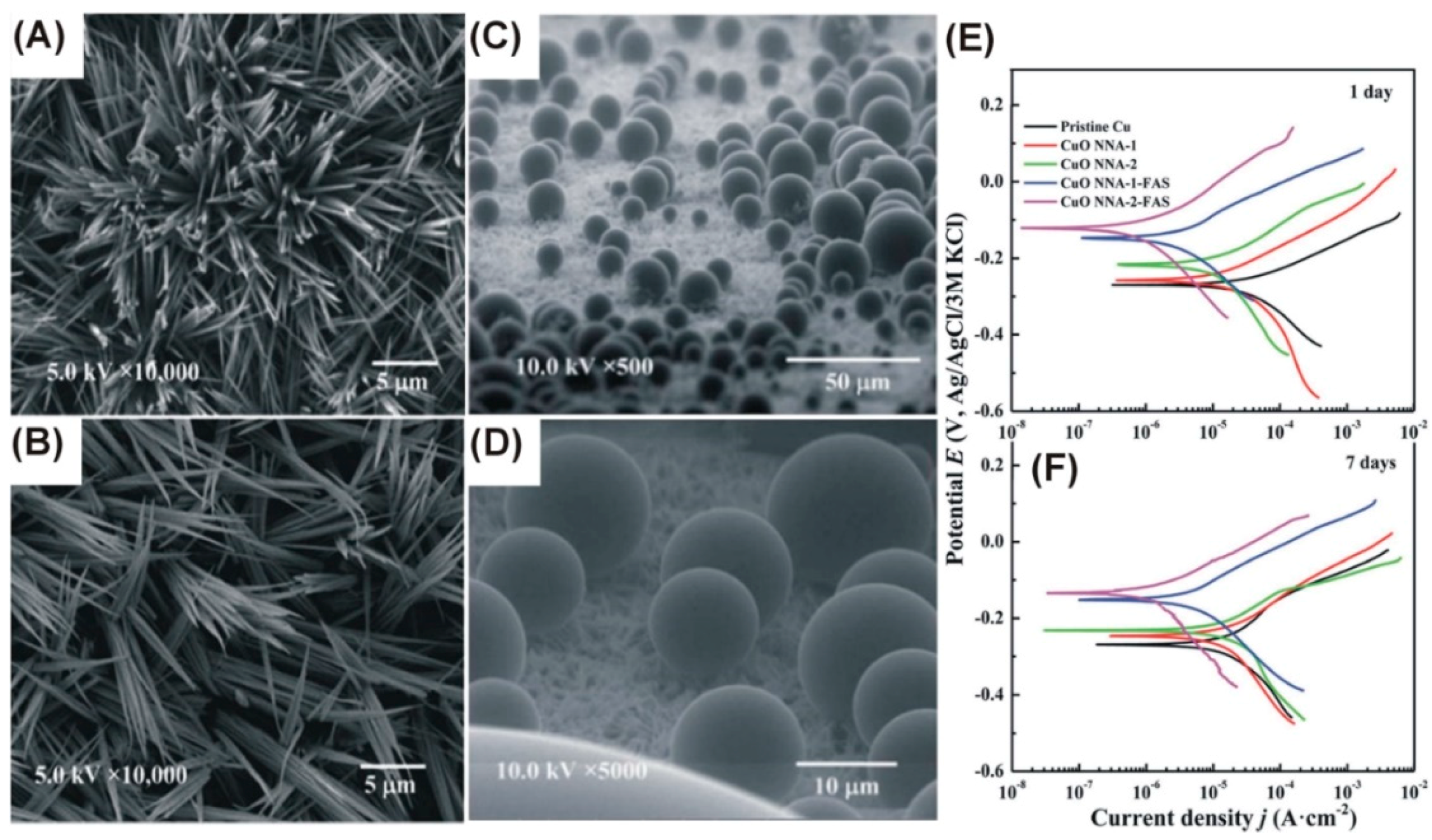
| 0.5–4.0 M KOH | 0.5–4.0 mA/cm2, 5–25 °C, 25 min | CuO nanoneedles 170 ± 40 nm in diameter 7–10 µm long | Fluoroalkyl-silane (FAS-17) was chemically bonded to CuO nanoneedles, increasing the contact angle up to 169° | Xiao 2015 [46] |
| 2, 2.5, 3, 3.5 M KOH | 1.5 mA/cm2, 2, 15, 28 °C | Cu(OH)2 and CuO nanoneedles 500–550 nm in diameter | Cu(OH)2 were turned into CuO nanoneedles using heat treatment (150 °C at 3 h + 200 °C at 3 h); in 3 M KOH at 28 °C nanotubes were formed (80–500 nm diameter, 10 µm length) | Wu 2005 [47] |
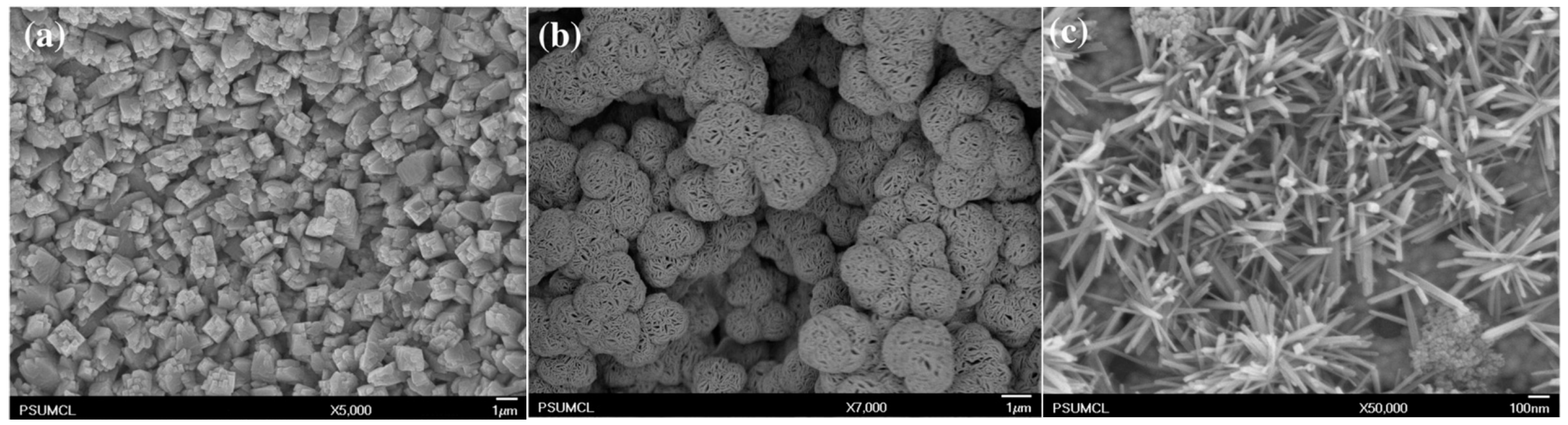
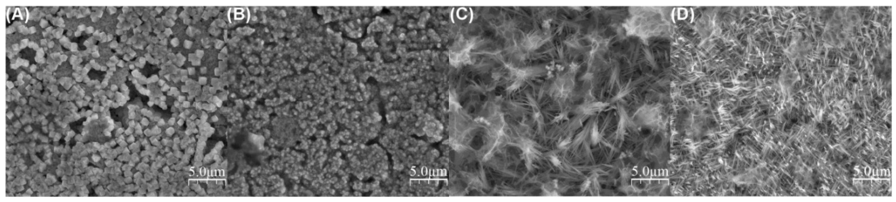
| 1 M KOH | −0.4, −0.3, −0.2, −0.1 V vs. Ag|AgCl, RT, 1 h | Morphology depends on the potential; cubes and nanowires | Formed nanowires were mixtures of Cu2O and CuO; nanowires were obtained for −0.2 (24 nm in diameter) and −0.1 V (19 nm in diameter), while for −0.4 and −0.3 V micro-cubes were formed | Stepniowski 2017 [41] |
| 0.15 M KOH + 0.1 M NH4Cl | 6 V, 300 s, RT | Cubes and dendrites | - | Allam 2011 [42] |
| 0.15 M KOH + 0.1 M NH4F | 6 V, 300 s, RT | Cu2O Micro-balls made of whiskers forming nanopores | 3 XPS and 4 GAXRD proved that the structures were made of Cu2O | Allam 2011 [42] |
| 0.15 M KOH + 0.1 M NH4F + 3% H2O in EG 2 | 30 V, 300 s, RT | 160-nm thick leaf-like architectures | When KOH concentration was increased to 0.2 M, the leaf-like structures were ca. 500 nm thick; at voltages below 30 V, no structured film was formed | Allam 2011 [42] |
| 0.75 wt % KOH + 3 wt % H2O + 0.20–0.35 wt % NaF in EG | 10–30 V, 10 min | Cu2O film | Cu2O film was formed by anodization; further annealing (250–450 °C, 60 min) allowed the growth of CuO nanowires, improving the photoelectrochemical performance | Wang 2013 [48] |
| 0.1–0.5 M KOH + 0–0.1 wt % NH4F + 1 vol % H2O in EG | 5–20 V, 5 °C | Nanoporous film (6–15 nm pore diameter) | Nanoporous oxide was formed, composed of a mixture of the following species: Cu2O, CuO, Cu(OH)2, and CuF2 | Oyarzún Jerez 2017 [49] |
| Chemical Composition of the Electrolyte | Experimental Conditions | Morphology and Chemical Composition of the Oxide | Remarks | Reference |
|---|---|---|---|---|
| 0.1 M NaOH | −400 mV, 1 h | Nanoparticles | Mechanism of oxide growth was studied | Caballero-Briones 2010 [51] |
| 0.1 M NaOH | 10 mV/s voltammetric scan from −1.2 to 0.8 V RT | Cu needle was anodized and coated by oxide-hydroxide film | Mechanism of Cu electrochemical oxidation was investigated | Wu 2013 [50] |
| 1 M NaOH | 0.06 mA/cm2, 5 min, 25 °C | Cu(OH)2 nanowires | Nanowires surface was modified by the chemical bonding of 1H,1H,2H,2H-Perfluorodecyltriethoxysilane (FAS-17) in order to increase the wetting contact angle to 154°; as-obtained nanowires were made of Cu(OH)2, but further annealing enabled the transofrmation of the hydroxide into CuO | Jiang 2015 [52] |
| 1 M NaOH | Cyclic voltammetry from −1.6 V to 0.4 V RT | CuO dendrite crystals grown on Cu2O nanoparticles | Cyclic voltammetric study of Cu in alkaline solution | Wan 2013 [53] |
| 3 M NaOH | 1.5, 3.0, 5.0 mA/cm2, 30 min | Cu2O, Cu2O/Cu(OH)2, Cu(OH)2 nanowires | Cu was electrodeposited on ITO (Indium Tin Oxide) and subsequently anodized; obtained nanostructures enhanced photocatalytic water splitting; the best results were achieved for nanowires made of both Cu2O and CuO | Zhang 2012 [54] |
| 0.15 M NaOH | pH = 12.8–13.0 −430 mV | Cu2O nanoparticles | Cu2O behaved like a p-type semiconductor | Caballero-Briones 2009 [55] |
| 1 M NaOH + 2.5 M NaCl + 0.5 g/L EG | 0.5–2.5 A/dm2, 55–70 °C, 30 min | 30-nm thick nanosheets made of CuO and Cu2O | Formed nanostructures are mixtures of CuO and Cu2O | Shu 2017 [56] |
| 10 wt % NaOH + 5 wt % NaClO2 | 0.75 V, 60 °C, 15 min | CuO films with traces of Cu3O2, decomposing to CuO and Cu2O | After anodizing, samples were immersed in KMnO4; consequently, solar light absorption reached up to 96% | Arurault 2007 [57] |
| 0.2 M NH4Cl; pH was adjusted to 8 with NaOH | 5 mA/cm2, RT, 20 min | Cu(OH)2 film | In order to transform Cu(OH)2 into Cu2O, three post-treatments were applied: hydrolysis in H2O2, reduction in H2 at 280 °C, redox with glucose; the H2O2 post-treated sample had the best efficiency in oxygen generation | Zhang 2015 [58] |
| Application | Role of the Anodically Grown Nanostructures | Remarks | Reference |
|---|---|---|---|
| Glucose sensor | High surface area Cu(III) active sites were reducted to Cu(II) by glucose | Glucose was determined at concentrations as low as 4 mM in human blood serum | [43] |
| pH-responsive water permeation mesh | High surface area | Wetting contact angle was pH-switchable and for a lower pH it reached up to 153° | [45] |
| High contact angle surface for corrosion protection | Highly-developed nanostructured surface area | Fluoroalkyl-silane (FAS-17) was chemically bonded to CuO nanoneedles, increasing the contact angle up to 169°; the corrosion performance was significantly improved | [46] |
| High contact angle surface | Highly-developed nanostructured surface area | Nanowires‘ surface was modified by the chemical bonding of 1H,1H,2H,2H-Perfluorodecyltriethoxysilane (FAS-17) in order to increase the wetting contact angle to 154° | [52] |
| Photoelectrochemical chemical water splitting | Highly-developed surface area and chemical composition (CuO-Cu2O) | Nanostructures enhanced photocatalytic water splitting; the best results were achieved for nanowires made of both Cu2O and CuO | [54] |
| Photochemical oxygen generation | High surface area and chemical composition (Cu2O) | Post-treatment of obtained nanostructures was conducted | [58] |
| Solar light absorption | Chemical composition (CuO with Cu3O2) | Post-treatment in KMnO4 was conducted | [57] |
| Fabrication Method | Drawbacks of the Method | Solution offered by Anodizing | Reference |
|---|---|---|---|
| Hydrothermal synthesis | Small aspect ratio of one-dimensioanl (1D) nanostructures; requires a few steps of synthesis | High aspect ratio of 1D nanostructures can be easily achieved by lengthening the time of anodization; facile, easy-to-scale-up two-step synthesis (electropolishing + anodizing) | [35,36] |
| Atomic layer deposition | Requires templates and expensive equipment to grow 1D nanostructures | Method based on easy to scale-up self-organization; inexpensive, electrochemical method | [35,36] |
| Solution-based chemical precipitation | Small aspect ratio of 1D nanostructures | Relatively high aspect ratio (see Table 1 and Table 2) | [35,36] |
| Template techniques (i.e., Anodic Aluminum Oxide, AAO and subsequent deposition) | Numerous steps of synthesis (formation of template, deposition, removal of the template) | An easy-to-conduct, two-step synthesis (electropolishing + anodizing) | [59] |
| Sol-gel techniques | Multistep process, time-consuming method | Anodization can be minutes long, in order to achieve a surface covered by oxide nanoneedles | [60] |
© 2018 by the authors. Licensee MDPI, Basel, Switzerland. This article is an open access article distributed under the terms and conditions of the Creative Commons Attribution (CC BY) license (http://creativecommons.org/licenses/by/4.0/).
Share and Cite
Stepniowski, W.J.; Misiolek, W.Z. Review of Fabrication Methods, Physical Properties, and Applications of Nanostructured Copper Oxides Formed via Electrochemical Oxidation. Nanomaterials 2018, 8, 379. https://doi.org/10.3390/nano8060379
Stepniowski WJ, Misiolek WZ. Review of Fabrication Methods, Physical Properties, and Applications of Nanostructured Copper Oxides Formed via Electrochemical Oxidation. Nanomaterials. 2018; 8(6):379. https://doi.org/10.3390/nano8060379
Chicago/Turabian StyleStepniowski, Wojciech J., and Wojciech Z. Misiolek. 2018. "Review of Fabrication Methods, Physical Properties, and Applications of Nanostructured Copper Oxides Formed via Electrochemical Oxidation" Nanomaterials 8, no. 6: 379. https://doi.org/10.3390/nano8060379
APA StyleStepniowski, W. J., & Misiolek, W. Z. (2018). Review of Fabrication Methods, Physical Properties, and Applications of Nanostructured Copper Oxides Formed via Electrochemical Oxidation. Nanomaterials, 8(6), 379. https://doi.org/10.3390/nano8060379