Wettability of Y2O3: A Relative Analysis of Thermally Oxidized, Reactively Sputtered and Template Assisted Nanostructured Coatings

Abstract
:1. Introduction


 . This model clearly demonstrates that the larger the vapor fraction (f2) the more hydrophobic is the surface.
2. Experimental Details
3. Results and Discussion
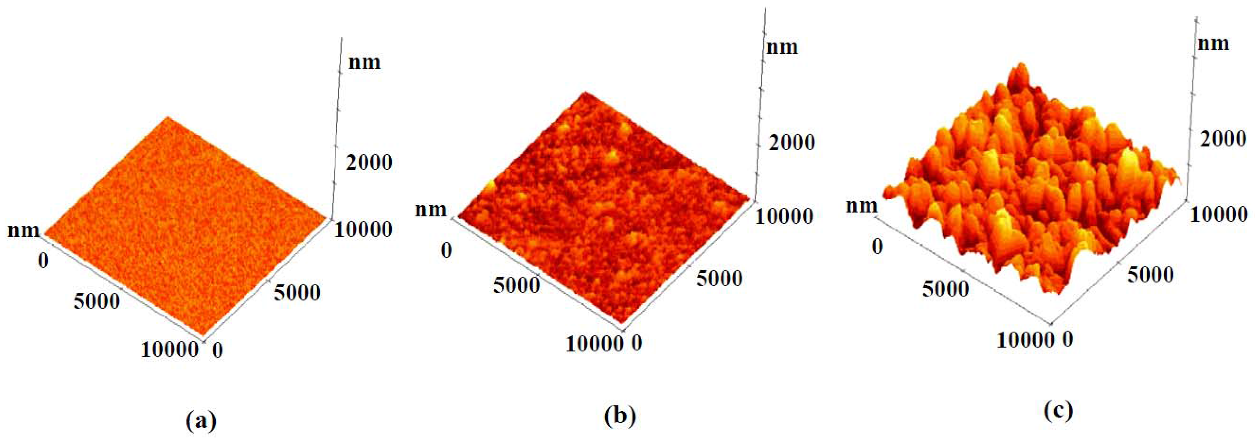
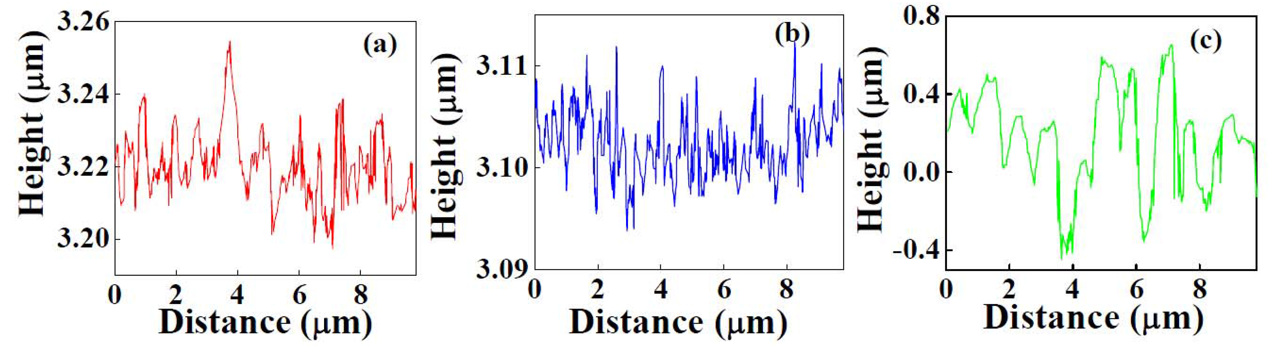
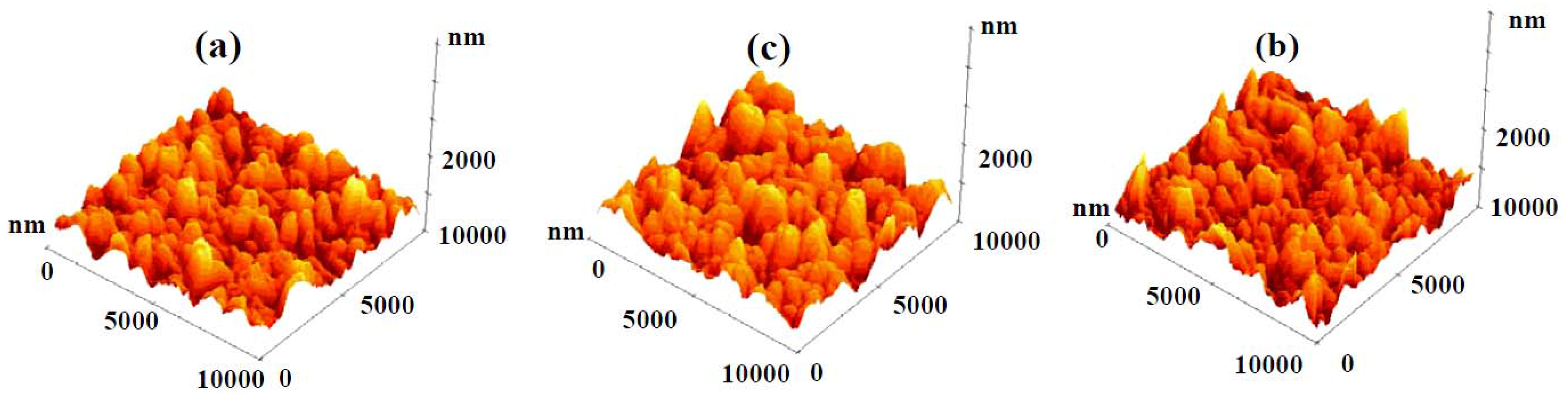
3.1. Structure and Morphology
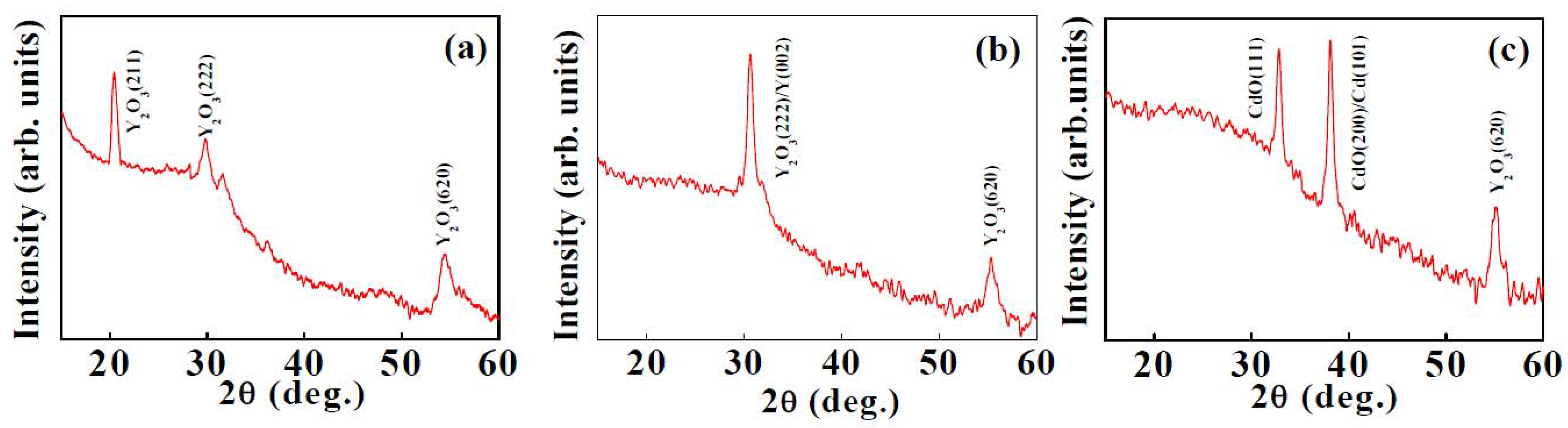
3.1.1. X-ray Diffraction

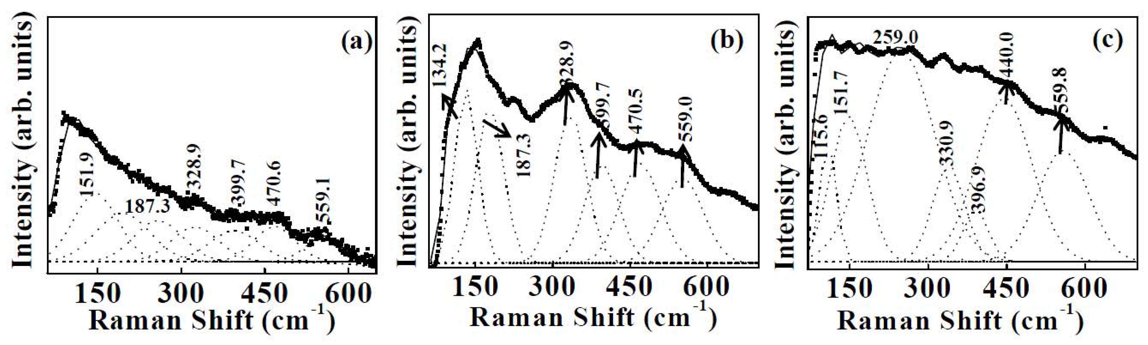
3.1.2. Micro-Raman Spectroscopy


| Sample 1 | Sample 2 | Sample 3 | |||
|---|---|---|---|---|---|
| Peak position (cm−1) | Symmetry | Peak position (cm−1) | Symmetry | Peak position (cm−1) | Symmetry |
| 151.9 | Fg+ Ag | 134.2 | Fg | 115.6 | Fg |
| 187.3 | Fg+ Eg | 187.3 | Fg+ Eg | 151.7 | Fg+ Ag |
| 328.9 | Fg+ Eg | 328.9 | Fg+ Eg | 330.9 | Fg+ Eg |
| 399.7 | Fg | 399.7 | Fg | 396.9 | Fg |
| 470.6 | Fg+ Ag | 470.5 | Fg+ Ag | 440.0 | Fg+ Eg |
| 559.1 | Fg+ Eg | 559.0 | Fg+ Eg | 559.8 | Fg+ Eg |
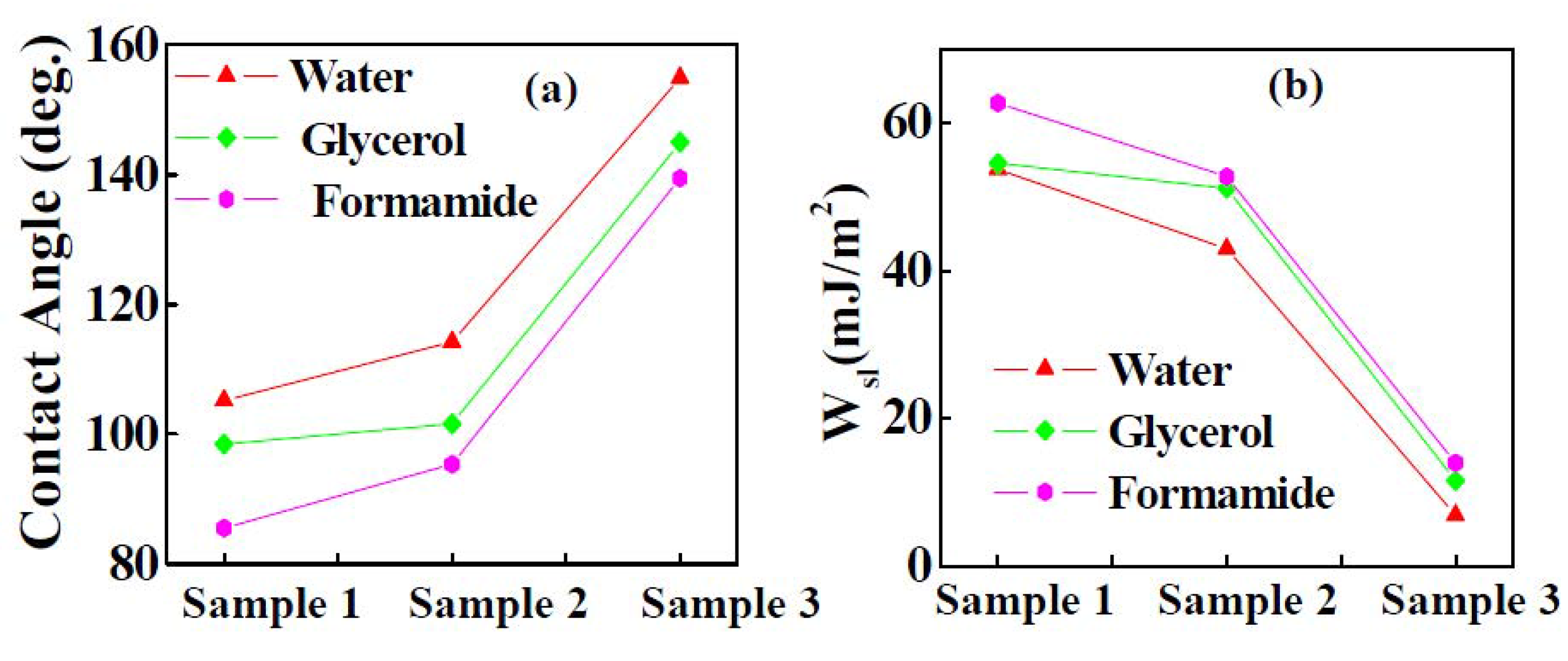
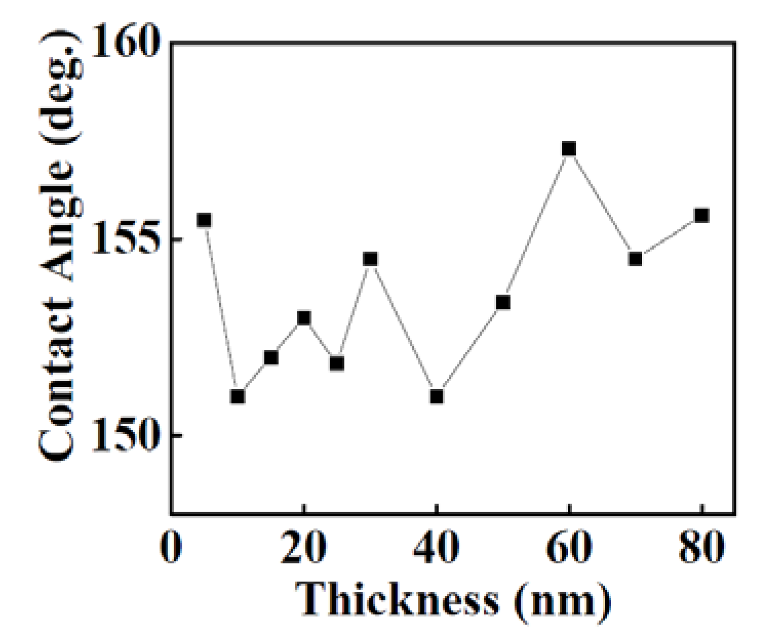
3.1.3. Wettability of Y2O3 Coatings
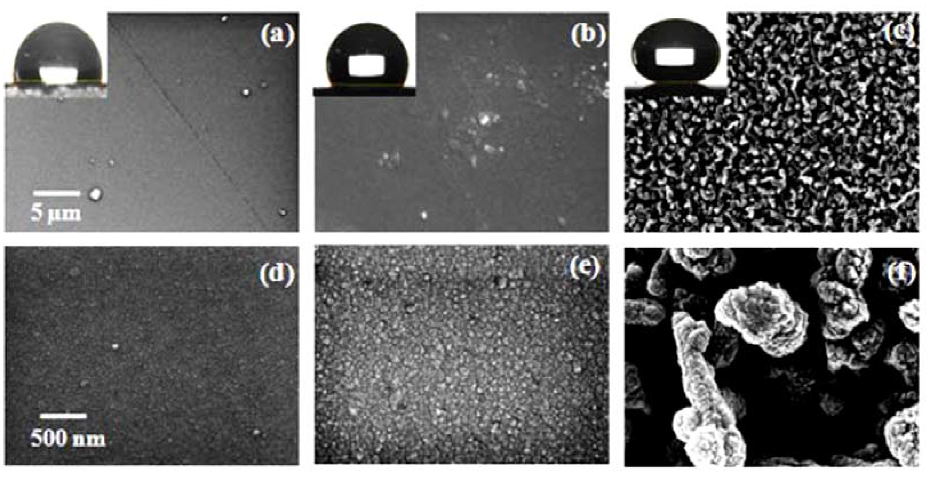


| Sample | Static contact angle (degree) | ||
|---|---|---|---|
| Water | Glycerol | Formamide | |
| Sample 1 | 99 | 98 | 85 |
| Sample 2 | 117 | 101 | 95 |
| Sample 3 | 155 | 145 | 139 |
4. Conclusions
Acknowledgements
References
- Wenzel, R.N. Resistance of solid surfaces to wetting by water. Ind. Eng. Chem. 1936, 28, 988–994. [Google Scholar] [CrossRef]
- Baxter, S.; Cassie, A.B.D. Wettability of porous surfaces. Trans. Faraday Soc. 1944, 40, 546–551. [Google Scholar] [CrossRef]
- Chatelain, F.; Delapierre, G.; Obeid, P.; Pegon, P.; Getin, S.; Brachet, A.G.; Fouque, B. Improvement of yeast biochip sensitivity using multilayer inorganic sol-gel substrates. Biosens. Bioelectron. 2007, 22, 2151–2157. [Google Scholar] [CrossRef] [PubMed]
- Galvin, P.; Wood, T.; Rawely, O.; Moore, E. Monitoring of cell growth in vitro using biochips packaged with indium tin oxide sensors. Sens. Actuator. B Chem. 2009, 139, 187–193. [Google Scholar] [CrossRef]
- Ohab, M.; Gotou, T.; Hirata, M. Thin-film particles of graphite oxide. 2: Preliminary studies for internal micro fabrication of single particle and carbonaceous electronic circuits. Carbon 2005, 43, 503–510. [Google Scholar] [CrossRef]
- Wang, M.; Han, S.; Peng, R.; Guo, Y.; Geng, H. A facile route for preparation of conjugated polymer functionalized inorganic semiconductors and direct application in hybrid photovoltaic devices. Solar Energy Mater. Solar Cells 2010, 94, 1293–1299. [Google Scholar] [CrossRef]
- Passacantando, M.; Santucci, S.; Cantalini, C.; Sberveglieri, G.; Comini, E.; Wlodarski, W.; Li, Y.X.; Galatsis, K. Comparison of single and binary oxide MoO3, TiO2 and WO3 sol-gel sensors. Sens. Actuator. B Chem. 2002, 83, 276–280. [Google Scholar] [CrossRef]
- Lamdhade, G.T.; Yawale, S.S.; Yawale, S.P. Tin oxide and zinc oxide based doped humidity sensors. Sens. Actuator. A 2007, 135, 388–393. [Google Scholar] [CrossRef]
- Li, H.D.; Sun, X.D.; Wu, X.H.; Ma, C.L.; Wang, Y.D. Electrical and gas-sensing properties of mesostructured tin oxide-based H2 sensors. Sens. Actuator. B Chem. 2002, 85, 270–276. [Google Scholar] [CrossRef]
- Akins, D.L.; Stevens, N. Dye-doped inorganic/organic composite films as fluorescence sensors for methanol vapor. Sens. Actuator. B Chem. 2007, 123, 59–64. [Google Scholar] [CrossRef]
- Basu, S.; Saha, H.; Basu, P.K.; Bhattacharyya, P. Fast response methane sensor using nanocrystalline zinc oxide thin films derived by sol–gel method. Sen. Actuator. B Chem. 2007, 124, 62–67. [Google Scholar] [CrossRef]
- Yi, J.; Kwak, D.J.; Lim, D.G. Improved interface properties of yttrium oxide buffer layer on silicon substrate for ferroelectric random access memory applications. Thin Solid Films 2002, 422, 150–154. [Google Scholar] [CrossRef]
- Shiratori, S.; Fujimoto, K.; Kim, J.; Ogawa, T.; Ding, B. Fabrication of a superhydrophobic nanofibrous zinc oxide film surface by electro-spinning. Thin Solid Films 2008, 516, 2495–2501. [Google Scholar] [CrossRef]
- Yan, H.; Song, X.; Zhang, X. H.; Li, E.; Wang, B.; Pei, M. D. The fabrication of superhydrophobic copper films by a low-pressure-oxidation method. Appl. Surf. Sci. 2010, 256, 5824–5827. [Google Scholar] [CrossRef]
- Liu, W.; Hao, J.; Zhou, F.; Guo, Z. Stable biomimetic superhydrophobic engineering materials. J. Am. Chem. Soc. 2005, 127, 15670–15671. [Google Scholar] [CrossRef] [PubMed]
- Gogolides, E.; Tserepi, A.; Papageorgiou, D.; Tsougeni, K. “Smart” polymeric microfluidics fabricated by plasma processing: Controlled wetting, capillary filling and hydrophobic valving. Lab Chip 2010, 10, 462–469. [Google Scholar] [CrossRef] [PubMed]
- Jiang, L.; Zhai, J.; Feng, X. The fabrication and switchable superhydrophobicity of TiO2 nanorod films. Angew. Chem. Int. Ed. 2005, 44, 5115–5118. [Google Scholar] [CrossRef]
- Nistchke, M.; Motornov, M.; Muller, M.; Minko, S. Two-level structured self-adaptive surfaces with reversibly tunable properties. J. Am. Chem. Soc. 2003, 125, 3896–3900. [Google Scholar] [CrossRef] [PubMed]
- Jiang, L.; Gao, X.; Feng, L.; Sun, T. Bio-inspired surfaces with special wettability. Acc. Chem. Res. 2005, 38, 644–652. [Google Scholar] [CrossRef] [PubMed]
- Jiang, L.; Yao, J.; Feng, X.; Wang, S. Controlling wettability and photochromism in a dual-responsive tungsten oxide film. Angew. Chem. Int. Ed. 2006, 45, 1264–1267. [Google Scholar] [CrossRef]
- Lkkala, O.; Ras, R.H.A.; Ritala, M.; Lindstrom, T.; Ankerfors, M.; Kemell, M.; Pore, V.; Sainio, J.; Ruokolainen, J.; Nykanen, A.; Houbenov, N.; Silvennoinen, R.J.; Kettunen, M. Photoswitchable superabsorbency based on nanocellulose aerogels. Adv. Funct. Mater. 2011, 21, 510–517. [Google Scholar] [CrossRef]
- Ras, R.H.; Karppinen, M.; Sahramo, E.; Malm, J. A photo-controlled wettability switching by conformal coating of nanoscale topographies with ultrathin oxide films. Chem. Mater. 2010, 22, 3349–3352. [Google Scholar] [CrossRef]
- Popov, D.; Thielsch, R.; Atanassov, G. Optical properties of TiO2, Y2O3, and CeO2 thin films deposited by electron beam evaporation. Thin Solid Films 1993, 223, 288–292. [Google Scholar] [CrossRef]
- Perriere, J.; Pailloux, F.; Gaboriaud, R.J. Pulsed laser deposition of Y2O3 thin film on MgO. Appl. Surf. Sci. 2002, 186, 477–482. [Google Scholar] [CrossRef]
- Kennedy, I.M.; Guo, B.; Dosev, D. Photoluminescence of Eu3 + : Y2O3 as an indication of crystal structure and particle size in nanoparticles synthesized by flame spray pyrolysis. J. Aerosol Sci. 2006, 37, 402–412. [Google Scholar] [CrossRef]
- Garcia, M.; Guasti, M.F.; Diamant, R.; Poniatowski, E.H.; Alonso, J.C. Photoluminescent thin films of terbium chloride-doped yttrium oxide deposited by the pulsed laser ablation technique. Thin Solid Films 1997, 303, 76–83. [Google Scholar] [CrossRef]
- Bose, A.C.; Joseyphus, R.J.; Elanchezhiyan, J.; Yogamalar, N.R.; Srinivasan, R. Structural and optical properties of europium doped yttrium oxide nanoparticles for phosphor applications. J. Alloys Compd. 2010, 496, 472–477. [Google Scholar] [CrossRef]
- Srikumar, S.R.; Mahalingam, T.; Auluck, S. Controlled synthesis, optical and electronic properties of Eu3+ doped yttrium oxysulfide (Y2O2S) nanostructures. J. Colloid Interface Sci. 2009, 336, 889–897. [Google Scholar] [CrossRef] [PubMed]
- Mugnier, J.; Garapon, C.; Perriere, J.; Millon, E.; Viana, B.; Aschehoug, P.; Fidancev, E.A.; Huignard, A.; Moll, O.P.Y. Eu3+and Tm3+ doped yttrium oxide thin films for optical applications. J. Luminesc 2000, 87–89. [Google Scholar]
- Fu, L.; Tanner, P.A. Morphology of Y2O3: Eu3+ prepared by hydrothermal synthesis. Chem. Phys. Lett. 2009, 470, 75–79. [Google Scholar] [CrossRef]
- Muroga, T.; Terai, T.; Koch, F.; Maier, H.; Suzuki, A.; Sawada, A. Fabrication of yttrium oxide and erbium oxide coatings by PVD methods. Fusion Eng. Des. 2005, 75, 737–740. [Google Scholar] [CrossRef]
- Xianping, F.; Pengyue, Z.; Shizhu, Z.; Zhanglian, H.; Huang, G. Synthesis of yttrium oxide nanocrystal via solvothermal process. J. Rare Earths 2006, 24, 47–50. [Google Scholar] [CrossRef]
- Tudoran, L.B.; Grecu, R.; Popovici, E.J.; Muresan, L. Studies on the synthesis of europium activated yttrium oxide by wet-chemical method: 1. Influence of precursor quality on phosphor photoluminescence properties. J. Alloys Compd. 2009, 471, 421–427. [Google Scholar] [CrossRef]
- Paumier, F.; Guerin, P.; Pailloux, F.; Gaboriaud, R.J. Yttrium oxide thin films, Y2O3, grown by ion beam sputtering on Si. J. Phys. D Appl. Phys. 2000, 33, 2884–2889. [Google Scholar] [CrossRef]
- Shih, I.; Yip, L.S. Studies of yttrium oxide films prepared by magnetron sputtering. Electron. Lett. 1988, 24, 1287–1288. [Google Scholar] [CrossRef]
- Dai, B.; Lei, P.; Tian, G.; Han, J.; Weng, Y.; Shen, W.; Zhu, Y.; Zhu, J. Growth and characterization of yttrium oxide films by reactive magnetron sputtering. Thin Solid Films 2011, 519, 4894–4898. [Google Scholar] [CrossRef]
- Qian, Y.; Liu, X.; Zhang, S.; Li, S.; Liu, Z.; Tang, Q. Synthesis of yttrium hydroxide and nanotubes. J. Cryst. Growth 2003, 259, 208–214. [Google Scholar] [CrossRef]
- Pengyue, Z.; Lixia, P.; Qichao, Z.; Zhanglian, H.; Zhenxiu, X. Preparation and luminescence properties of Y2O3: Eu3+ nanorods via post annealing process. J. Rare Earths 2006, 24, 111–114. [Google Scholar] [CrossRef]
- Rajam, K.S.; Barshilia, H.C. Sputter deposited nanometric multi-scale rough Cd-CdO superhydrophobic thin films. Nanosci. Nanotechnol. Lett. 2011, 3, 300–305. [Google Scholar] [CrossRef]
- Beny, J.M.; Husson, E.; Proust, C.; Repelin, Y. Vibrational spectroscopy of the C-form of yttrium sesquioxide. J. Solid State Chem. 1995, 118, 163–169. [Google Scholar] [CrossRef]
- Yoshimura, M.; Kakihana, M.; Lee, J.H.; Yashima, M. Raman spectral characterization of existing phase in the Y2O3-Nb2O5 system. J. Phys. Chem. Solids 1997, 58, 1593–1597. [Google Scholar] [CrossRef]
- Yalamanchili, M.R.; Drelich, J.; Veeramasuneni, S.; Miller, J.D. Effect of roughness determined by atomic force microscopy on the wetting properties of PTFE thin films. Polym. Eng. Sci. 1996, 36, 1849–1855. [Google Scholar] [CrossRef]
- Rajam, K.S.; Devi, L.M.; Pillai, N.; Selvakumar, N.; Barshilia, H.C. Wettability of ZnO: A comparison of reactively sputtered; thermally oxidized and vacuum annealed coating. Appl. Surf. Sci. 2011, 257, 4410–4417. [Google Scholar] [CrossRef]
- Rajam, K.S.; Barshilia, H.C.; Selvakumar, N. Effect of substrate roughness on the surface free energy of sputter deposited superhydrophobic polytetrafluoroethylene coatings: A comparison of experimental data with different theoretical models. J. Appl. Phys. 2010, 108, 013505:1–013505:9. [Google Scholar]
- Cazin, A.A.; Arnthal, M.; Zeuner, G. Theorie Mechanique De La Chaleur, Avec Ses Applications Aux Machines; 1869; pp. 1828–1907. Gauthier-Villars: Paris, France. [Google Scholar]
© 2012 by the authors. This article is an open-access article distributed under the terms and conditions of the Creative Commons Attribution license ( http://creativecommons.org/licenses/by/3.0/).
Share and Cite
Barshilia, H.C.; Chaudhary, A.; Kumar, P.; Manikandanath, N.T. Wettability of Y2O3: A Relative Analysis of Thermally Oxidized, Reactively Sputtered and Template Assisted Nanostructured Coatings. Nanomaterials 2012, 2, 65-78. https://doi.org/10.3390/nano2010065
Barshilia HC, Chaudhary A, Kumar P, Manikandanath NT. Wettability of Y2O3: A Relative Analysis of Thermally Oxidized, Reactively Sputtered and Template Assisted Nanostructured Coatings. Nanomaterials. 2012; 2(1):65-78. https://doi.org/10.3390/nano2010065
Chicago/Turabian StyleBarshilia, Harish C., Archana Chaudhary, Praveen Kumar, and Natarajan T. Manikandanath. 2012. "Wettability of Y2O3: A Relative Analysis of Thermally Oxidized, Reactively Sputtered and Template Assisted Nanostructured Coatings" Nanomaterials 2, no. 1: 65-78. https://doi.org/10.3390/nano2010065