Process Oxygen Flow Influence on the Structural Properties of Thin Films Obtained by Co-Sputtering of (TeO2)x-ZnO and Au onto Si Substrates


Abstract
:
1. Introduction
2. Materials and Methods
3. Results and Discussion
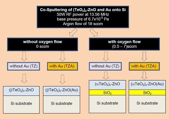
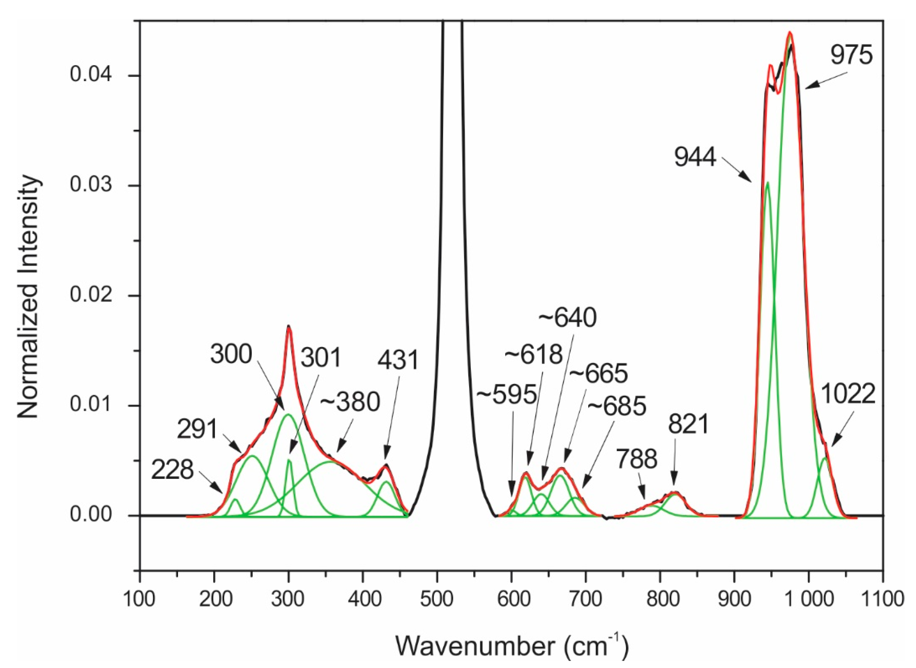
3.1. Structural Properties of TZ/Si
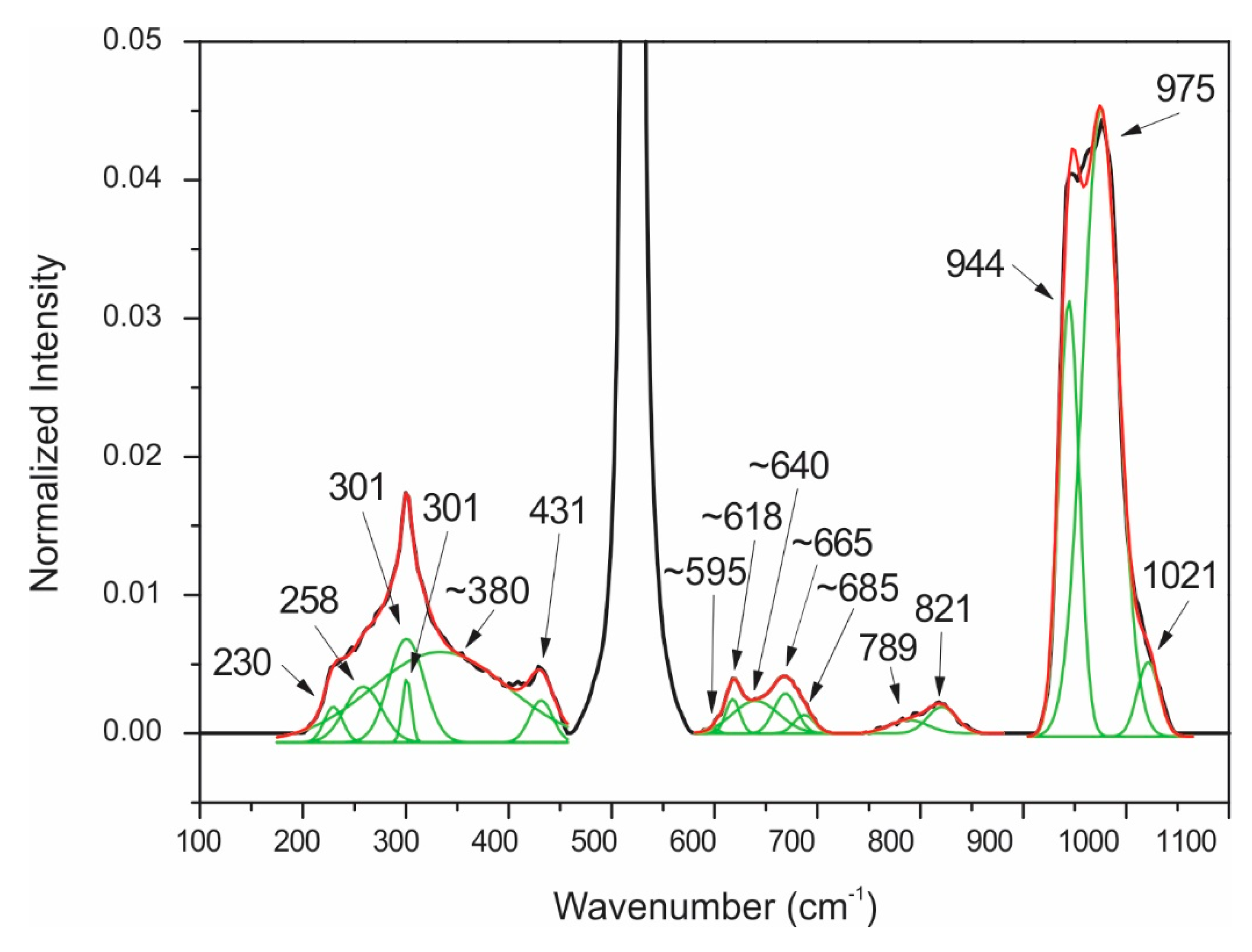
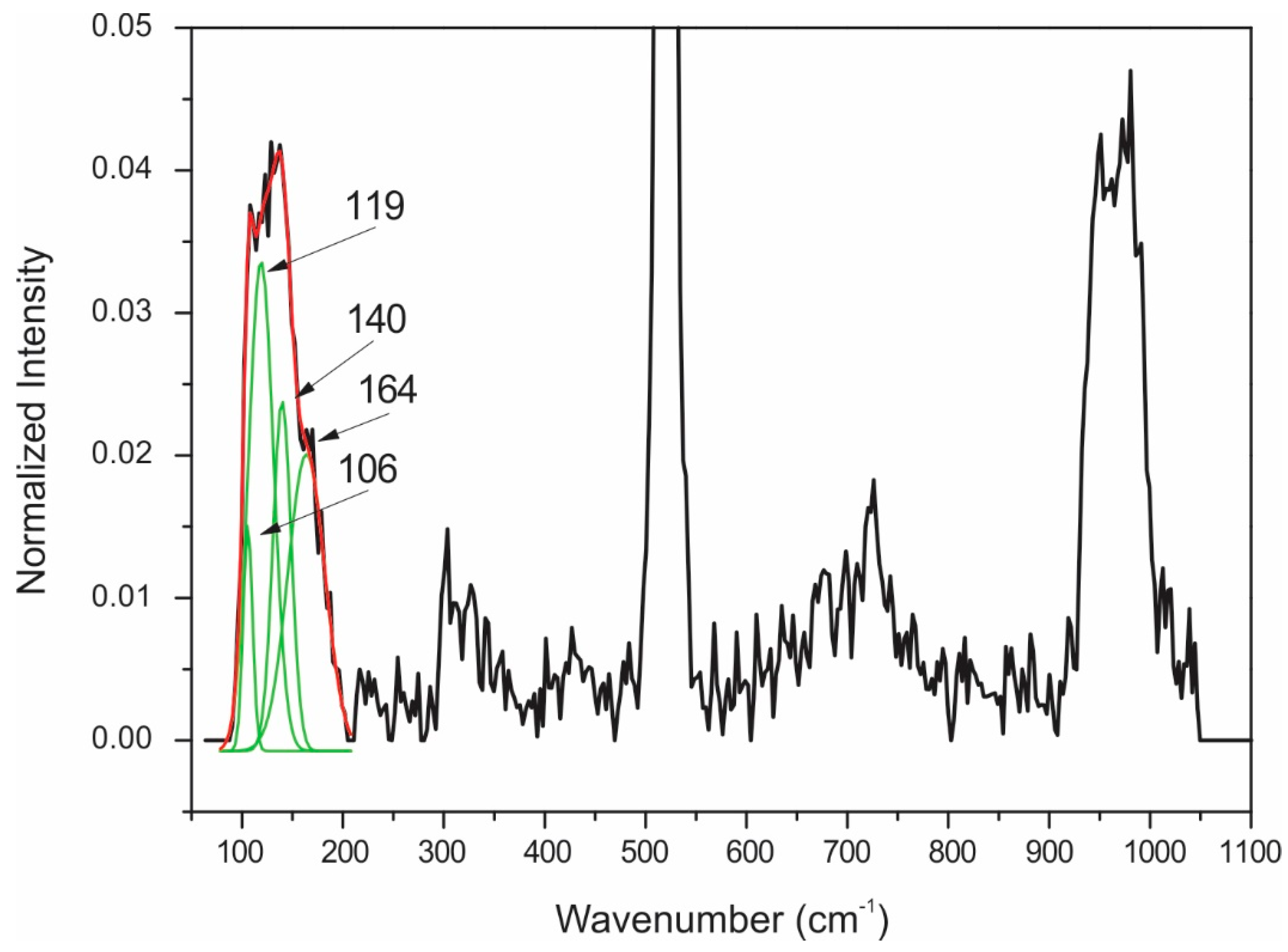
3.2. Structural Properties of TZA/Si
4. Conclusions
Author Contributions
Funding
Acknowledgments
Conflicts of Interest
Appendix A

References
- De Assumpção, T.A.; Da Silva, D.M.; Camilo, M.E.; Kassab, L.R.P.; Gomes, A.S.L.; De Araujo, C.B.; Wetter, N.U.; De Assumpção, T.A.A. Frequency upconversion properties of Tm3+ doped TeO2–ZnO glasses containing silver nanoparticles. J. Alloy. Compd. 2012, 536, S504–S506. [Google Scholar] [CrossRef]
- Kassab, L.R.P.; Freitas, L.F.; De Assumpção, T.A.A.; Da Silva, D.M.; De Araujo, C.B.; Da Silva, D.M. Frequency upconversion properties of Ag: TeO2–ZnO nanocomposites codoped with Yb3+ and Tm3+ ions. Appl. Phys. A 2011, 104, 1029–1034. [Google Scholar] [CrossRef]
- Da Silva, D.S.; De Assumpção, T.A.A.; De Simone, G.B.C.; Kassab, L.R.P.; De Araujo, C.B. Enhanced Er3+ photoluminescence in TeO2–ZnO glass containing silicon nanocrystals. Appl. Phys. A 2015, 121, 117–121. [Google Scholar] [CrossRef]
- Moreira, L.; Falci, R.; Darabian, L.M.; Anjos, V.; Bell, M.; Kassab, L.R.P.; Bordon, C.; Doualan, J.-L.; Camy, P.; Moncorgé, R. The effect of excitation intensity variation and silver nanoparticle codoping on nonlinear optical properties of mixed tellurite and zinc oxide glass doped with Nd2O3 studied through ultrafast z-scan spectroscopy. Opt. Mater. 2018, 79, 397–402. [Google Scholar] [CrossRef] [Green Version]
- Moreira, L.; Anjos, V.; Bell, M.J.V.; Ramos, C.; Kassab, L.R.P.; Doualan, D.; Camy, P.; Moncorge, R. The effects of Nd2O3 concentration in the laser emission of TeO2-ZnO glasses. Opt. Mater. 2016, 58, 84–88. [Google Scholar] [CrossRef] [Green Version]
- Bell, M.J.V.; Anjos, V.; Moreira, L.M.; Falci, R.F.; Kassab, L.R.P.; Da Silva, D.S.; Doualan, J.-L.; Camy, P.; Moncorgé, R. Laser emission of a Nd-doped mixed tellurite and zinc oxide glass. J. Opt. Soc. Am. B 2014, 31, 1590. [Google Scholar] [CrossRef] [Green Version]
- Florêncio, L.D.A.; Gómez-Malagón, L.A.; Lima, B.C.; Gomes, A.S.L.; Garcia, J.; Kassab, L.R.P. Efficiency enhancement in solar cells using photon down-conversion in Tb/Yb-doped tellurite glass. Sol. Energy Mater. Sol. Cells 2016, 157, 468–475. [Google Scholar] [CrossRef] [Green Version]
- Lima, B.C.; Gómez-Malagón, L.A.; Gomes, A.S.L.; Garcia, J.A.M.; Kassab, L. Plasmon-Assisted Efficiency Enhancement of Eu3+-Doped Tellurite Glass-Covered Solar Cells. J. Electron. Mater. 2017, 46, 6750–6755. [Google Scholar] [CrossRef]
- El-Mallawany, R. Ultrasonic Detection of Microphase Separation in Tellurite Glasses. Phys. Status Solidi 1992, 133, 245–251. [Google Scholar] [CrossRef]
- Kozhukharov, V.; Bürger, H.; Neov, S.; Sidzhimov, B. Atomic arrangement of a zinc-tellurite glass. Polyhedron 1986, 5, 771–777. [Google Scholar] [CrossRef]
- Mirgorodsky, A.; Merle-Mejean, T.; Champarnaud, J.-C.; Thomas, P.; Frit, B. Dynamics and structure of TeO2 polymorphs: model treatment of paratellurite and tellurite; Raman scattering evidence for new γ- and δ-phases. J. Phys. Chem. Solids 2000, 61, 501–509. [Google Scholar] [CrossRef]
- Bontempo, L.; Filho, S.D.S.; Kassab, L. Conduction and reversible memory phenomena in Au-nanoparticles-incorporated TeO2–ZnO films. Thin Solid Films 2016, 611, 21–26. [Google Scholar] [CrossRef]
- Beyer, H. Verfeinerung der Kristallstruktur von Tellurit, dem rhombischen TeO2. Z. Für Krist. Cryst. Mater. 1967, 124, 228–237. [Google Scholar] [CrossRef]
- Greenwood, N.; Earnshaw, A. Chemistry of the Elements; Elsevier: Amsterdam, The Netherlands, 1984; p. 911. [Google Scholar]
- Kondratyuk, I.P.; Muradyan, L.A.; Pisarevsky, I.V.; Simonov, V.I. Precision X-ray structural investigation of acousto-optical single crystals of α-TeO2. Kristallografiya 1987, 32, 609. [Google Scholar]
- Thomas, P.A. The crystal structure and absolute optical chirality of paratellurite, α-TeO2. J. Phys. C Solid State Phys. 1988, 21, 4611–4627. [Google Scholar] [CrossRef]
- McWhinnie, W.R. Tellurium—Inorganic chemistry. In Encyclopedia of Inorganic Chemistry; King, B., Ed.; Wiley: New York, NY, USA, 1994. [Google Scholar]
- Chagraoui, A.; Yakine, I.; Tairi, A.; Moussaoui, A.; Talbi, M.; Naji, M. Glasses formation, characterization, and crystal-structure determination in the Bi2O3–Sb2O3–TeO2 system prepared in an air. J. Mater. Sci. 2011, 46, 5439–5446. [Google Scholar] [CrossRef] [Green Version]
- Roberts, A.C.; Grice, J.D.; Groat, L.A.; Criddle, A.J.; Gault, R.A.; Erd, R.C.; Moffatt, E.A. Jensenitte, Cu3Te6 +O6.2H2O, a new mineral species from the Centennial Eureka Mine, Tintic District, Juab County, Utah. Can. Mineral. 1996, 34, 49–54. [Google Scholar]
- Roberts, A.C.; Groat, L.A.; Grice, J.D.; Gault, R.A.; Jensen, M.C.; Moffatt, E.A.; Stirling, J.A.R. Leisingite, Cu(Mg,Cu,Fe,Zn)2Te6+O6·6H2O, a new mineral species from the Centennial Eureka mine, Juab County, Utah. Miner. Mag. 1996, 60, 653–657. [Google Scholar] [CrossRef]
- Christy, A.G.; Mills, S.J.; Kampf, A.R. A review of the structural architecture of tellurium oxycompounds. Miner. Mag. 2016, 80, 415–545. [Google Scholar] [CrossRef] [Green Version]
- Frost, R.L.; Keeffe, E.C. Raman spectroscopic study of kuranakhite PbMn4+ Te6+ O6 -a rare tellurate mineral. J. Raman Spectrosc. 2008, 40, 249–252. [Google Scholar] [CrossRef] [Green Version]
- Kern, W.; Puotinen, D.A. Cleaning Solution Based on Hydrogen Peroxide for use in Silicon Semiconductor Technology. RCA Rev. 1970, 31, 187–206. [Google Scholar]
- File, P.D. JCPDS International Centre for Diffraction Data; ICDD: Newtown Square, PA, USA, 1998. [Google Scholar]
- Mayer, M. SIMNRA, a simulation program for the analysis of NRA, RBS and ERDA. AIP Conf. Proc. 1999, 475, 541–544. [Google Scholar]
- Rodrigues, A.; Keding, R.; Rüssel, C. Mixed former effect between TeO2 and SiO2 in the Li2O·TeO2·SiO2 system. J. Non Cryst. Solids 2000, 273, 53–58. [Google Scholar] [CrossRef]
- Pine, A.S.; Dresselhaus, G. Raman Scattering in Paratellurite, TeO2. Phys. Rev. B 1972, 5, 4087–4093. [Google Scholar] [CrossRef]
- Yadav, A.K.; Singh, P. A review of the structures of oxide glasses by Raman spectroscopy. RSC Adv. 2015, 5, 67583–67609. [Google Scholar] [CrossRef]
- Siebert, H. Ultrarotspektren von Tellursäuren, Telluraten und Antimonaten. Z. Für Anorg. Allg. Chem. 1959, 301, 161–170. [Google Scholar] [CrossRef]
- Paweł; Paweł; Borowicz; Latek, M.; Rzodkiewicz, W.; Łaszcz, A.; Czerwinski, A.; Ratajczak, J. Deep-ultraviolet Raman investigation of silicon oxide: thin film on silicon substrate versus bulk material. Adv. Nat. Sci. Nanosci. Nanotechnol. 2012, 3, 45003. [Google Scholar] [CrossRef]
- Li, Q.; Gu, M.; Du, Y.; Xian, X. TeO2 -SiO2/α -TeO2 Composite Film Prepared by Electrochemical sol-gel Method and Its Non-linear Optical Properties. Acta Chim. Sin. 2012, 70, 572. [Google Scholar] [CrossRef] [Green Version]
- Li, Q.; Gu, M. Preparation of TeOx–SiO2 film with excellent third-order nonlinear optical properties by electrochemically induced sol–gel method. Chin. Chem. Lett. 2011, 22, 1359–1362. [Google Scholar] [CrossRef]
- Deal, B.E.; Grove, A.S. General Relationship for the Thermal Oxidation of Silicon. J. Appl. Phys. 1965, 36, 3770. [Google Scholar] [CrossRef] [Green Version]
- Filho, S.G.D.S.; Hasenack, C.M.; Lopes, M.C.V.; Baranauskas, V. Rapid thermal oxidation of silicon with different thermal annealing cycles in nitrogen: Influence on surface microroughness and electrical characteristics. Semicond. Sci. Technol. 1995, 10, 990–996. [Google Scholar] [CrossRef]
- Filho, S.G.D.S.; Hasenack, C.M.; Salay, L.C.; Mertens, P. A Less Critical Cleaning Procedure for Silicon Wafer Using Diluted HF Dip and Boiling in Isopropyl Alcohol as Final Steps. J. Electrochem. Soc. 2019, 142, 902–907. [Google Scholar] [CrossRef]
- Jiang, H.-L.; Mao, J.-G. Synthesis, Crystal Structure and Characterization of the Barium Zinc Tellurate Disilicate: Ba3Zn6[TeO6][Si2O7]2. Z. Für Anorg. Allg. Chem. 2006, 632, 2053–2057. [Google Scholar] [CrossRef]
- Jiang, H.-L.; Mao, J.-G. Synthesis, Crystal Structure and Characterization of the Barium Zinc Tellurate Disilicate: Ba3Zn6[TeO6] [Si2O7]2. ChemInform 2006, 632, 2053–2057. [Google Scholar] [CrossRef]
- Van Loosdrecht, P.H.M.; Van Bentum, P.J.M.; Balzuweit, K. Raman study of incommensurately modulated calaverite (AuTe 2). Ferroelectrics 1992, 125, 517–522. [Google Scholar] [CrossRef]
- Hong, S.; Li, X. Optimal Size of Gold Nanoparticles for Surface-Enhanced Raman Spectroscopy under Different Conditions. J. Nanomater. 2013, 2013, 790323. [Google Scholar] [CrossRef]
- Feutelais, Y.; Mouani, D.; Didry, J.R.; Legendre, B. The gold-tellurium system. J. Phase Equilibria Diffus. 1994, 15, 380–385. [Google Scholar] [CrossRef]


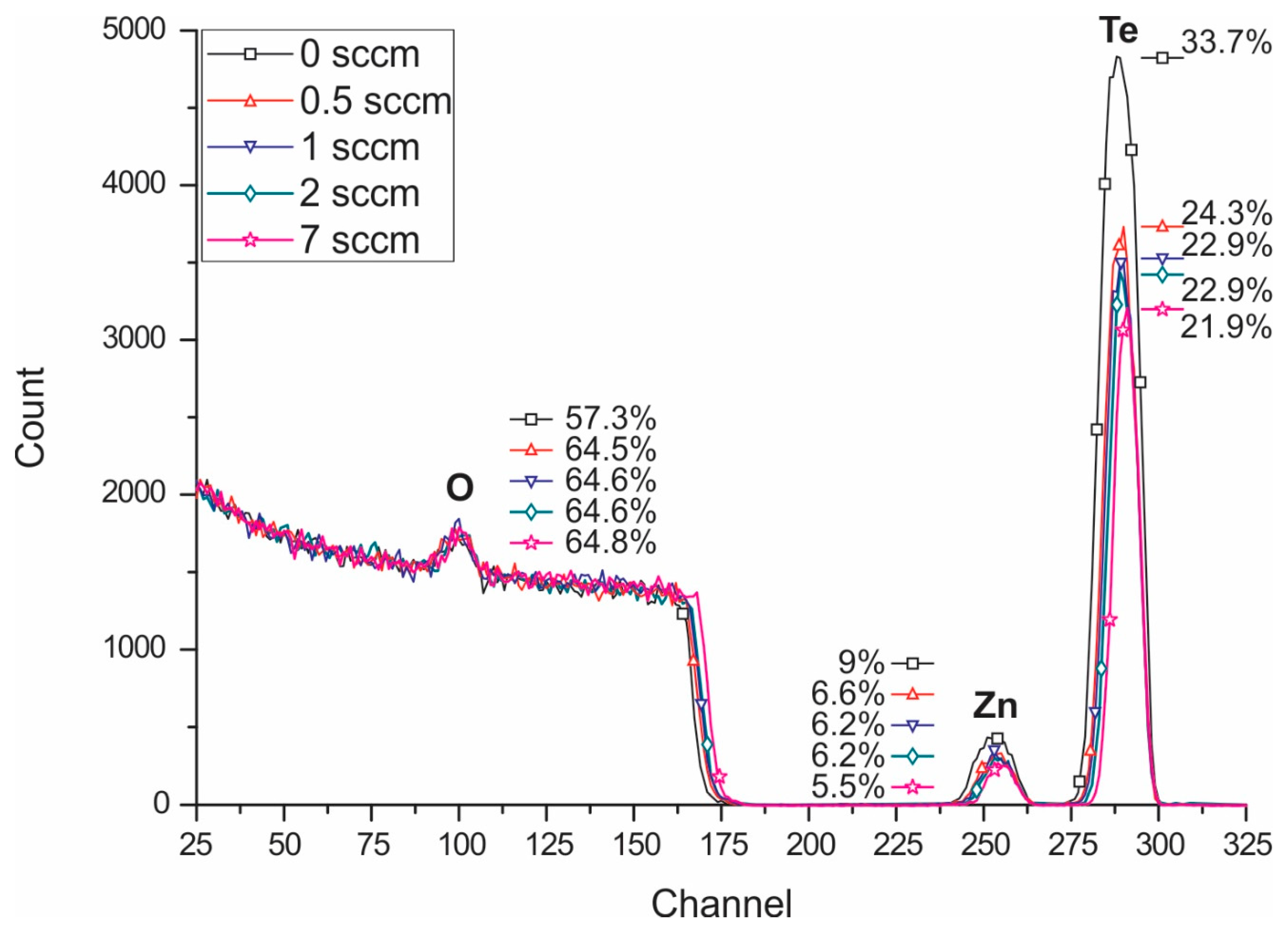
| 0 sccm 1 0 h | 0 sccm 10 h | ||
| 101 | β 2 | 101 | β |
| 125 | β | 122 | β |
| 136 | β | ||
| 140 | β | 140 | β |
| 222 | β | 223 | β |
| 268 | β | 268 | β |
| 283 | β | 280 | β |
| 520 | Silicon line | 520 | Silicon line |
| 7 sccm 0 h | 7 sccm 10 h | ||
| 230 | α 3 | 233 | α |
| 291 | α | 294 | α |
| 300 | α | 300 | α |
| 303 | α | 317 | α |
| ~380 | Te6+O6 ν2 bending | ~380 | Te6+O6 ν2 bending |
| 432 | Zn-O bending | 432 | Zn-O bending |
| 520 | Silicon line | 520 | Silicon line |
| ~595 | α | ~595 | α |
| ~618 | Te6+O6 ν1 symmetric stretching | ~618 | Te6+O6 ν1 symmetric stretching |
| ~640 | Te6+O6 ν3 antisymmetric stretching | ~640 | Te6+O6 ν3 antisymmetric stretching |
| ~665 | α | ~665 | α |
| ~685 | Te6+O6 ν1 symmetric stretching | ~685 | Te6+O6 ν1 symmetric stretching |
| 777 | α | 794 | α |
| 815 | Si-O stretching | ||
| 821 | Si-O stretching | 821 | Si-O stretching |
| 945 | metasilicate | 945 | metasilicate |
| 974 | Si-OH stretching | 974 | Si-OH stretching |
| 1022 | Si-O-Si bending | 1022 | Si-O-Si bending |
| 7 sccm 1 0 h | 7 sccm 10 h | ||
|---|---|---|---|
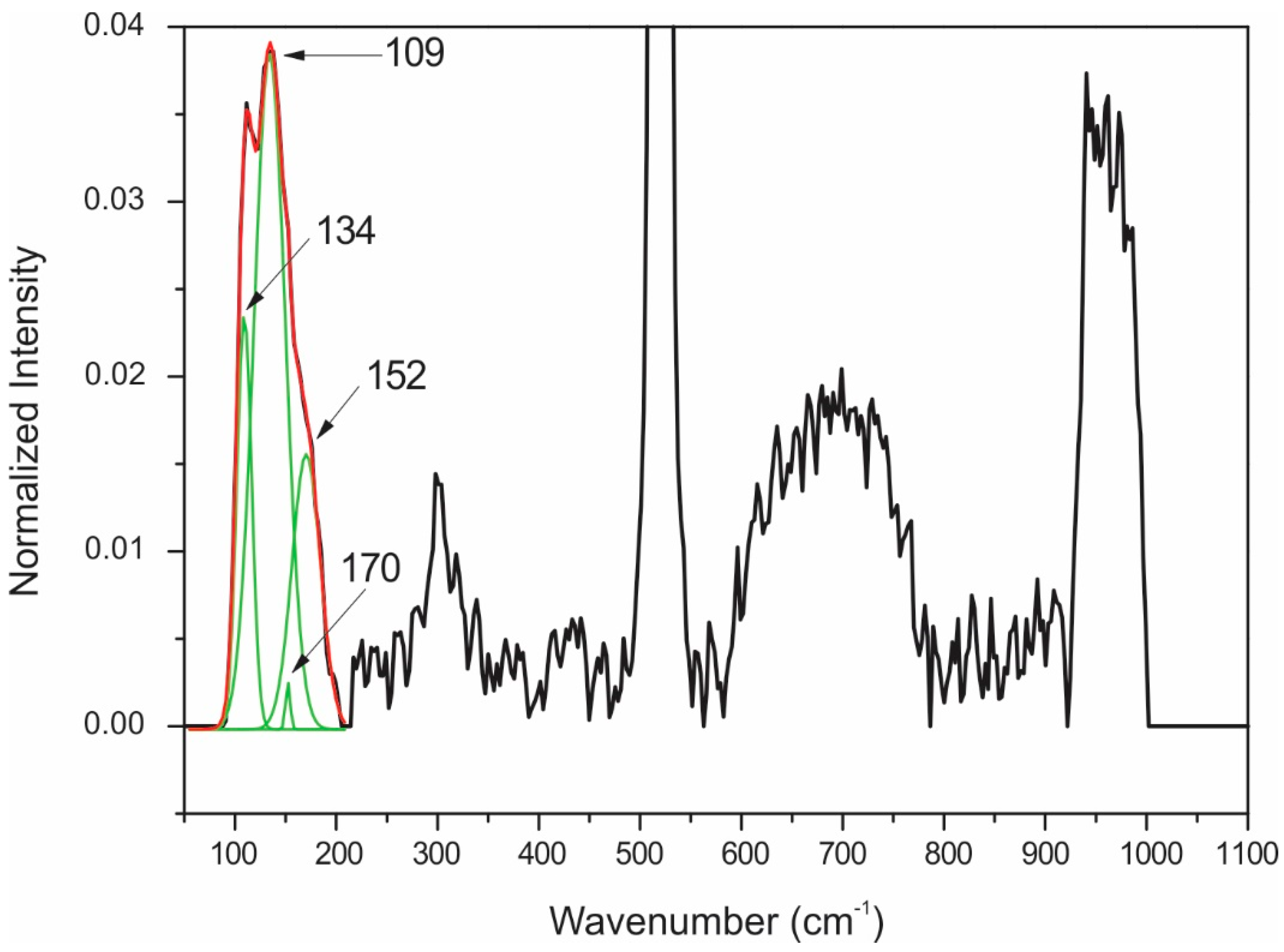
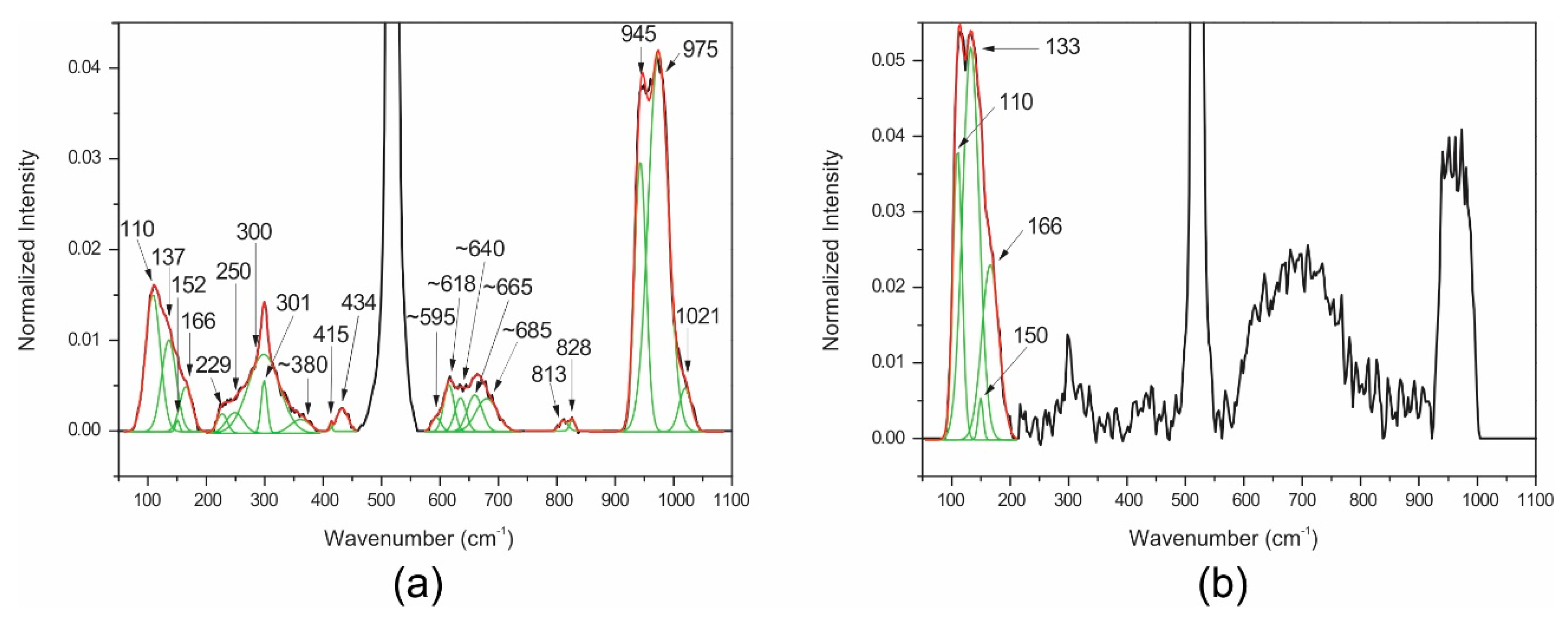
| 110 | AuTe2 | 110 | AuTe2 |
| 137 | AuTe2 | 133 | AuTe2 |
| 152 | AuTe2 | 150 | AuTe2 |
| 166 | AuTe2 | 166 | AuTe2 |
| 229 | α 2 | 229 | Unidentifiable (noisy signal) |
| 250 | α | 250 | Unidentifiable (noisy signal) |
| 300 | α | 300 | Unidentifiable (noisy signal) |
| ~380 | Te6+O6 ν2 bending | ~380 | Unidentifiable (noisy signal) |
| 415 | α | 415 | Unidentifiable (noisy signal) |
| 434 | Zn-O bending | 434 | Unidentifiable (noisy signal) |
| ~595 | α | ~595 | Unidentifiable (noisy signal) |
| ~618 | Te6+O6 ν1 symmetric stretching | ~618 | Unidentifiable (noisy signal) |
| ~640 | Te6+O6 ν3 antisymmetric stretching | ~640 | Unidentifiable (noisy signal) |
| ~665 | α | ~665 | Unidentifiable (noisy signal) |
| ~685 | Te6+O6 ν1 symmetric stretching | ~685 | Unidentifiable (noisy signal) |
| 813 | Si-O stretching | 813 | Unidentifiable (noisy signal) |
| 828 | Si-O stretching | 828 | Unidentifiable (noisy signal) |
| 945 | metasilicate | 945 | Unidentifiable (noisy signal) |
| 975 | Si-OH stretching | 975 | Unidentifiable (noisy signal) |
| 1021 | Si-O-Si bending | 1021 | Unidentifiable (noisy signal) |
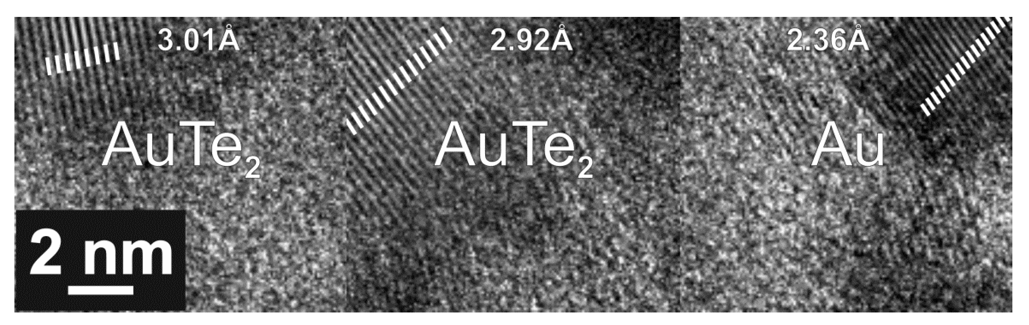
| dspacing 10 h (Å) | dspacing 20 h (Å 1) | Crystalline Phase | |||
|---|---|---|---|---|---|
| 3.24 ± 0.08 | α-TeO2 | ||||
| 3.13 ± 0.08 | ZnO | α-TeO2 | |||
| 2.98 ± 0.09 | 2.94 ± 0.07 | AuTe2 | ZnO | α-TeO2 | |
| 2.81 ± 0.07 | α-TeO2 | ||||
| 2.71 ± 0.07 | ZnO | α-TeO2 | |||
| 2.44 ± 0.09 | ZnO | ||||
| 2.35 ± 0.08 | 2.33 ± 0.06 | Au | ZnO | α-TeO2 | |
| 2.1 ± 0.06 | 2.07 ± 0.05 | AuTe2 | ZnO | α-TeO2 | |
| 2.01 ± 0.05 | Au | ||||
| 1.85 ± 0.03 | ZnO | α-TeO2 | |||
| 1.72 ± 0.03 | 1.7 ± 0.03 | AuTe2 | ZnO | ||
| 1.58 ± 0.02 | ZnO | ||||
| 1.54 ± 0.02 | AuTe2 | ||||
| 1.48 ± 0.02 | ZnO | ||||
| 1.43 ± 0.03 | Au | ||||
| 1.22 ± 0.02 | 1.23 ± 0.02 | Au | |||
| 1.18 ± 0.01 | Au | ZnO | |||
| 1 ± 0.01 | Au | ZnO | |||
| 0.932 ± 0.008 | Au | ||||
| 0.908 ± 0.007 | Au | ZnO | |||
© 2020 by the authors. Licensee MDPI, Basel, Switzerland. This article is an open access article distributed under the terms and conditions of the Creative Commons Attribution (CC BY) license (http://creativecommons.org/licenses/by/4.0/).
Share and Cite
Bontempo, L.; dos Santos Filho, S.G.; Kassab, L.R.P. Process Oxygen Flow Influence on the Structural Properties of Thin Films Obtained by Co-Sputtering of (TeO2)x-ZnO and Au onto Si Substrates. Nanomaterials 2020, 10, 1863. https://doi.org/10.3390/nano10091863
Bontempo L, dos Santos Filho SG, Kassab LRP. Process Oxygen Flow Influence on the Structural Properties of Thin Films Obtained by Co-Sputtering of (TeO2)x-ZnO and Au onto Si Substrates. Nanomaterials. 2020; 10(9):1863. https://doi.org/10.3390/nano10091863
Chicago/Turabian StyleBontempo, Leonardo, Sebastião G. dos Santos Filho, and Luciana R. P. Kassab. 2020. "Process Oxygen Flow Influence on the Structural Properties of Thin Films Obtained by Co-Sputtering of (TeO2)x-ZnO and Au onto Si Substrates" Nanomaterials 10, no. 9: 1863. https://doi.org/10.3390/nano10091863