Performance of Graphene–CdS Hybrid Nanocomposite Thin Film for Applications in Cu(In,Ga)Se2 Solar Cell and H2 Production

 , ,
, ,
Abstract
:
1. Introduction
2. Materials and Methods
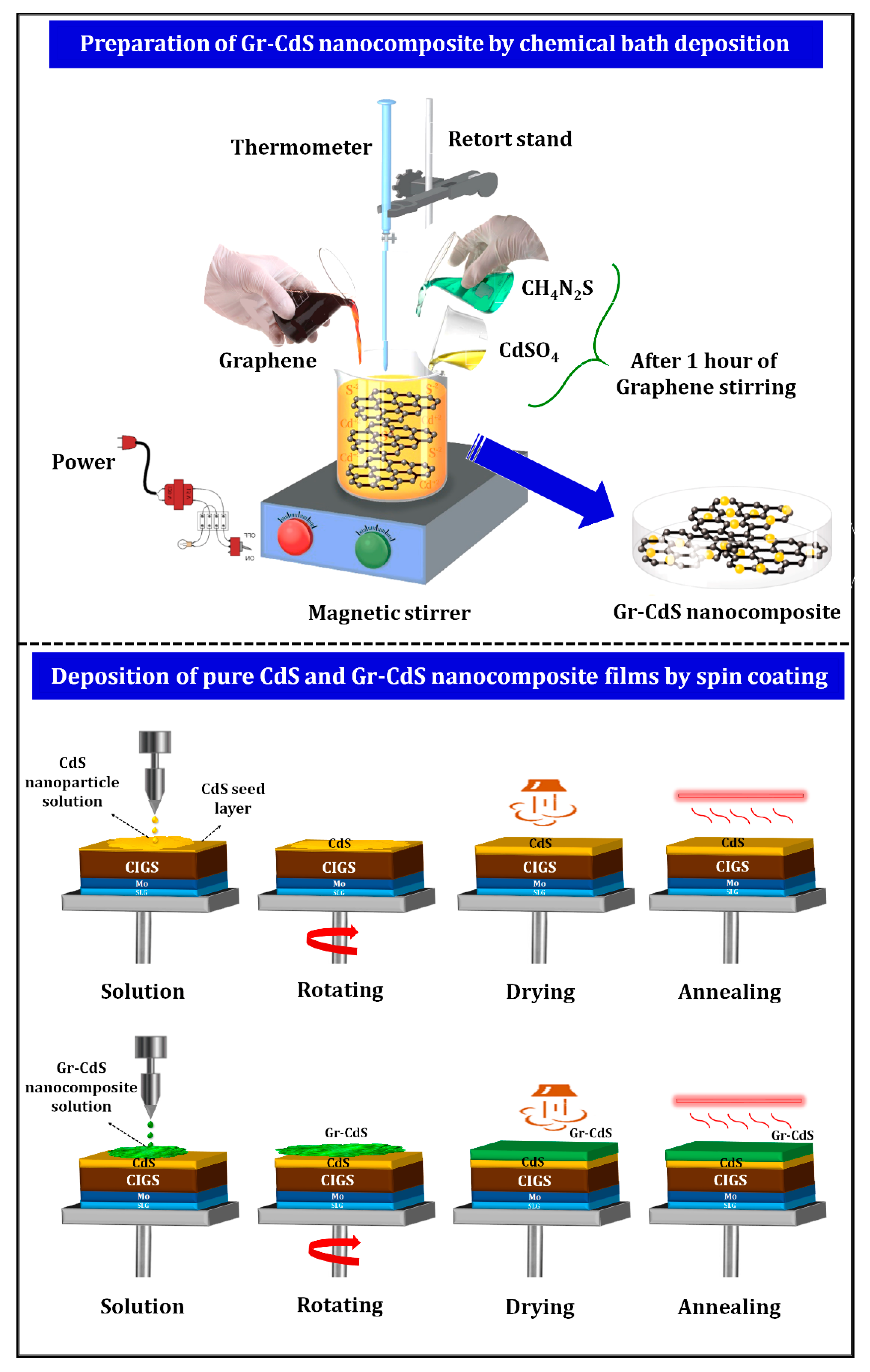
2.1. Synthesis of CdS NPs and Gr–CdS Nanocomposite
2.2. Film Preparation Using CdS NPs and Gr–CdS Nanocomposite
2.3. CIGS Device Fabrication
2.4. Characterization
2.4.1. Material Characterization
2.4.2. Solar Cell Characterization
2.4.3. PEC Measurement
3. Results
3.1. Properties of CdS NPs and Gr–CdS Nanocomposite
3.1.1. EDS Analysis
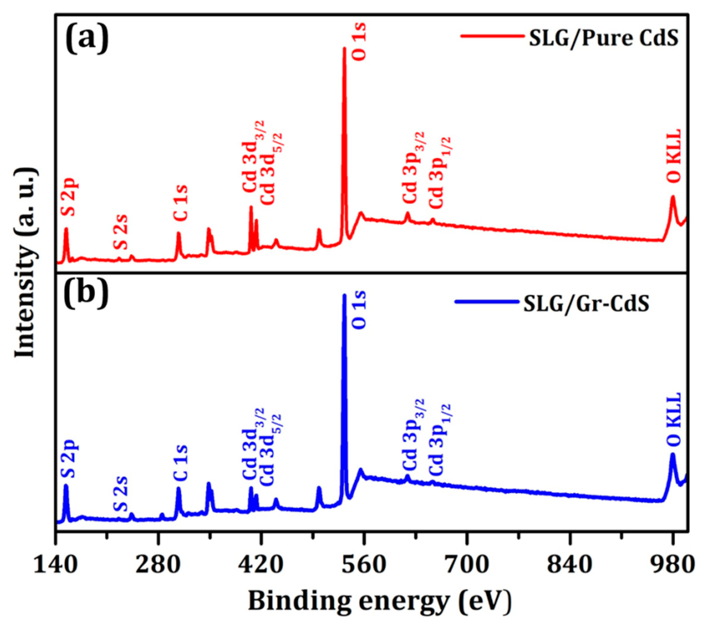
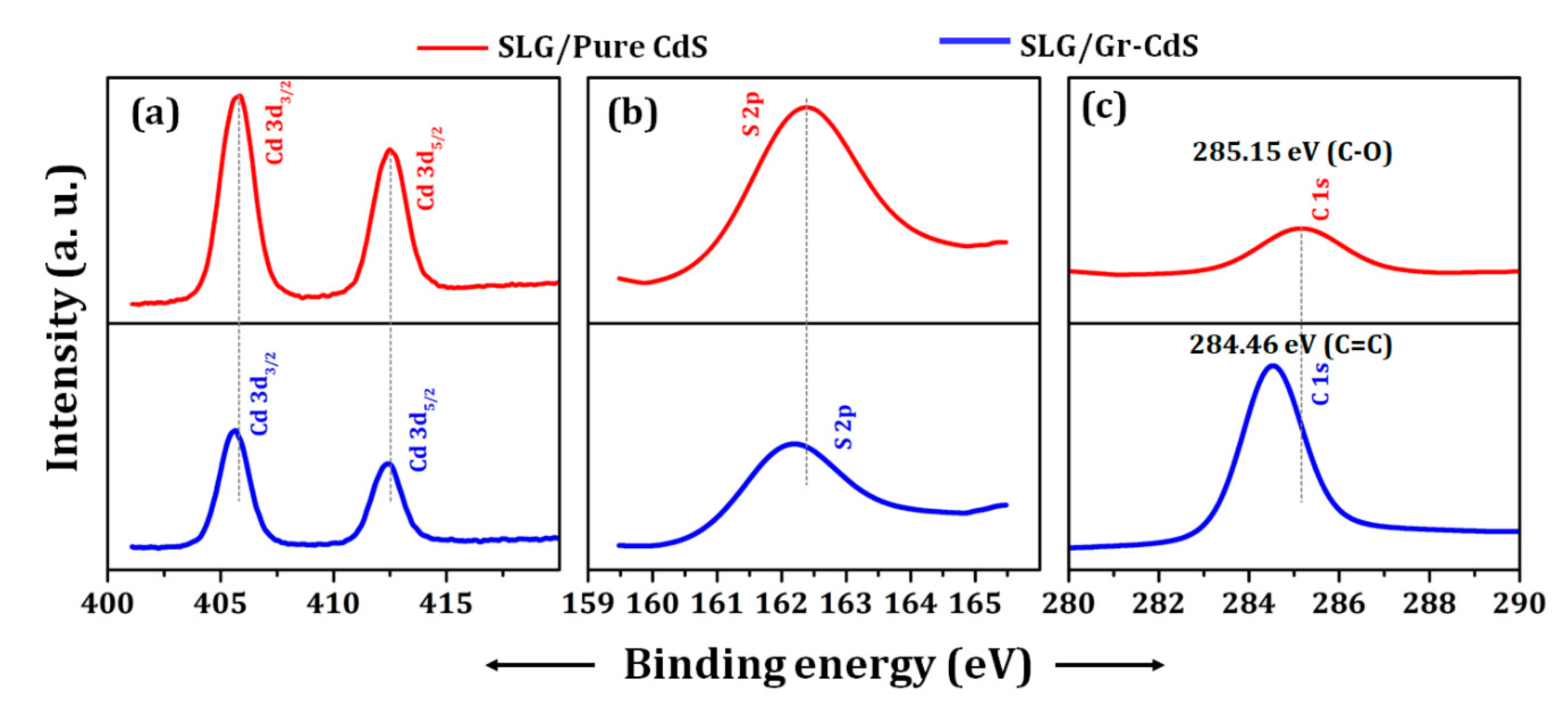
3.1.2. XPS Analysis
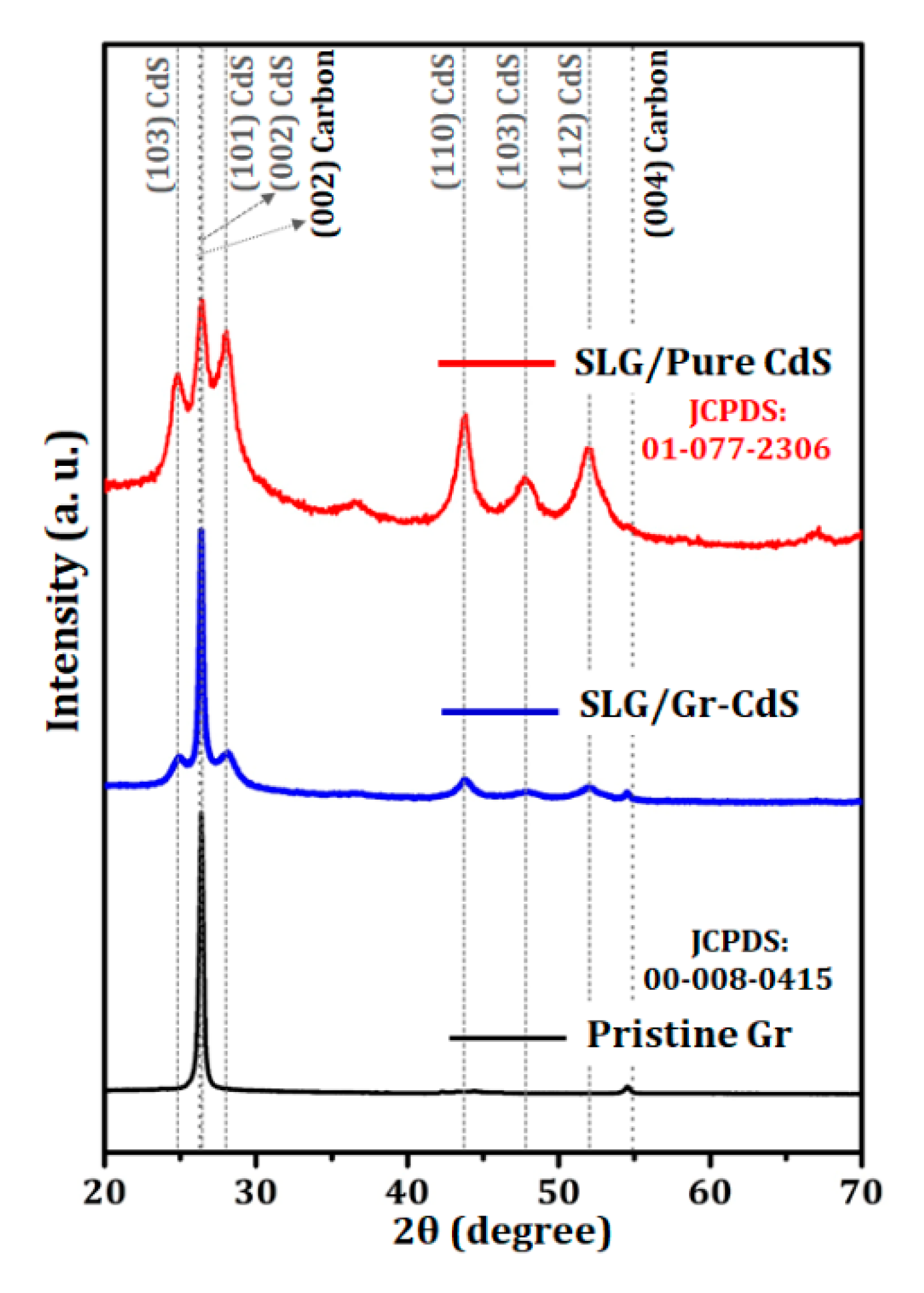
3.1.3. XRD Analysis
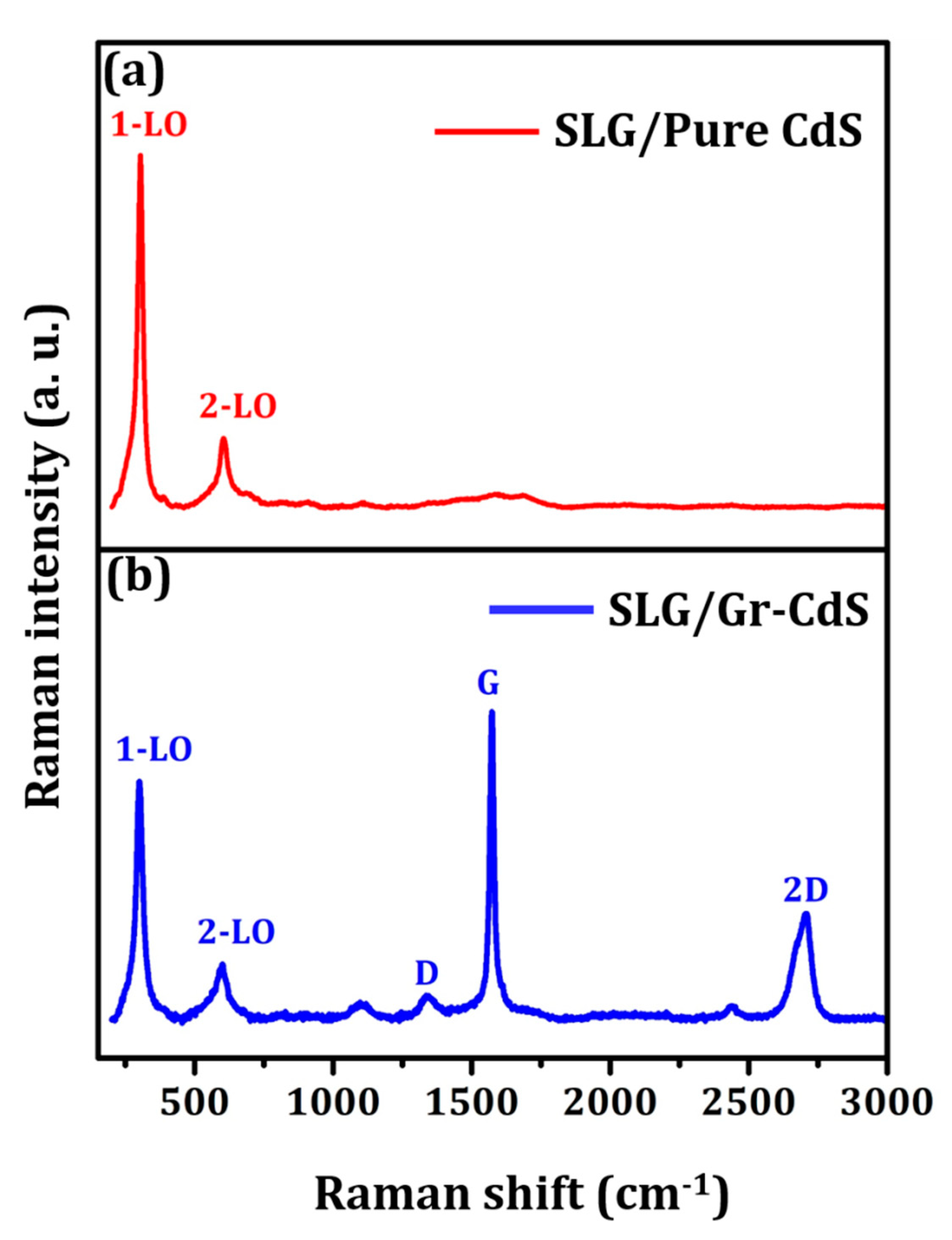
3.1.4. Raman Analysis
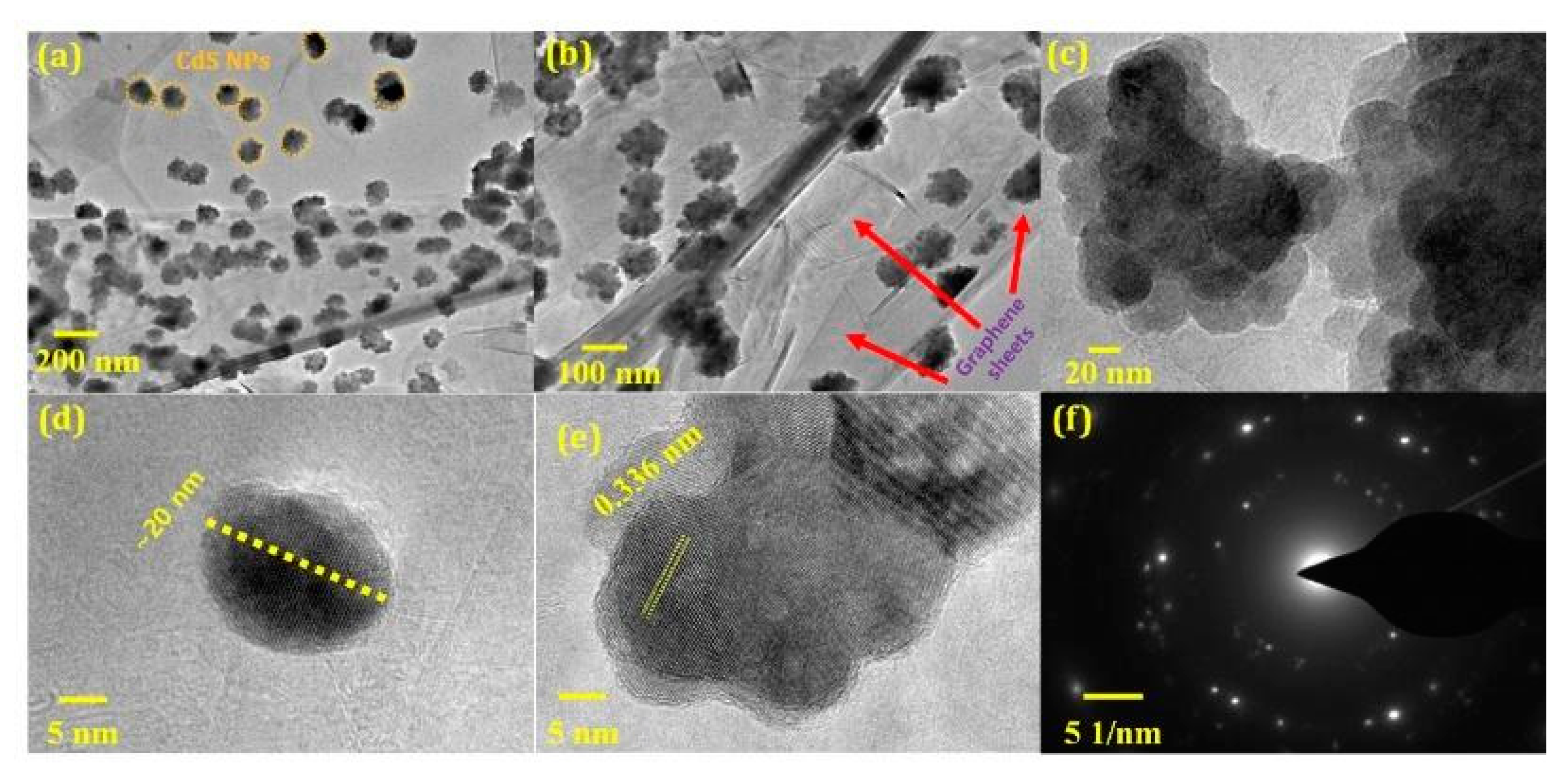
3.1.5. TEM Analysis
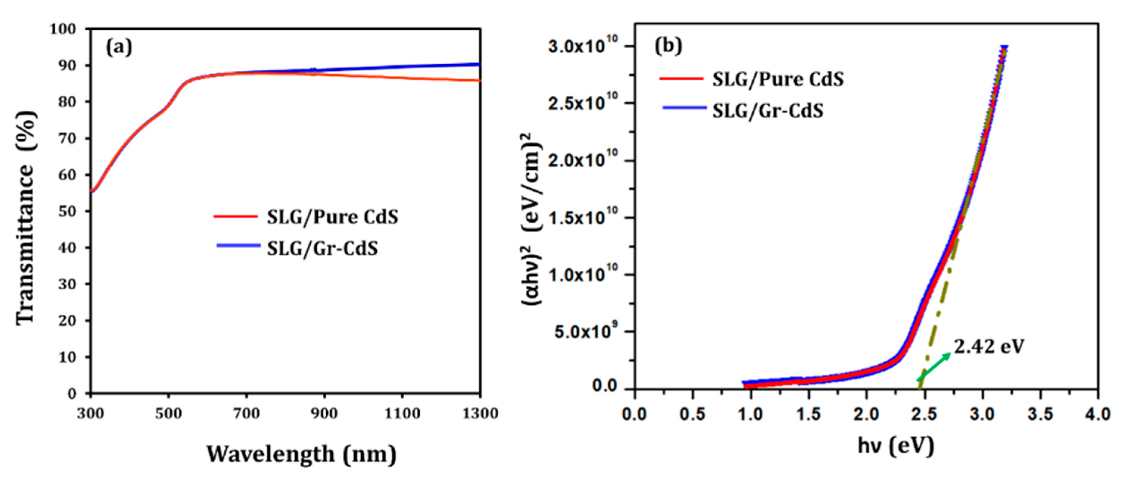
3.1.6. Optical Analysis
3.2. Applications of Pure CdS and SLG/Gr–CdS
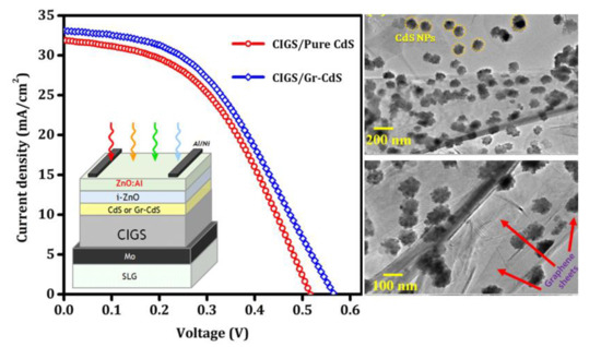
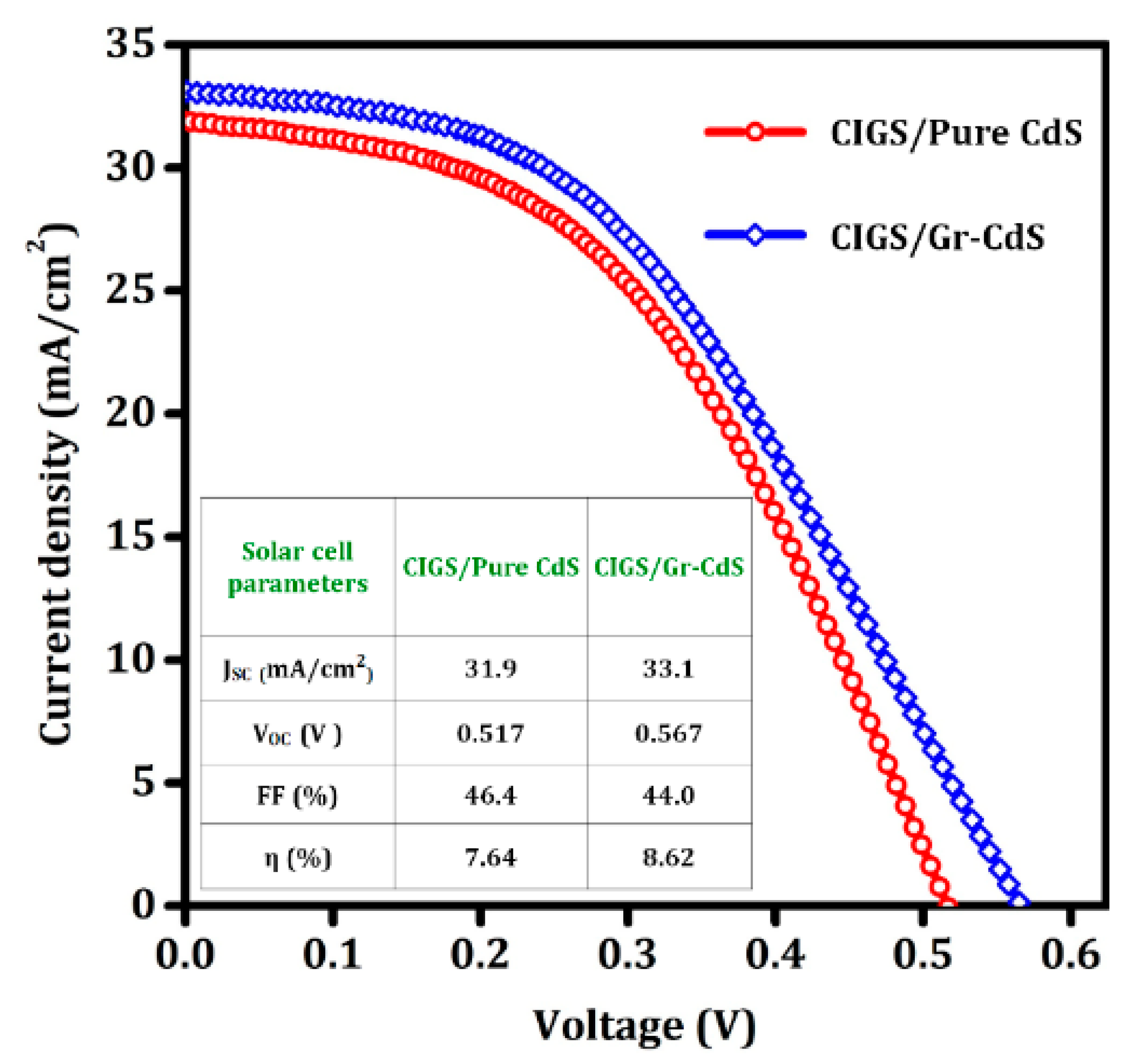
3.2.1. CIGS Photovoltaic Devices
3.2.2. Water Splitting
4. Conclusions
Author Contributions
Funding
Conflicts of Interest
References
- Leal-Cruz, A.L.; Vera-Marquina, A.; Berman-Mendoza, D.; VillaVelázquez-Mendoza, C.; Zaldívar-Huerta, I.E.; García-Delgado, L.A.; García-Juárez, A.R.; Gómez-Fuentes, A.; Rojas-Hernández, A.G. Microstructural and optical characterizations of highly stable nanospheres of crystalline CdS via selective approach. Opt. Mater. Express 2014, 4, 129–141. [Google Scholar] [CrossRef]
- Walker, B.; Kim, G.H.; Heo, J.; Chae, G.J.; Park, J.; Seo, J.H.; Kim, J.Y. Solution-processed CdS transistors with high electron mobility. RSC Adv. 2014, 4, 3153–3157. [Google Scholar] [CrossRef] [Green Version]
- Tedsana, W.; Tuntulani, T.; Ngeontae, W. A highly selective turn-on ATP fluorescence sensor based on unmodified cysteamine capped CdS quantum dots. Anal. Chim. Acta 2013, 783, 64–73. [Google Scholar] [CrossRef] [PubMed]
- Kirovskaya, I.A.; Filatova, T.N. Adsorption and electrophysical properties of semiconductors of the InSb-CdS system. Russ J Phys Chem A 2012, 86, 639–644. [Google Scholar] [CrossRef]
- Chopra, K.L.; Paulson, P.D.; Dutta, V. Thin-film solar cells: an overview. Progr. Photovoltaics Res. Appl. 2004, 12, 69–92. [Google Scholar]
- Alhammadi, S.; Moon, K.; Park, H.; Kim, W.K. Effect of different cadmium salts on the properties of chemical-bath-deposited CdS thin films and Cu(InGa)Se2 solar cells. Thin Solid Films 2017, 625, 56–61. [Google Scholar] [CrossRef]
- Chaure, N.B.; Bordas, S.; Samantilleke, A.P.; Chaure, S.N.; Haigh, J.; Dharmadasa, I.M. Investigation of electronic quality of chemical bath deposited cadmium sulphide layers used in thin film photovoltaic solar cells. Thin Solid Films 2003, 437, 10–17. [Google Scholar] [CrossRef]
- Cheng, L.; Xiang, Q.; Liao, Y.; Zhang, H. CdS-Based photocatalysts. Energy Environ. Sci. 2018, 11, 1362–1391. [Google Scholar] [CrossRef]
- Tso, S.; Li, W.S.; Wu, B.-H.; Chen, L.-J. Enhanced H2 production in water splitting with CdS-ZnO core-shell nanowires. Nano Energy 2018, 43, 270–277. [Google Scholar] [CrossRef]
- Fernández-Pérez, A.; Navarrete, C.; Valenzuela, P.; Gacitúa, W.; Mosquera, E.; Fernández, H. Characterization of chemically-deposited aluminum-doped CdS thin films with post-deposition thermal annealing. Thin Solid Films 2017, 623, 127–134. [Google Scholar] [CrossRef]
- Mukherjee, A.; Ghosh, P.; Aboud, A.A.; Mitra, P. Influence of copper incorporation in CdS: structural and morphological studies. Mater. Chem. Phys. 2016, 184, 101–109. [Google Scholar] [CrossRef]
- Patel, N.H.; Deshpande, M.P.; Chaki, S.H. Study on structural, magnetic properties of undoped and Ni doped CdS nanoparticles. Mater. Sci. Semicond. Process. 2015, 3, 272–280. [Google Scholar] [CrossRef]
- Mageswari, S.; Dhivya, L.; Palanivel, B.; Murugan, R. Structural, morphological and optical properties of Na and K dual doped CdS thin film. J. Alloys. Compd. 2012, 545, 41–45. [Google Scholar] [CrossRef]
- Alhammadi, S.; Jung, H.; Kwon, S.; Park, H.; Shim, J.-J.; Cho, M.H.; Lee, M.; Kim, J.S.; Kim, W.K. Effect of Gallium doping on CdS thin film properties and corresponding Cu(InGa)Se2/CdS: Ga solar cell performance. Thin Solid Films 2018, 660, 207–212. [Google Scholar] [CrossRef]
- Gode, F. Effect of Cu doping on CdS as a multifunctional nanomaterial: Structural, morphological, optical and electrical properties. Optic 2019, 197, 163217. [Google Scholar] [CrossRef]
- Kaur, M.; Kaur, M.; Sharma, V.K. Nitrogen-doped graphene and graphene quantum dots: A review onsynthesis and applications in energy, sensors and environment. Adv. Colloid Interface Sci. 2018, 259, 44–64. [Google Scholar] [CrossRef]
- Chang, C.-Y.; Ju, S.P.; Chang, S.; Huang, J.-W.; Yang, S.-C.; Yang, H.-W. The thermal conductivity and mechanical properties of poly(p-phenylene sulfide)/oxided-graphene and poly(p-phenylene sulfide)/defect-graphene nano-composites by molecular dynamics simulation. RSC Adv. 2014, 4, 26074–26080. [Google Scholar] [CrossRef]
- Biccari, F.; Gabelloni, F.; Burzi, E.; Gurioli, M.; Pescetelli, S.; Agresti, A.; Del Rio Castillo, A.E.; Ansaldo, A.; Kymakis, E.; Bonaccorso, F.; et al. Graphene-based electron transport layers in perovskite solar cells: a step-up for an efficient Carrier collection. Adv. Energy Mater. 2017, 7, 1701349. [Google Scholar] [CrossRef]
- Bi, H.; Huang, F.; Liang, J.; Xie, X.; Jiang, M. Transparent conductive graphene films synthesized by ambient pressure chemical vapor deposition used as the front electrode of CdTe solar cells. Adv. Mater. 2011, 23, 3202–3206. [Google Scholar] [CrossRef]
- Lin, T.; Huang, F.; Liang, J.; Wang, Y. A facile preparation route for boron-doped graphene, and its CdTe solar cell application. Energy Environ. Sci. 2011, 4, 862–865. [Google Scholar] [CrossRef]
- Bi, X.; Luo, G.; Li, W.; Zhang, J.; Wu, L.; Li, B.; Zeng, G.; Wang, W. Bi-containing reduced graphene oxide for CdTe solar cells. Sol. Energy 2017, 170, 820–827. [Google Scholar] [CrossRef]
- Yin, L.; Zhang, K.; Luo, H.; Cheng, G.; Ma, X.; Xiong, Z.; Xiao, X. Highly efficient graphene-based Cu(In, Ga)Se2 solar cells with large active area. Nanoscale 2014, 6, 10879–10886. [Google Scholar] [CrossRef] [PubMed]
- Sim, J.-K.; Kang, S.; Nandi, R.; Jo, J.-Y.; Jeong, K.-U.; Lee, C.-R. Implementation of graphene as hole transport electrode in flexible CIGS solar cells fabricated on Cu foil. Sol. Energy 2018, 162, 357–363. [Google Scholar] [CrossRef]
- Ryu, H.; Park, D.H.; Jung, Y.; Kim, J.; Kim, W.K. Control of the Preferred Orientation of Polycrystalline Mo and Cu(InGa)Se2 Thin Films by Inserting Graphene Layer. Sci. Adv. Mater. 2018, 10, 570–574. [Google Scholar] [CrossRef]
- Nouri, E.; Wang, Y.-L.; Chen, Q.; Xu, J.-J.; Paterakis, G.; Dracopoulos, V.; Xu, Z.-X.; Tasis, D.; Mohammadi, M.R.; Lianos, P. Introduction of Graphene oxide as Buffer layer in perovskite solar cells and the promotion of soluble n-Buthyl-substituted copper phthalocyanine as efficient hole transporting material. Electrochim. Acta 2017, 233, 36–43. [Google Scholar] [CrossRef] [Green Version]
- Liu, Z.; You, P.; Xie, C.; Tang, G.; Yan, F. Ultrathin and flexible perovskite solar cells with graphene transparent electrodes. Nano Energy 2016, 28, 151–157. [Google Scholar] [CrossRef]
- Hu, X.; Jiang, H.; Li, J.; Ma, J.; Yang, D.; Liu, Z.; Gao, F.; Liu, S.F. Air and thermally stable perovskite solar cells with CVD-graphene as the blocking layer. Nanoscale 2017, 9, 8274–8280. [Google Scholar] [CrossRef]
- Chen, S.; Xu, Y.; Li, C.; Xiao, X.; Chen, Y. Modification of N-doped graphene films and their applications in heterojunction solar cells. Sol. Energy 2018, 174, 66–72. [Google Scholar] [CrossRef]
- Yavuz, S.; Kuru, C.; Choi, D.; Kargar, A.; Jin, S.; Bandaru, P.R. Graphene oxide as a p-dopant and an anti-reflection coating layer, in graphene/silicon solar cells. Nanoscale 2016, 8, 6473–6478. [Google Scholar] [CrossRef]
- Selopal, G.S.; Milan, R.; Ortolani, L.; Morandi, V.; Rizzoli, R.; Sberveglieri, G.; Veronese, G.P.; Vomiero, A.; Concina, I. Graphene as transparent front contact for dye sensitized solar cells. Sol. Energy Mater. Sol. Cells 2015, 135, 99–105. [Google Scholar] [CrossRef]
- Wang, Z.; Wang, C.; Qian, M.; Li, Z.; Qiu, H. Preparation of well-proportioned SnS hollow microsphere on graphene and the application in dye-sensitized solar cells. Mater. Lett. 2018, 233, 344–347. [Google Scholar] [CrossRef]
- Shin, D.H.; Seo, S.W.; Kim, J.M.; Lee, H.S.; Choi, S.-H. Graphene transparent conductive electrodes doped with graphene quantum dots-mixed silver nanowires for highly-flexible organic solar cells. J. Alloys Compd. 2018, 744, 1–6. [Google Scholar] [CrossRef]
- Gomez De Arco, L.; Zhang, Y.; Schlenker, C.W.; Ryu, K.; Thompson, M.E.; Zhou, C. Continuous, highly flexible, and transparent graphene films by chemical vapor deposition for organic photovoltaics. ACS Nano 2010, 4, 2865–2873. [Google Scholar] [CrossRef] [PubMed]
- Ansari, Z.A.; Singh, T.J.; Islam, S.M.; Singh, S.; Mahala, P.; Khan, A.; Singh, K.J. Photovoltaic solar cells based on graphene/gallium arsenide Schottky junction. Optik 2019, 182, 500–506. [Google Scholar] [CrossRef]
- Chen, Z.; Liu, S.; Yang, M.-Q.; Xu, Y.-J. Synthesis of uniform CdS nanospheres/graphene hybrid nanocomposites and their application as visible light photocatalyst for selective reduction of nitro organics in water. ACS Appl. Mater. Interfaces 2013, 5, 4309–4319. [Google Scholar] [CrossRef]
- Deng, C.-H.; Gang, J.-L.; Zeng, G.-M.; Jiang, Y.; Zhang, C.; Liu, H.-Y.; Huan, S.-Y. Graphene-CdS nanocomposite inactivation performance toward Escherichia coli in the presence of humic acid under visible light irradiation. Chem. Eng. J. 2016, 284, 41–53. [Google Scholar] [CrossRef]
- Xiao, F.X.; Miao, J.; Liu, B. Layer-by-Layer Self-Assembly of CdS Quantum Dots/Graphene Nanosheets Hybrid Films for Photoelectrochemical and Photocatalytic Applications. J. Am. Chem. Soc. 2014, 136, 1559–1569. [Google Scholar] [CrossRef]
- Wang, Z.; Liu, Z.; Chen, J.; Yang, H.; Luo, J.; Gao, J.; Zhang, J.; Yang, C.; Jia, S.; Liu, B. Self-assembly of three-dimensional CdS nanosphere/graphene networks for efficient photocatalytic hydrogen evolution. J Energy Chem. 2019, 31, 34–38. [Google Scholar] [CrossRef] [Green Version]
- Khan, M.E.; Khan, M.M.; Cho, M.H. CdS–graphene nanocomposite for efficient visible-light-driven photocatalytic and photoelectrochemical applications. J. Colloid Interface Sci. 2016, 482, 221–230. [Google Scholar] [CrossRef]
- Yang, G.; Yang, B.; Xiao, T.; Yan, Z. One-step solvothermal synthesis of hierarchically porous nanostructured CdS/TiO2 heterojunction with higher visible light photocatalytic activity. Appl. Surf. Sci. 2013, 283, 402–410. [Google Scholar] [CrossRef]
- Wang, H.; Gupta, A.; Kim, B.S. Photo-crosslinked polymer networks based on graphene-functionalized soybean oil and their properties. Korean J. Chem. Eng. 2019, 36, 591–599. [Google Scholar] [CrossRef]
- Ha, H.; Ellison, C.J. Polymer/graphene oxide (GO) thermoset composites with GO as a crosslinker. Korean J. Chem. Eng. 2018, 35, 303–317. [Google Scholar] [CrossRef]
- Guan, Y.; Hu, T.; Wu, J.; Zhao, L.; Tian, F.; Pan, W.; He, P.; Qi, X.; Li, F.; Xu, K. Enhanced photocatalytic activity of TiO2/graphene by tailoring oxidation degrees of graphene oxide for gaseous mercury removal. Korean J. Chem. Eng. 2019, 36, 115–125. [Google Scholar] [CrossRef]
- Ren, Z.; Zhang, J.; Xiao, F.-X.; Xiao, G. Revisiting the construction of graphene–CdS nanocomposites as efficient visible-light-driven photocatalysts for selective organic transformation. J. Mater. Chem. A 2014, 2, 5330–5339. [Google Scholar] [CrossRef]
- Dai, Z.; Zhang, J.; Bao, J.; Huang, X.; Mo, X. Facile synthesis of high-quality nano-sized CdS hollow spheres and their application in electrogenerated chemiluminescence sensing. J. Mater. Chem. 2007, 17, 1087–1093. [Google Scholar] [CrossRef]
- Graf, D.; Molitor, F.; Ensslin, K.; Stampfer, C.; Jungen, A.; Hierold, C.; Wirtz, L. Spatially resolved Raman spectroscopy of single- and few-layer graphene. Nano Lett. 2007, 7, 238–242. [Google Scholar] [CrossRef] [PubMed] [Green Version]
- Calizo, A.; Balandin, A.A.; Bao, W.; Miao, F.; Lau, C. Temperature dependence of the Raman spectra of graphene and graphene multilayers. Nano Lett. 2007, 7, 2645–2649. [Google Scholar] [CrossRef]
- Ghaemi, F.; Yunus, R.; Ahmadian, A.; Ismail, F.; Salleh, M.A.M.; Rashid, S.A. Few- and multi-layer graphene on carbon fibers: synthesis and application. RSC Adv. 2015, 5, 81266–81274. [Google Scholar] [CrossRef]
- Ferrari, A.C. Raman spectroscopy of graphene and graphite: disorder, electron–phonon coupling, doping and nonadiabatic effects. Solid State Commun. 2007, 143, 47–57. [Google Scholar] [CrossRef]
- Gao, Z.; Liu, N.; Wu, D.; Tao, W.; Xu, F.; Jiang, K. Graphene–CdS composite, synthesis and enhanced photocatalytic activity. Appl. Surf. Sci. 2012, 258, 2473–2478. [Google Scholar] [CrossRef]
- Zhu, W.; Low, T.; Perebeinos, V.; Bol, A.A.; Zhu, Y.; Yan, H.; Tersoff, J.; Avouris, P. Structure and electronic transport in graphene wrinkles. Nano Lett. 2012, 12, 3431–3436. [Google Scholar]
- Yue, G.; Wu, J.; Xiao, Y.; Huang, M.; Lin, J.; Fan, L.; Lan, Z. Platinum/graphene hybrid film as a counter electrode for dye-sensitized solar cells. Electrochim. Acta 2013, 92, 64–70. [Google Scholar] [CrossRef]
- Hwang, S.; Kim, D.; Kim, M.; Baek, D.; Park, J.-H.; Song, W.; Shim, J.-P.; Lee, J. Influence of Cadmium Sources on Properties of Chemically Deposited Cadmium Sulfide Thin Films for Highly Efficient Cu(In,Ga)(Se,S)2 Solar Cells. Sci. Adv. Mater. 2018, 10, 139–143. [Google Scholar] [CrossRef]
- Bell, N.J.; Ng, Y.H.; Du, A.; Coster, H.; Smith, S.C.; Amal, R. Understanding the enhancement in photoelectrochemical properties of photocatalytically prepared TiO2-reduced graphene oxide composite. J. Phys. Chem. C 2011, 115, 6004–6009. [Google Scholar] [CrossRef]
- Manikandan, V.S.; Palai, A.K.; Mohanty, S.; Nayak, S.K. Hydrothermally synthesized self-assembled multi-dimensional TiO2/Graphene oxide composites with efficient charge transfer kinetics fabricated as novel photoanode for dye sensitized solar cell. J. Alloys. Compd. 2019, 793, 400–409. [Google Scholar] [CrossRef]
- Sookhakian, M.; Amin, Y.M.; Basirun, W.J. Hierarchically ordered macro-mesoporous ZnS microsphere with reduced graphene oxide supporter for a highly efficient photodegradation of methylene blue. Appl. Surf. Sci. 2013, 283, 668–677. [Google Scholar] [CrossRef]
- Lei, Y.; Li, R.; Chen, F.; Xu, J. Hydrothermal synthesis of graphene–CdS composites with improved photoelectric characteristics. J. Mater Sci. Mater Electron 2014, 25, 3057–3061. [Google Scholar] [CrossRef]
- Chakrabarty, S.; Mukherjee, A.; Basu, S. RGO-MoS2 Supported NiCo2O4 Catalyst towards Solar Water Splitting and Dye Degradation. ACS Sustainable Chem. Eng. 2018, 6, 5238–5247. [Google Scholar] [CrossRef]
- Dandan, L.; Min, Z.; Zhihua, Z.; Qiuye, L.; Xiaodong, W.; Jianjun, Y. Self-organized vanadium and nitrogen co-doped titania nanotube arrays with enhanced photocatalytic reduction of CO2 into CH4. Nanoscale Research Letters. 2014, 9, 272. [Google Scholar]
- Rajeshwar, K. Hydrogen generation at irradiated oxide semiconductor solution interfaces. J Appl Electrochem. 2007, 37, 765–787. [Google Scholar] [CrossRef]
- Zhou, Q.; Lin, Y.; Zhang, K.; Li, M.; Tang, D. Reduced graphene Oxide/BiFeO3 nanohybrids-based signal-on photoelectrochemical sensing system for prostate-specific antigen detection coupling with magnetic microfluidic device. Biosens. Bioelectron. 2018, 101, 146–152. [Google Scholar] [CrossRef] [PubMed]
- Ye, A.; Fan, W.; Zhang, Q.; Deng, W.; Wang, Y. CdS–graphene and CdS–CNT nanocomposites as visible-light photocatalysts for hydrogen evolution and organic dye degradation. Catal. Sci. Technol. 2012, 2, 969–978. [Google Scholar] [CrossRef]
- Chang, K.; Mei, Z.W.; Wang, T.; Kang, Q.; Ouyang, S.X.; Ye, J.H. MoS2/graphene cocatalyst for efficient photocatalytic H2 evolution under visible light irradiation. ACS Nano 2014, 8, 7078–7087. [Google Scholar] [CrossRef] [PubMed]
- Han, W.; Ren, L.; Qi, X.; Liu, Y.; Wei, X.; Huang, Z.; Zhong, J. Synthesis of CdS/ZnO/graphene composite with high-efficiency photoelectrochemical activities under solar radiation. Appl. Surf. Sci. 2014, 299, 12–18. [Google Scholar] [CrossRef]
- Liu, M.; Li, F.; Sun, Z.; Ma, L.; Xu, L.; Wang, Y. Noble-metal-free photocatalysts MoS2-graphene/CdS mixed nanoparticles/nanorods morphology with high visible light efficiency for H2. evolution Chem. Commun. 2014, 50, 11004–11007. [Google Scholar] [CrossRef]
- Jia, L.; Wang, D.; Huang, Y.; Xu, A.; Yu, H. Highly durable N-doped graphene/CdS nanocomposites with enhanced photocatalytic hydrogen evolution from water under visible light irradiation. J. Phys. Chem. C 2011, 115, 11466–11473. [Google Scholar] [CrossRef]
- Liu, H.; Lv, T.; Wu, X.; Zhu, C.; Zhu, Z. Preparation and enhanced photocatalytic activity of CdS@RGO core-shell structural microspheres. Appl. Surf. Sci. 2014, 305, 242–246. [Google Scholar] [CrossRef]
- Ye, H.; Wang, H.; Zhao, F.; Zeng, B. A one-pot hydrothermal synthesis of graphene/CdS:Mn photocatalyst for photoelectrochemical sensing of glutathione. RSC Adv. 2017, 7, 45792–45798. [Google Scholar] [CrossRef] [Green Version]
- Huang, Y.; Chen, Y.; Hu, C.; Zhang, B.; Shen, T.; Chen, X.; Zhang, M.Q. ‘Bridge’ effect of CdS nanoparticles in the interface of graphene-polyaniline composites. J. Mater. Chem. 2012, 22, 10999–11002. [Google Scholar] [CrossRef]


| Solar Cell Type | Graphene Type | Graphene Deposition Method | Role of Graphene | Photovoltaic Parameters | Ref. | |||
|---|---|---|---|---|---|---|---|---|
| Jsc(mA/cm2) | Voc(V) | FF(%) | Efficiency(%) | |||||
| CdTe | Gr | CVD | Front electrode | 22.9 | 0.430 | 42.0 | 4.17 | [19] |
| B:Gr | Solution method | Back electrode | 22.0 | 0.685 | 52.2 | 7.86 | [20] | |
| Bi:RGO | Hummers method | 26.2 | 0.787 | 63.7 | 13.2 | [21] | ||
| CIGS | Au:Gr | CVD | Front electrode | 32.4 | 0.601 | 69.1 | 13.5 | [22] |
| Gr | Back electrode | 28.8 | 0.531 | 64.7 | 9.91 | [23] | ||
| Mo/Gr back electrode | - | - | - | - | [24] | |||
| PSC | GO | Hummers method | Buffer layer | 20.9 | 1.04 | 66.0 | 14.4 | [25] |
| Gr | CVD | Front electrode | 18.6 | 1.04 | 59.4 | 11.5 | [26] | |
| Gr | Blocking layer | 21.1 | 1.09 | 68.2 | 15.7 | [27] | ||
| n-Si | N-doped Gr | Front electrode | 30.9 | 0.490 | 41.2 | 6.24 | [28] | |
| GO | Hummers method | Antireflection | 38.4 | 0.512 | 53.0 | 10.6 | [29] | |
| DSSC | Gr | CVD | Front electrode | 7.80 | 0.630 | 40.0 | 2.0 | [30] |
| SnS@RGO | Solution method | Counter electrode | 18.9 | 0.705 | 57.9 | 8.21 | [31] | |
| OSC | Gr doped with GQDs and Ag NWs | CVD | Front electrode | 10.4 | 0.592 | 59.3 | 3.66 | [32] |
| Gr | 4.73 | 0.480 | 52.0 | 1.18 | [33] | |||
| GaAs | Gr | Simulation | Formation of Schottky junction | 2.14 | 0.350 | 69.7 | 5.3 | [34] |
| Material | Cd (at%) | S (at%) | C (at%) | Cd/S (-) |
|---|---|---|---|---|
| Pure CdS | 47.6 | 52.4 | 0.0 | 0.91 |
| Gr-CdS | 10.7 | 11.5 | 77.8 | 0.93 |
| Material Structure | Preparation Method | Experiment Condition | Electrolyte | Current Density (μA/cm2) | Ref. |
|---|---|---|---|---|---|
| Gr–CdS | Hydrothermal | 180 °C, 40 h | 0.5 M Na2SO4 | 55 | [62] |
| Hydrothermal | 140 °C, 24 h | 0.2 M Na2SO4 | 12 | [35] | |
| Chemical precipitation | 25 °C, 48 h | 0.25 M Na2S and 0.35 M Na2SO3 | 120 | [63] | |
| Hydrothermal | 200 °C, 6 h | 0.24 M Na2S and 0.35 M Na2SO3 | 45 | [64] | |
| Hydrothermal | 120 °C, 12 h | 0.1 M H2SO4 | 15 | [57] | |
| Hydrothermal | 180 °C, 12 h | 0.1 M Na2SO4 | 0.01 | [65] | |
| N-graphene/CdS | Hydrothermal | 25 °C, 48 h | 0.5 M Na2SO4 | 40 | [66] |
| RGO–CdS | Hydrothermal | 120 °C, 48 h | -- | 9 | [67] |
| ITO/Gr–CdS:Mn | Hydrothermal | 200 °C, 12 h | 0.1 M Na2SO4 | 15 | [68] |
| Gr–CdS–PANI-6 | Hydrothermal | 70 °C, 6 h | 0.1 M KCl | 0.4 | [69] |
| Gr-–CdS | Chemical precipitation | 25 °C, 2 h | 0.5 M Na2SO4 | 40 | This work |
© 2020 by the authors. Licensee MDPI, Basel, Switzerland. This article is an open access article distributed under the terms and conditions of the Creative Commons Attribution (CC BY) license (http://creativecommons.org/licenses/by/4.0/).
Share and Cite
Alhammadi, S.; Minnam Reddy, V.R.; Gedi, S.; Park, H.; Sayed, M.S.; Shim, J.-J.; Kim, W.K. Performance of Graphene–CdS Hybrid Nanocomposite Thin Film for Applications in Cu(In,Ga)Se2 Solar Cell and H2 Production. Nanomaterials 2020, 10, 245. https://doi.org/10.3390/nano10020245
Alhammadi S, Minnam Reddy VR, Gedi S, Park H, Sayed MS, Shim J-J, Kim WK. Performance of Graphene–CdS Hybrid Nanocomposite Thin Film for Applications in Cu(In,Ga)Se2 Solar Cell and H2 Production. Nanomaterials. 2020; 10(2):245. https://doi.org/10.3390/nano10020245
Chicago/Turabian StyleAlhammadi, Salh, Vasudeva Reddy Minnam Reddy, Sreedevi Gedi, Hyeonwook Park, Mostafa Saad Sayed, Jae-Jin Shim, and Woo Kyoung Kim. 2020. "Performance of Graphene–CdS Hybrid Nanocomposite Thin Film for Applications in Cu(In,Ga)Se2 Solar Cell and H2 Production" Nanomaterials 10, no. 2: 245. https://doi.org/10.3390/nano10020245