InP-Based Foundry PICs for Optical Interconnects
by
 , and
, and
Francisco M. Soares
* ,
,
Moritz Baier
,
Tom Gaertner
,
Norbert Grote
,
Martin Moehrle
,
Tobias Beckerwerth
,
Patrick Runge
and
Martin Schell
Fraunhofer Heinrich Hertz Institute, 10587 Berlin, Germany
*
Author to whom correspondence should be addressed.
Appl. Sci. 2019, 9(8), 1588; https://doi.org/10.3390/app9081588
Submission received: 25 February 2019
/
Revised: 9 April 2019
/
Accepted: 9 April 2019
/
Published: 17 April 2019
(This article belongs to the Special Issue PICs for Optical Interconnects)
Abstract
:This paper describes a fabrication process for realizing Indium-Phosphide-based photonic-integrated circuits (PICs) with a high level of integration to target a wide variety of optical applications. To show the diversity in PICs achievable with our open-access foundry process, we illustrate two examples: a fully-integrated 20 Gb/s dual-polarization electro-absorption-modulated laser, and a balanced detector composed of avalanche photodiodes for detection of 28 Gb/s optical signals. On another note, datacenters are increasingly relying on hybrid integration of PICs from different technology platforms to increase transmission capacity, while simultaneously lowering cost, size, and power consumption. Several technology platforms require surface coupling rather than the traditional edge coupling to couple the light from one PIC to another. To accommodate the surface-coupling approach in our integration platform, we have developed a strategy to transfer the following optical Input/Output devices into our fabrication process: grating couplers, and vertical mirrors. In addition, we introduced etched facets into the process to improve the usability of our edge-coupling elements. We believe that the additional flexibility in Input/Output interfacing combined with the integration of multiple devices onto one PIC to reduce the number of PIC-to-PIC alignments can contribute significantly to the development of compact, low-cost, and high-performance datacenter modules.
1. Introduction
Optical Interconnects and photonic integration are currently gaining a lot of attention in the optical communications community. The telecommunications market is gearing up towards a huge increase in human connectivity, but also in human-to-machine- and machine-to-machine connectivity (5G, cloud-computing services, IoT, Industry 4.0, car-to-car communications, video connectivity, etc.) [1]. Datacenters are expected to play an increasingly bigger role, and the associated traffic is expected to increase dramatically for both the traditional intra-datacenter fiber-optic links from server to server (the so-called east-west traffic), but also for the inter-datacenter fiber-optic links from one datacenter to another (the north-south traffic) [2,3,4]. The main factors driving deployment of ultra-high-capacity fiber-optic links (such as 400G) in datacenters are cost, size, and power consumption. Fiber-optic links in datacenters today rely on compact- and low-cost direct-detection systems, which typically consist of low-power light sources such as vertical-cavity surface-emitting lasers (VCSELs), surface-illuminated photodiodes, and multi-mode fibers that allow for large fiber-chip alignment tolerances [5]. In order to increase link capacity to meet the expected traffic demand, more complex methods of transmission through single-mode fibers (SMFs) will have to be introduced, such as wavelength multiplexing, polarization multiplexing, multi-core fibers, and coherent methods employing higher-order modulation formats (such as quadrature-phase-shift-keying QPSK, quadrature-amplitude modulation QAM, and pulse-amplitude-modulation PAM formats). However, such complex transmission formats typically result in larger components, higher device costs, and increased power consumption. In order to balance this problem out, researchers are looking into hybrid integration of PICs from different technologies (such as InP-, glass-, polymer-, silicon-nitride- SINx-, and silicon-on-insulator SOI technology) into compact modules, in order to increase link- or channel capacity, while simultaneously tailoring optical specifications, cost, module size, or power consumption.
Complex transmission techniques have long been implemented in backbone fiber-optic links that operate at longer wavelengths (O-, C-, and L band operating at 1.3 µm, 1.55 µm, and 1.7 µm, respectively) than the current datacenter systems (around the 1µm wavelength region; Gallium-Arsenide GaAs technology), which is why datacenters are considering a transition towards these longer wavelengths. At the same time, these wavelengths allow for mono-mode signal transmission, particularly required for the longer north-south traffic links. The Indium-Phosphide (InP) technology becomes indispensable at these longer wavelengths, being the only material technology that can generate light in these bands. In addition, the InP technology is also suitable for realizing all the other required optical functionalities, such as passive waveguiding, detection, amplification, and phase- and amplitude modulation. The Fraunhofer Heinrich-Hertz Institute (HHI) in cooperation with several other partners has been developing a fabrication process for realizing complex InP photonic-integrated circuits (PICs) providing full integration of transmitter- (Tx) and receiver- (Rx) capability, and a variety of passive-optical functions, including polarization control [6]. Access to InP PICs from this fabrication process is provided in the form of generic-foundry runs (so-called multi-project wafer MPW runs) at scheduled intervals. This generic-foundry process has already been used to realize numerous complex InP PICs for various applications [7,8,9,10,11,12,13,14,15].
In order to accommodate datacenter applications that would benefit from hybrid integration, foundry-service providers will have to expand their component portfolio to address, in particular, the efficient coupling of light in- and out of the PICs in the most effective way. So far, this subject has not gained much attention from foundry-service providers, although being an important topic for this sector.
In the first part of this paper, we will describe the InP-based photonic-integration platform of the Fraunhofer HHI, and subsequently we will show two examples of fabricated InP PICs that may be relevant in optical interconnects for datacenter applications. The first example describes a fully integrated dual-polarization transmitter, which demonstrates an example on how to increase the channel capacity of fiber-optic links. The second example describes an integrated balanced detector based on avalanche photodiodes as an example on how to achieve lower power consumption of multi-level transmission systems due to an increased receiver sensitivity. In the second part of this paper, we will describe three optical Input/Output coupling elements that we have been integrating into our generic-foundry process, in order to be able to address hybrid-integration applications for optical interconnects in datacenters. These additional Input/Output coupling elements (except for the grating couplers) have been successfully employed in commercial products of the Fraunhofer HHI, and in this work, we will describe the transfer of these elements into our open-access foundry process.
2. InP-Based Generic-Foundry Photonic Integrated Circuits
The purpose of generic foundries is to offer external designers access to the fabrication process of PICs in the form of regular MPW runs. In a generic-foundry concept, external PIC designers create the layout of their PIC by selecting the optical components from a list of standardized- and well-proven devices (also called building blocks or BBs) provided by the foundry in the form of a photonic design kit (PDK). The PDK contains all the information for PIC designers to design their PIC, including the design rules, and the simulation- and layout software. The PIC designer routes the BBs together using the available passive waveguides to finalize the PIC layout. Similar to electronic foundries, generic foundries for photonic ICs provide the following advantages to PIC designers: low cost PICs due to sharing of wafer space amongst several designers, reduced design time with the help of calibrated simulation software and extensive BB libraries, and fast turn-around time without the need for additional process development. In order to attract as many applications and PIC designers as possible, foundry-service providers aim to develop a fabrication process that can realize as many BBs and functionalities as possible.
2.1. InP-Based Integration Technology for Generic-Foundry Service
A schematic of the technological implementation of the generic-foundry platform of the Fraunhofer HHI is shown in Figure 1. This schematic serves to highlight the epitaxial layer stack of the various BBs, which are the following:
- Three different passive waveguides with different index contrasts (referred to as E200, E600, and E1700, as shown in Figure 1), to allow PIC designers to design their own passive-waveguide structures, such as bends, multi-mode interferometers (MMIs), arrayed-waveguide gratings (AWGs), etc. (propagation loss = 1.5–2.0 dB/cm)
- Photodetectors and balanced detectors (f3dB~45 GHz; internal responsivity > 0.8 A/W)
- Semiconductor optical amplifiers SOAs (gain~4 dB/100 µm)
- Distributed-feedback- (DFB) and distributed Bragg-reflector (DBR) lasers (output power > 3 mW)
- Bragg gratings, including uniform-, superstructure-, and sampled gratings (κ~80 cm−1)
- Electro-absorption modulators (EAMs; f3dB~45 GHz)
- Spot-size converters (SSCs; mode size = 10 × 7 µm2; <2 dB coupling to an SMF)
- Polarization splitters and rotators are also available (not shown on the schematic below)
Our integration platform is based on Butt-Joint integration of the active components with the Q(1.06) Fe-doped passive waveguides [16]. The (InGa)(AsP) material throughout the whole structure is grown by metalorganic vapor phase epitaxy (MOVPE) on a 3-inch semi-insulating (Fe doped) InP substrate. The active components (i.e., the SOAs, the DFB lasers, and the electro-absorption modulators EAMs), are based on the same 8 multi-quantum well (MQW) layer with a photoluminescence peak centered around 1540 nm wavelength. Below the MQW, there is a 250-nm Q(1.3) quaternary bulk layer, which acts as the core guiding layer in the regions where the MQWs are removed, i.e., an offset-QW configuration. At places where DFB laser elements are to be positioned, first-order complex-coupled DFB gratings are patterned using electron-beam lithography and reactive ion etching. The designer is free to choose any DFB wavelength within the C-band. In the same way Bragg gratings (e.g., for tunable DBR lasers and also grating couplers based on 2nd-order gratings for vertical optical in/out-coupler elements) are realized on the 250-nm Q(1.3) quaternary bulk waveguide layer after selectively removing the active MQW material. The Bragg gratings are etched 30 nm into the 250 nm Q(1.3) layer resulting in a coupling coefficient around 80 cm−1. The photodetector devices are based on evanescent coupling of light from the Q(1.06) passive waveguide to the InGaAs absorbing layer on top. Thanks to the semi-insulating nature of the Q(1.06) waveguide layer and the substrate underneath, true electrical isolation of the integrated active transmit-type (Tx) elements is enabled. On the receiver (Rx) side, this feature also allows for the realization of efficient balanced detectors. There are three thin Q(1.06) layers running deep below the surface and under all the structures, which are used on the spot-size converters (SSCs) to form a so-called diluted waveguide at the facets, as shown on the right most inset on Figure 1. Figure 2a shows a schematic of the SSC illustrating the vertical taper that is used to couple light from the passive Q(1.06) waveguide to the diluted waveguide. The diluted waveguide has a much larger mode size (mode size = 10 × 7 µm2) than that of the other waveguides, and it allows for an efficient and alignment-tolerant in/out-coupling to a single-mode fiber (SMF; less than 2 dB coupling loss). After completion of the epitaxial growth steps, the individual Tx BBs are mesa-structured using lithography, dry-, and wet etching processes. The semi-insulating doping eliminates optical waveguide loss by free carrier absorption and favors achieving a high electrical bandwidth. Since the substrate is semi-insulating, the n- and the p- metal contacts are both on the top surface of the PIC, and this facilitates on-wafer electrical testing without introducing any electrical crosstalk between the different devices. Additionally, our integration platform also offers polarization converters and splitters. In order to achieve polarization rotation, a so-called asymmetric waveguide is needed, and Figure 2b shows one of the two possible asymmetric waveguides that we can realize in our platform (the asymmetry is introduced wet-chemically, which depends on the crystallographic direction of the waveguide). The working principle of the polarization rotator is described in detail in a previous study [17].
2.2. Fully-Integrated Dual-Polarization Electro-Absorption Modulated Laser
Figure 3a shows a photograph of an InP PIC that was realized with the generic-foundry service described in the previous section, namely a dual-polarization electro-absorption-modulation laser (DPEML). The core concept of the DPEML PIC is its serial configuration of all individual devices and BBs. The integrated DFB laser on the left side of the PIC generates a transverse-electric-polarized (TE-polarized) optical signal, which then passes through a 45° polarization rotator (PR) that converts half of the TE-polarized signal into a transverse-magnetic-polarized (TM-polarized) signal. Then, both signals pass through the first electro-absorption modulator (EAM). The strong polarization selectivity of the EAM, which is based on compressively strained multi quantum-wells (MQW), means that only the TE-polarized optical signal is modulated, leaving the TM-polarized part of the optical signal un-modulated. Afterwards, both signals pass through a 90° PR that converts the TE signal to TM, and the TM signal to TE. The second EAM again only modulates the newly converted TE-signal (previously un-modulated TM), leaving the newly converted TM signal (previously modulated by the first EAM) intact, thereby avoiding cross modulation between both polarizations. Both PRs use a design with large fabrication tolerances reported in a previous study [17]. The generic-foundry platform’s standard complex-coupled DFB laser uses the same MQWs as the EAM BBs. In this design, all active BBs are electrically isolated to eliminate any electrical crosstalk. The lengths of the 45° and 90° PRs are 0.5 and 1 mm, respectively. The EAMs and the DFB have active lengths of 200 μm, respectively, resulting in a PIC size of 3.2 mm × 0.2 mm.
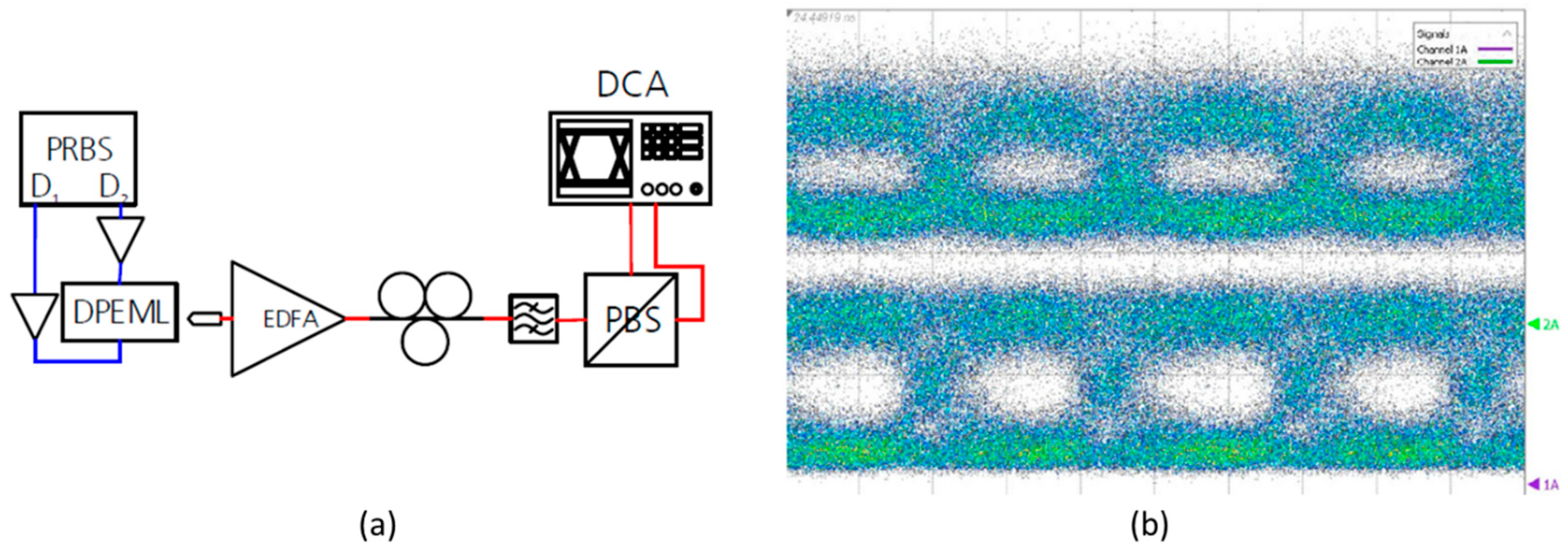
Figure 3b shows the response of the EAM to both polarizations as a function of the applied bias voltage. This plot shows that the EAM only responds to a TE-polarized optical signal, while leaving TM-polarized unchanged. Figure 3c shows the frequency response of the EAM for various applied voltages, illustrating a modulation bandwidth up to 12 GHz at present. Significantly higher bandwidths will be available in the future following dedicated design and processing optimization steps. The DC characterization of the fabricated DPEML PIC is done on a Stokes-calibrated measurement station. We use it to measure the Stokes vector of light exiting the device and its dependence on the two bias voltages. The measurement is done at a DFB bias of 130 mA, and the chip is placed on a TEC that is set to 20 °C. The fiber-coupled output power with unbiased EAMs is −23 dBm. This can be broken down to 3 dBm coming from the DFB, 2 dB loss per PR, 9 dB per EAM (including the epitaxial butt-joint interface), and 4 dB coupling loss to a tapered single mode fiber. A schematic of the measurement setup is shown in Figure 4a, and eye diagrams of both polarizations at 20 Gb/s are shown in Figure 4b. To verify the device’s data transmission capability, two electrical 20 Gbit/s non-return-to-zero (NRZ) signals are generated with a pseudo-random bit-sequence (PRBS) source. The signals are amplified with linear amplifiers to about 2 Vpp and launched onto the EAMs via high speed probes with a ground-signal-ground (GSG) configuration. To avoid back reflections, the probe has an AC-coupled 50 Ω resistor integrated. DC bias voltages are applied via bias-tees. The optical signal is amplified with an L-band Erbium-doped fiber amplifier (EDFA) and subsequently spectrally filtered. A polarization controller (PC) and a polarization beam splitter (PBS) are used on the receiver side together with two high-speed photodetectors and a digital communication analyzer (DCA) as a direct-detection receiver. The modulated optical power is −26.5 dBm. To make sure that the two recorded eye diagrams come from both EAMs, we turned off the electrical amplifier feeding one of the EAMs. As expected, only one of the two eyes closed. The bias voltages at the first- and second EAM are −4.6 and −4.7 V, respectively, with a laser current of 130 mA. The eye diagram stemming from the first EAM is more impaired due to some crosstalk that comes from the non-ideal 90° PR. The ER of this eye is 2.5 dB, the ER of the eye generated by the second EAM is 7 dB. The first eye’s ER is mostly limited by its DC fraction, which comes from light that was left un-rotated by the 90° PR. The SNR in both eyes is limited by the DPEML output power of −26.5 dBm. We believe that by improving the design in subsequent MPW shuttle runs, −6 dBm modulated output power and a reduction in crosstalk is achievable.
2.3. Balanced Waveguide Avalanche Photodetector Chip
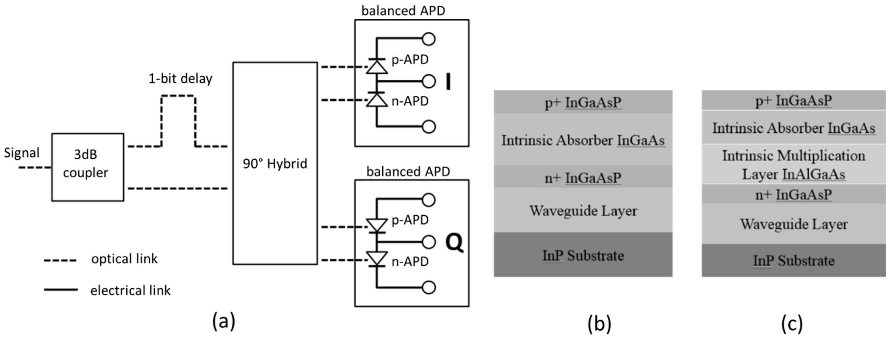
Higher-order modulation formats can efficiently increase channel capacity, but they typically require coherent receivers to detect the signal. Heterodyne coherent receivers require integration of an optical local oscillator, which increases the power consumption of the receiver. In contrast, homodyne coherent receivers (as shown on Figure 5a) include a 1-bit delay line, such that the previously received bit signal acts as the local-oscillator (LO) signal, thereby avoiding the need for a local oscillator. However, homodyne receivers suffer from a higher power penalty compared to heterodyne setups. This power-penalty problem can be overcome by using avalanche PDs (APDs) instead of pin-PDs, due to their higher sensitivity. In addition, when using balanced APDs instead of separate APDs, the differential input stage of the trans-impedance amplifier (TIA) can be eliminated to further reduce the power consumption. Thus, a homodyne receiver PIC with balanced APDs would be a step towards deployment of multilevel formats in datacenters.
Figure 5b shows a cross-section of the layer stack of the current photodiodes on the generic-foundry platform, showing that the absorbing region consists of intrinsic InGaAs. In order to introduce APDs into the generic-foundry process, a multiplication and charge layer consisting of InAlAs was added, to create a so-called separate charge absorption multiplication (SCAM) structure with a partially p-doped absorber region (see Figure 5c) [18,19]. This change in the layer stack of the photodiodes introduced almost no additional process steps to the existing generic-foundry process.
Figure 6a displays the measured dark current, photocurrent and resulting gain characteristics for a single waveguide APD. Up to a gain of M = 14, the reverse bias voltage remains below 16 V. At unity gain voltage of 8.5 V, the responsivity is higher than 0.60 A/W over the entire C-Band. The dark current is lower than 10 nA (Figure 6b). Additionally, the APD shows low polarization dependency where the PDL is below 0.5 dB. The f3dB bandwidth, as well as the linearity, was measured separately on chip level while applying different bias voltages U corresponding to different gains. The bandwidth (Figure 6c) is up to f3dB = 24 GHz for low gain at U = 12 V and decreases with increasing bias voltage. For a gain up to M = 5.5 at an operation voltage of U = 15 V, the resulting bandwidth is still f3dB = 20 GHz for both APDs of a balanced-detector configuration, being sufficient for 28 Gb/s. At a higher gain up to M = 14, a f3dB bandwidth of 17 GHz is obtained, resulting in a maximum gain-bandwidth-product of GBP = 238 GHz and a responsivity-bandwidth product of 147 A/W GHz. The linearity of the APD was determined by varying the input power and measuring the electrical ouput power at 20 GHz (Figure 6d). A good linear behavior for input powers in the range of −10 to 5 dBm was observed.
3. Building Blocks targeting Hybrid-Integration Applications
As explained in the introductory section, modules in datacenters will be relying more on hybrid integration to increase link- and channel capacity, while keeping size, power consumption, and cost low. The most relevant parameters for hybrid integration of different PICs into a compact module are: coupling loss, alignment tolerance, polarization dependent loss, and amount of back reflection. All these parameters are very much inter-related to each other by the way that the light is coupled from the InP PIC to the other PIC (here to be named, the interconnect PIC). Figure 7 shows four of the most common hybrid-integration approaches that are reported in the literature for datacenter- and optical-interconnect applications, which we have subdivided in two types: edge coupling, and surface coupling [20,21,22,23,24,25,26,27,28,29,30,31]. We have been developing three strategies to modify our generic-foundry-service process to enable efficient coupling of light in- and out of the InP PIC for these four hybrid-integration approaches. To achieve this, the following three adaptations are required: deeply-etched waveguide terminations (i.e., etched facets), second-order Bragg gratings to realize grating couplers, and vertical mirrors to steer the light to either the top- or the bottom surface of the PIC.
3.1. Etched Facets
The etched-facet building block that is being introduced into our generic-foundry process has already been employed successfully in the realization of a 4-channel scalable optical switch consisting of an InP-based PIC containing an array of SOAs flipped onto a Si/SiNx-based PIC containing the passive switch fabric [22,23]. Figure 8a shows the schematic implementation of the generic-foundry process, including the etched facets, and Figure 8b shows an SEM photograph of a waveguide with an etched-facet termination near a cleaved facet. Etched facets provide many benefits over cleaved-waveguide facets:
- They fix the I/O interface positions LInP of the PIC down to sub-micron accuracy, as opposed to cleaved facets, which practically have an accuracy Δxcleave,InP of around +/−10 µm (see Figure 8c)
- Reduction of back reflection at the facets by setting the angle α of the etched facet with respect to the waveguide (see Figure 8d)
- They set the desired output angle of the light (angle θ as shown in Figure 8d) independently from the angle α of the etched facet that affects the back reflection
- Possibility of applying optical coatings to the etched facets on-wafer and in a single coating process before cleaving or dicing
In the work reported in previous studies [22,23], we were able to achieve an SOA gain of 22–23 dB with the etched facets compared to a gain of 27–28 dB for SOAs with cleaved facets, resulting in an additional loss of ~2.5 dB introduced by the etched facets. In this case, the mode size of the waveguide at the etched facets was around 2.5 × 2.5 µm2, resulting in an increased loss and reflectivity (compared to that of a cleaved-facet SOA) due to the roughness from etching of the facet. When transferring this process to the generic foundry run, the etching process for the etched facets will be further optimized for lower roughness and lower etched-facet losses. In addition, the etched facets can also be etched on the diluted waveguides (see Figure 2a), where the mode size is much larger (~10 × 7 µm2), reducing the effect of the etched-facet roughness even further. The noise figure of the etched-facet SOAs reported in [22,23] was around 5–6 dB, and the length accuracy of the etched-facet SOAs was below ±0.5 µm (compared to ±3.5 µm for the cleaved SOAs).
Etched facets are advantageous for both edge-coupling concepts shown in Figure 7a,b, however it is important that the optical signal can propagate from one PIC to another (and, of course, also to optical fibers) without much beam divergence (i.e., large mode sizes) so that the light does not bounce off the pedestal that is introduced. As is shown in Figure 8a, a major advantage of our generic-foundry process is that it allows for the realization of SSCs with an MFD of 10 µm by 7 µm, resulting in a small beam divergence angle. This, in turn, allows for a rather large pedestal length (>10 µm) before a significant portion of the light hits the pedestal.
The etched facets are formed on-wafer (before cleaving) by a chemically-assisted ion-beam-etch (CAIBE) process. After structuring of the waveguides, a SiNx hard mask is deposited over the whole wafer. Then, the opening for the etching of the facet is defined by lithography followed by selective etching of the SiNx mask in a reactive-ion etcher. Afterwards, the photoresist was removed and a chlorine-assisted Ar IBE process was used to etch the InP down to ~9 µm. Then, an anti-reflection (AR) coating was applied on the sidewalls of the etched facets over the whole wafer using a SiNx layer deposited on a plasma-enhanced CVD.
3.2. Grating Couplers on InP Technology
Vertical coupling schemes are attractive because they enable deployment in free-space-optic applications, but also they enable on-wafer processing, characterization and testing, and vertical optical in/out coupling virtually at any site on the PIC chip without the need for prior chip cleaving and coating procedures. In silicon photonics, vertical grating couplers represent an established IO interface, however this is not yet the case for InP PICs, mainly due to the fact that compact grating couplers for coupling to an SMF are not possible because of the low index contrast waveguides. On the other hand, for hybrid integration employing surface-coupling approaches, there is no limitation on coupling to SMFs, and it is actually an advantage to have larger mode sizes with larger alignment tolerances. In addition, grating couplers can be designed to generate collimated beams with very low beam divergences, which means that the InP PIC and the interconnect PIC can be much farther apart without introducing a significant penalty to the coupling loss. The drawbacks of using grating couplers to couple light from the InP PIC to an interconnect PIC (as opposed to the other two coupling approaches described in this section) is that they are polarization- and wavelength dependent, which is an issue that PIC designers should take into account. An example of the utilization of InP grating couplers to realize a 2D beamsteering PIC is described in a previous study [31].
Figure 9 shows our implementation of grating couplers into the generic-foundry fabrication process for maximum coupling of the light through the bottom side of the PIC. This implementation does not require any change to the generic-foundry process, because such gratings can be implemented by using 2nd-order Bragg gratings (instead of 1st-order) in the Bragg Grating BB already available on the generic-foundry process. In the implementation shown in Figure 9, the light is coupled to the grating coupler, and the grating coupler starts emitting light to both the InP substrate and the InP top cladding in equal powers. On top of the InP cladding, a highly-reflective coating is added to redirect this light towards the bottom. If the top cladding has the correct thickness, then the light coming from the top cladding will interfere constructively with the light that was directly guided downwards. The coupling coefficient of the Bragg gratings currently offered on the foundry platform (for instance, on the first-order gratings on the DBR lasers) is around 80 cm−1, which results in a grating length of around 300 µm for 100% reflection. Considering the fact that the gratings on gratings couplers are second-order gratings (i.e., twice the first-order grating period) with the same coupling coefficient, this would result in a grating coupler length of 600 µm, and therefore, a mode size of 600 µm coming out of the grating coupler along the propagation direction. We believe that this length is too large for most practical free-space applications, and therefore in order to shorten the grating coupler length, we have increased the grating depth from 30 nm to 150 nm to increase the coupling coefficient of the gratings on the grating couplers (to reduce the grating coupler length from 600 µm to 200–300 µm).
3.3. Vertical Mirrors
An alternative surface-coupling approach is based on vertical mirrors, which are etched through the waveguides to divert the light upward or downward from the PIC. For the generic platform, we transfer the process from our commercial device that employs such vertical mirrors, which is the so-called horizontal-cavity surface-emitting laser (HCSEL) that consists of a conventional InP DFB laser with a vertical mirror etched at the end [32]. For this commercial device, we are able to couple 10 mW of output power at 100 mA of applied current at the top of the vertical mirror, where around 20 mW are expected in conventional DFB lasers with a cleaved facet. This 3 dB loss for the vertical-mirror etch is roughly the same as the loss for the etched facets described earlier, which is not surprising considering the fact that the etching process and tool (CAIBE) is the same except for the etching angle. Again, here it is expected that these losses caused by the roughness of the etching will not be so high for vertical mirrors etched into the diluted waveguide with the larger mode size. Figure 10a,b show our implementation of these vertical mirrors for the generic-foundry platform. Similar to the etched facets, the vertical mirrors are etched in a CAIBE tool by sloping the InP PIC with respect to the ion beam in the CAIBE. Simultaneously, another oppositely sloped 45° mirror is created, which reflects the laser light downwards into the substrate (Figure 10b). An additional advantage of these mirrors is that the optical coatings can be applied simultaneously over the whole wafer before cleaving. Vertical mirrors provide high efficiency and virtually wavelength and polarization-independent coupling, but it requires an additional processing step on our generic-foundry process. The fact that the generic-foundry process offers SSC BB with a large mode size (10 × 7 µm2) and small beam divergence, is advantageous for this coupling approach, as the light typically needs to travel some distance before reaching the SMF. A similar laser device employing vertical mirrors is the so-called lens-integrated surface emitting laser (LISEL), combining a laser, a vertical mirror, and an integrated collimating lens [33,34].
4. Conclusions
We have developed a generic foundry process for the realization of a wide variety of complex InP PICs. The generic foundry process provides PIC designers access to almost all devices available in InP technology, such as lasers, SOAs, high-speed photodiodes, balanced detectors, uniform-, sampled-, and superstructure gratings, spot-size converters, EAMs, phase modulators, and three types of passive waveguides serving as on-chip optical interconnects, as well as the basis for a wide range of passive-optical elements. We have highlighted two InP PICs that have been realized with this process. The first PIC was a fully-integrated dual-polarization electro-absorption-modulated laser, where we demonstrated operation at 20 Gb/s. The second PIC was a balanced detector composed of avalanche photodiodes for the detection of multi-level-format signals with a higher sensitivity than achievable with balanced detectors based on conventional pin photodiodes. Those APD structures can be seamlessly incorporated into HHI’s PIC platform just by modifying the epitaxial PD layer structure. The balanced APD showed a bandwidth of more than 17 GHz, and can be used for detecting multi-level optical signals at 28 Gb/s.
We have devised three concepts to facilitate the hybrid integration of InP PICs from our generic foundry platform to PICs from other technology platforms. These concepts require only minor modifications to the fabrication process, and all the other devices can still be realized with these modifications. The modifications that we are transferring are the following. First, introduction of waveguide terminations through etched facets instead of cleaved facets, which allows PIC designers to reduce the back reflections into the PIC and simultaneously control the angle of the output light. Second, addition of grating couplers to the PDK of the generic-foundry platform, which allows PIC designers to design grating coupler structures for coupling light out of the PIC through the surface. Third, introduction of vertical mirrors, which can alternatively be used to couple light out of the PIC through the top- or bottom surface of the PIC. We believe that these additional input/output interfacing options will prove useful in this era, where hybridization of PICs is becoming very important for datacenter- and optical-interconnect applications.
Author Contributions
Conceptualization, F.M.S., M.B., M.M., T.B., and P.R.; funding acquisition, N.G.; investigation, T.B.; methodology, T.G. and T.B.; project administration, F.M.S., M.M., and P.R.; resources, M.S.; supervision, M.M., P.R., and M.S.; writing—original draft, F.M.S.; writing—review and editing, M.B.
Funding
This research originated from the European Community´s Seventh Framework Programme FP7/2007-2013 under grant agreement ICT 257210 PARADIGM, and grant agreement NMP 228839 EuroPIC.
Conflicts of Interest
The authors declare no conflict of interest.
References
- Agrell, E.; Karlsson, M.; Chraplyvy, A.R.; Richardson, D.J.; Krummrich, P.M.; Winzer, P.; Roberts, K.; Fischer, J.K.; Savory, S.J.; Eggleton, B.J.; et al. Roadmap of optical communications. J. Opt. 2016, 18, 063002. [Google Scholar] [CrossRef] [Green Version]
- Urata, R.; Liu, H.; Zhou, X.; Vahdat, A. Datacenter interconnect and networking: From evolution to holistic revolution. In Proceedings of the 2017 IEEE Optical Fiber Communications Conference and Exhibition (OFC), Los Angeles, CA, USA, 19–23 March 2017. [Google Scholar]
- Thraskias, C.A.; Lallas, E.N.; Neumann, N.; Schares, L.; Offrein, B.J.; Henker, R.; Plettemeier, D.; Ellinger, F.; Leuthold, J.; Tomkos, I. Survey of photonic and plasmonic interconnect technologies for intra-datacenter and high-performance computing communications. IEEE Commun. Surv. Tutor. 2018, 20, 2758–2783. [Google Scholar] [CrossRef]
- Ghiasi, A. Large data centers interconnect bottlenecks. Opt. Express 2015, 23, 2085–2090. [Google Scholar] [CrossRef] [PubMed]
- Tatum, J.A.; Gazula, D.; Graham, L.A.; Guenter, J.K.; Johnson, R.H.; King, J.; Kocot, C.; Landry, G.D.; Lyubomirsky, I.; MacInnes, A.N.; et al. VCSEL-based interconnects for current and future data centers. J. Lightwave Technol. 2015, 33, 727–732. [Google Scholar] [CrossRef]
- Smit, M.; Leijtens, X.; Ambrosius, H.; Bente, E.; Van der Tol, J.; Smalbrugge, B.; de Vries, T.; Geluk, E.-J.; Bolk, J.; van Veldhoven, R.; et al. An introduction to InP-based generic integration technology. Semicond. Sci. Technol. 2014, 29, 083001. [Google Scholar] [CrossRef] [Green Version]
- Available online: www.jeppix.eu (accessed on 10 April 2019).
- Mourgias-Alexandris, G.; Vagionas, C.; Tsakyridis, A.; Maniotis, P.; Pleros, N. All-optical 10Gb/s ternary-CAM cell for routing look-up table applications. Opt. Express 2018, 26, 7555–7562. [Google Scholar] [CrossRef] [PubMed]
- Melati, D.; Alippi, A.; Melloni, A. Reconfigurable photonic integrated mode (de) multiplexer for SDM fiber transmission. Opt. Express 2016, 24, 12625–12634. [Google Scholar] [CrossRef] [PubMed]
- Carpintero, G.; Guzmán, R.C.; Lo, M.C.; Ali, M.; Zarzuelo, A.; Lamela, H.; García-Muñoz, L.E.; Segovia, D.; de Felipe, D.; Keil, N. Monolithic and Heterogeneous Microwave/Millimeter-wave Photonic Integrated Circuits. In Proceedings of the Conference on Lasers and Electro-Optics/Pacific Rim, Hong Kong, China, 29 July–3 August 2018; Optical Society of America: Miami, FL, USA, 2018. [Google Scholar]
- Sun, M.; Tan, S.; Guo, F.; Liu, S.; Kan, Q.; Lu, D.; Zhang, R.; Zhao, W.; Liang, S.; Wang, W.; et al. Integrated four-wavelength DFB diode laser array for continuous-wave THZ generation. IEEE Photonics J. 2016, 8, 1–8. [Google Scholar] [CrossRef]
- Ibrahim, S.K.; Farnan, M.; Karabacak, D.M. Design of a photonic integrated based optical interrogator. In Photonic Instrumentation Engineering IV; International Society for Optics and Photonics: San Diego, CA, USA, 2017; Volume 10110. [Google Scholar]
- Chang, M.P.; Blow, E.C.; Sun, J.J.; Lu, M.Z.; Prucnal, P.R. Integrated microwave photonic circuit for self-interference cancellation. IEEE Trans. Microwave Theory Techn. 2017, 65, 4493–4501. [Google Scholar] [CrossRef]
- Peng, H.T.; Nahmias, M.A.; de Lima, T.F.; Tait, A.N.; Shastri, B.J. Neuromorphic photonic integrated circuits. IEEE J. Sel. Top. Quantum Electron. 2018, 24, 1–15. [Google Scholar] [CrossRef]
- Liu, S.; Wang, H.; Sun, M.; Zhang, L.; Chen, W.; Lu, D.; Zhao, L.; Broeke, R.; Wang, W.; Ji, C. AWG-Based Monolithic 4 x 12GHz Multichannel Harmonically Mode-Locked Laser. IEEE Photonics Technol. Lett. 2016, 28, 241–244. [Google Scholar] [CrossRef]
- Soares, F.M.; Baier, M.; Gaertner, T.; Franke, D.; Moehrle, M.; Grote, N. Development of a versatile InP-Based photonic platform based on butt-joint integration. In Proceedings of the Conference on Lasers and Electro-Optics/Pacific Rim, Busan, Korea, 24–28 August 2015; Optical Society of America: San Diego, CA, USA, 2015. [Google Scholar]
- Baier, M.; Soares, F.M.; Moehrle, M.; Grote, N.; Schell, M. A New Approach to Designing Polarization Rotating Waveguides. Presented at the European Conference on Integrated Optics 2016, Warsaw, Poland, 18–20 May 2016. [Google Scholar]
- Campbell, J.C. Recent advances in avalanche photodiodes. J. Lightwave Technol. 2016, 34, 278–285. [Google Scholar] [CrossRef]
- Shimizu, S.; Shiba, K.; Nakata, T.; Kasahara, K.; Makita, K. 40 Gbit/s waveguide avalanche photodiode with p-type absorption layer and thin InAlAs multiplication layer. Electron. Lett. 2007, 43, 476–477. [Google Scholar] [CrossRef]
- Ohyama, T.; Doi, Y.; Kobayashi, W.; Kanazawa, S.; Takahata, K.; Kanda, A.; Kurosaki, T.; Tanaka, T.; Ohno, T.; Sanjoh, H.; et al. Compact hybrid integrated 100-Gb/s transmitter optical sub-assembly using optical butt-coupling between EADFB lasers and silica-based AWG multiplexer. J. Lightwave Technol. 2016, 34, 1038–1046. [Google Scholar] [CrossRef]
- Takahashi, H. High performance planar lightwave circuit devices for large capacity transmission. Opt. Express 2011, 19, B173–B180. [Google Scholar] [CrossRef] [PubMed]
- Schares, L.; Huynh, T.N.; Wood, M.G.; Budd, R.; Doany, F.; Kuchta, D.; Dupuis, N.; Lee, B.G.; Schow, C.L.; Moehrle, M.; et al. A Gain-Integrated Silicon Photonic Carrier with SOA-Array for Scalable Optical Switch Fabrics. In Optical Fiber Communication Conference; OSA Technical Digest (online); Optical Society of America: San Diego, CA, USA, 2016. [Google Scholar]
- Schares, L.; Budd, R.; Kuchta, D.; Doany, F.; Schow, C.; Möhrle, M.; Sigmund, A.; Rehbein, W. Etched-facet semiconductor optical amplifiers for gain-integrated photonic switch fabrics. In Proceedings of the 2015 IEEE European Conference on Optical Communication (ECOC), Valencia, CA, USA, 27 September–1 October 2015. [Google Scholar]
- Kleinert, M.; Zhang, Z.; de Felipe, D.; Zawadzki, C.; Novo, A.M.; Brinker, W.; Möhrle, M.; Keil, N. Recent progress in InP/polymer-based devices for telecom and data center applications. In Procedings of the SPIE 9365, Integrated Optics: Devices, Materials, and Technologies XIX; International Society for Optics and Photonics: San Diego, CA, USA, 2015; Volume 93650R. [Google Scholar]
- De Felipe, D.; Kleinert, M.; Zawadzki, C.; Polatynski, A.; Irmscher, G.; Brinker, W.; Moehrle, M.; Bach, H.-G.; Keil, N.; Schell, M. Recent developments in polymer-based photonic components for disruptive capacity upgrade in data centers. J. Lightwave Technol 2017, 35, 683–689. [Google Scholar] [CrossRef]
- Kurata, Y.; Nasu, Y.; Tamura, M.; Muramoto, Y.; Yokoyama, H.; Itoh, M. Fabrication of InP-PDs on silica-based PLC using heterogeneous integration technique. J. Lightwave Technol. 2014, 32, 2841–2848. [Google Scholar] [CrossRef]
- Hoose, T.; Billah, M.; Blaicher, M.; Marin, P.; Dietrich, P.I.; Hofmann, A.; Troppenz, U.; Moehrle, M.; Lindenmann, N.; Thiel, M.; et al. Multi-chip integration by photonic wire bonding: Connecting surface and edge emitting lasers to silicon chips. In Optical Fiber Communication Conference; Optical Society of America: California, CA, USA, 2016. [Google Scholar]
- Billah, M.R.; Blaicher, M.; Hoose, T.; Dietrich, P.I.; Marin-Palomo, P.; Lindenmann, N.; Nesic, A.; Hofmann, A.; Troppenz, U.; Moehrle, M.; et al. Hybrid integration of silicon photonics circuits and InP lasers by photonic wire bonding. Optica 2018, 5, 876–883. [Google Scholar] [CrossRef]
- De Dobbelaere, P.; Ayazi, A.; Chi, Y.; Dahl, A.; Denton, S.; Gloeckner, S.; Hon, K.-Y.; Hovey, S.; Liang, Y.; Mack, M.; et al. Packaging of silicon photonics systems. In Proceedings of the OFC 2014, San Francisco, CA, USA, 9–13 March 2014. [Google Scholar]
- Brusberg, L.; Neitz, M.; Pernthaler, D.; Weber, D.; Sirbu, B.; Herbst, C.; Frey, C.; Queisser, M.; Wöhrmann, M.; Manessis, D.; et al. Electro-optical circuit board with single-mode glass waveguide optical interconnects. In Optical Interconnects XVI; International Society for Optics and Photonics: San Diego, CA, USA, 2016; Volume 9753. [Google Scholar]
- Guo, W.; Binetti, P.R.; Althouse, C.; Mašanović, M.L.; Ambrosius, H.P.; Johansson, L.A.; Coldren, L.A. Two-dimensional optical beam steering with InP-based photonic integrated circuits. IEEE J. Sel. Top. Quantum Electron. 2013, 19, 6100212. [Google Scholar]
- Moehrle, M.; Kreissl, J.; Molzow, W.D.; Przyrembel, G.; Wagner, C.; Sigmund, A.; Grote, N. Ultra-low threshold 1490 nm surface-emitting BH-DFB laser diode with integrated monitor photodiode. In Proceedings of the 2010 22nd IEEE International Conference on Indium Phosphide and Related Materials (IPRM), Kagawa, Japan, 31 May–4 June 2010. [Google Scholar]
- Adachi, K.; Shinoda, K.; Fukamachi, T.; Shiota, T.; Kitatani, T.; Hosomi, K.; Matsuoka, Y.; Sugawara, T.; Aoki, M. A 1.3-µm lens-integrated horizontal-cavity surface-emitting laser with direct and highly efficient coupling to optical fibers. In Proceedings of the 2009 IEEE Conference on Optical Fiber Communication-Incudes Post Deadline Papers, Yinchuan, China, 10–11 August 2009. [Google Scholar]
- Adachi, K.; Suzuki, T.; Ohtoshi, T.; Nakahara, K.; Sagawa, M.; Nakanishi, A.; Naoe, K.; Tanaka, S. Facet-free surface-emitting 1.3-μm DFB laser. In Proceedings of the 2015 IEEE European Conference on Optical Communication (ECOC), Valencia, Spain, 27 September–1 October 2015. [Google Scholar]
Figure 1.
Schematic showing the epitaxial layers of the generic foundry process along the propagation direction, and the insets show cross-sections of the various waveguides. The purpose of the diluted waveguide structure is to implement I/O spot size converters with a much larger mode size (10 µm × 7 µm) than that of the other waveguides in the process (PD: photodetector; SOA: semiconductor optical amplifier; EAM: electro-absorption modulator; DFB: distributed feedback laser; SSC: spot-size converter).
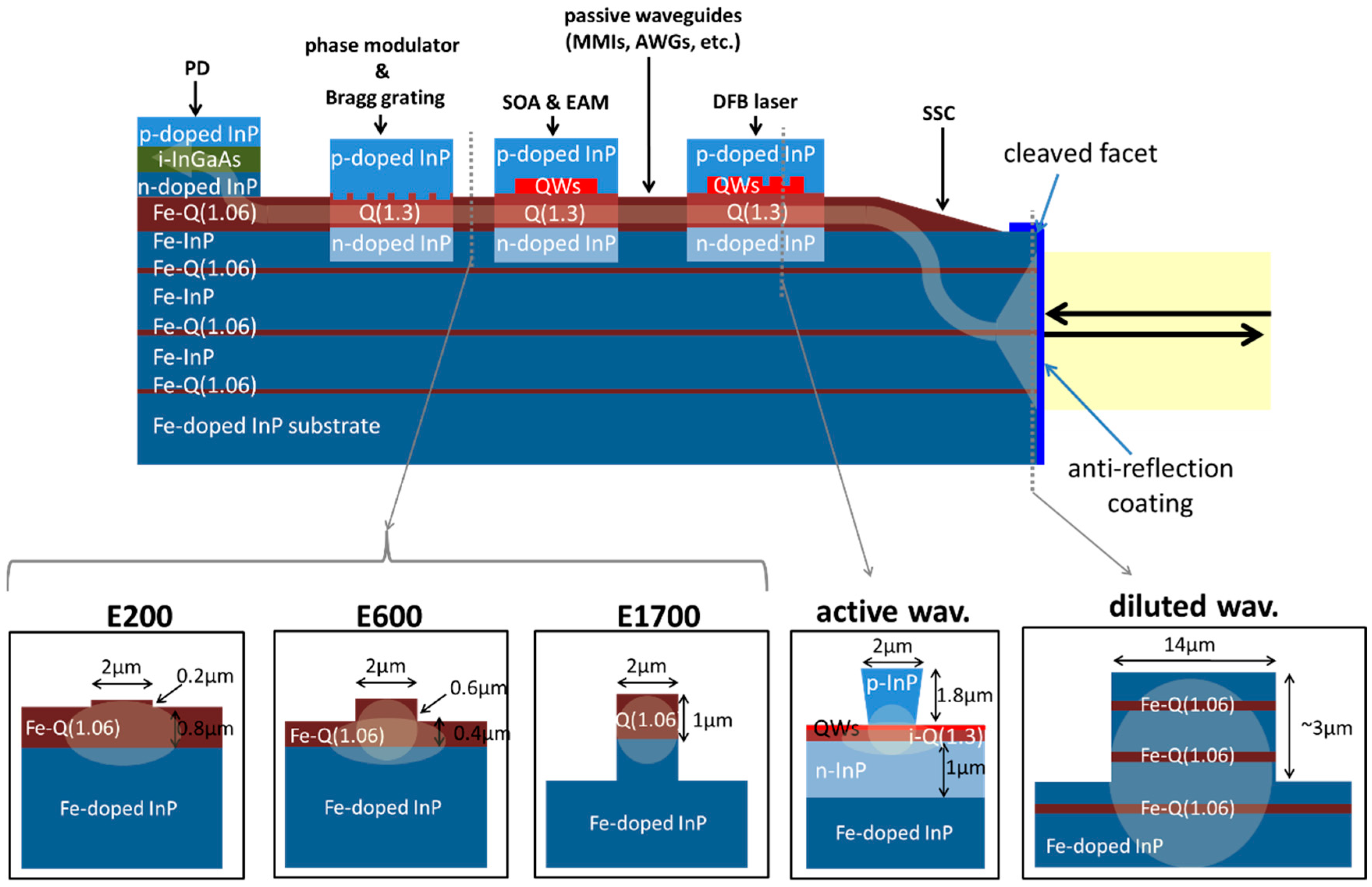
Figure 2.
Schematic of the spot-size converter seen in a bird´s view perspective with a plot of a simulation of the light propagation on the side (a), and a scanning-electron-microscope (SEM) photograph of the asymmetric waveguide used in the polarization rotator (b).
Figure 2.
Schematic of the spot-size converter seen in a bird´s view perspective with a plot of a simulation of the light propagation on the side (a), and a scanning-electron-microscope (SEM) photograph of the asymmetric waveguide used in the polarization rotator (b).

Figure 3.
Photograph of the fabricated dual-polarization electro-absorption-modulated laser (a), along with a plot showing the insertion loss of the EAM for bot polarizations (b), and a plot of the bandwidth of the EAM for various applied voltages (c).
Figure 3.
Photograph of the fabricated dual-polarization electro-absorption-modulated laser (a), along with a plot showing the insertion loss of the EAM for bot polarizations (b), and a plot of the bandwidth of the EAM for various applied voltages (c).

Figure 4.
Schematic of the measurement setup used to characterize the DPEML (a), and eye diagrams of the TE- and TM polarized signal from the DPEML at 20 Gb/s (b).
Figure 4.
Schematic of the measurement setup used to characterize the DPEML (a), and eye diagrams of the TE- and TM polarized signal from the DPEML at 20 Gb/s (b).

Figure 5.
Schematic of a homodyne receiver for multi-level format employing balanced avalanche photodetectors (a). Epitaxial layer stack of the waveguide photodiodes in the generic-foundry process (b), compared to the epitaxial layer stack of the waveguide avalanche photodiodes (c).
Figure 5.
Schematic of a homodyne receiver for multi-level format employing balanced avalanche photodetectors (a). Epitaxial layer stack of the waveguide photodiodes in the generic-foundry process (b), compared to the epitaxial layer stack of the waveguide avalanche photodiodes (c).

Figure 6.
Measurement results of the avalanche photodiodes: IV curve including the calculated gain (a), responsivity and PDL versus wavelength (b), frequency response for various applied voltages (c), and linearity for various input powers (d).
Figure 6.
Measurement results of the avalanche photodiodes: IV curve including the calculated gain (a), responsivity and PDL versus wavelength (b), frequency response for various applied voltages (c), and linearity for various input powers (d).

Figure 7.
Illustration of four of the most common approaches for hybrid integration of InP PICs with PICs from other technologies. (a): edge-coupling method through active alignment between the PICs (b) edge-coupling approach employing flip-chip alignment (c): surface-coupling approach with grating couplers (d): surface-coupling approach using 45° vertical mirrors.
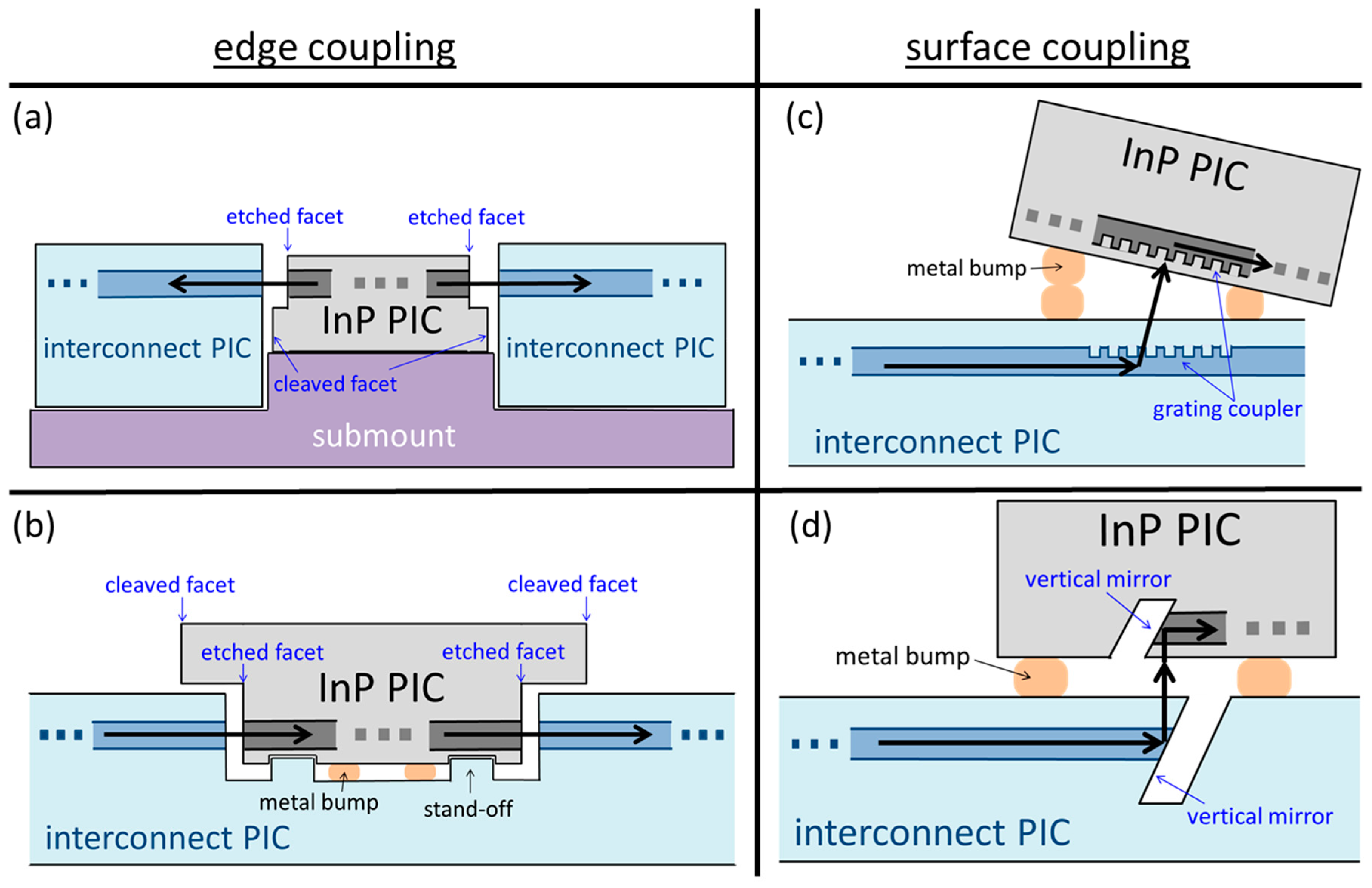
Figure 8.
Schematic showing the implementation of etched facets on the generic-foundry process (a). SEM photograph of a diluted waveguide with an etched facet near a cleaved facet (b), a top view schematic of the coupling between an InP PIC and an interconnect PIC (c), and an illustration of the parameters involved in defining the required etched-facet properties (d).

Figure 9.
Schematic showing an implementation of grating couplers on the generic-foundry-service process.
Figure 9.
Schematic showing an implementation of grating couplers on the generic-foundry-service process.

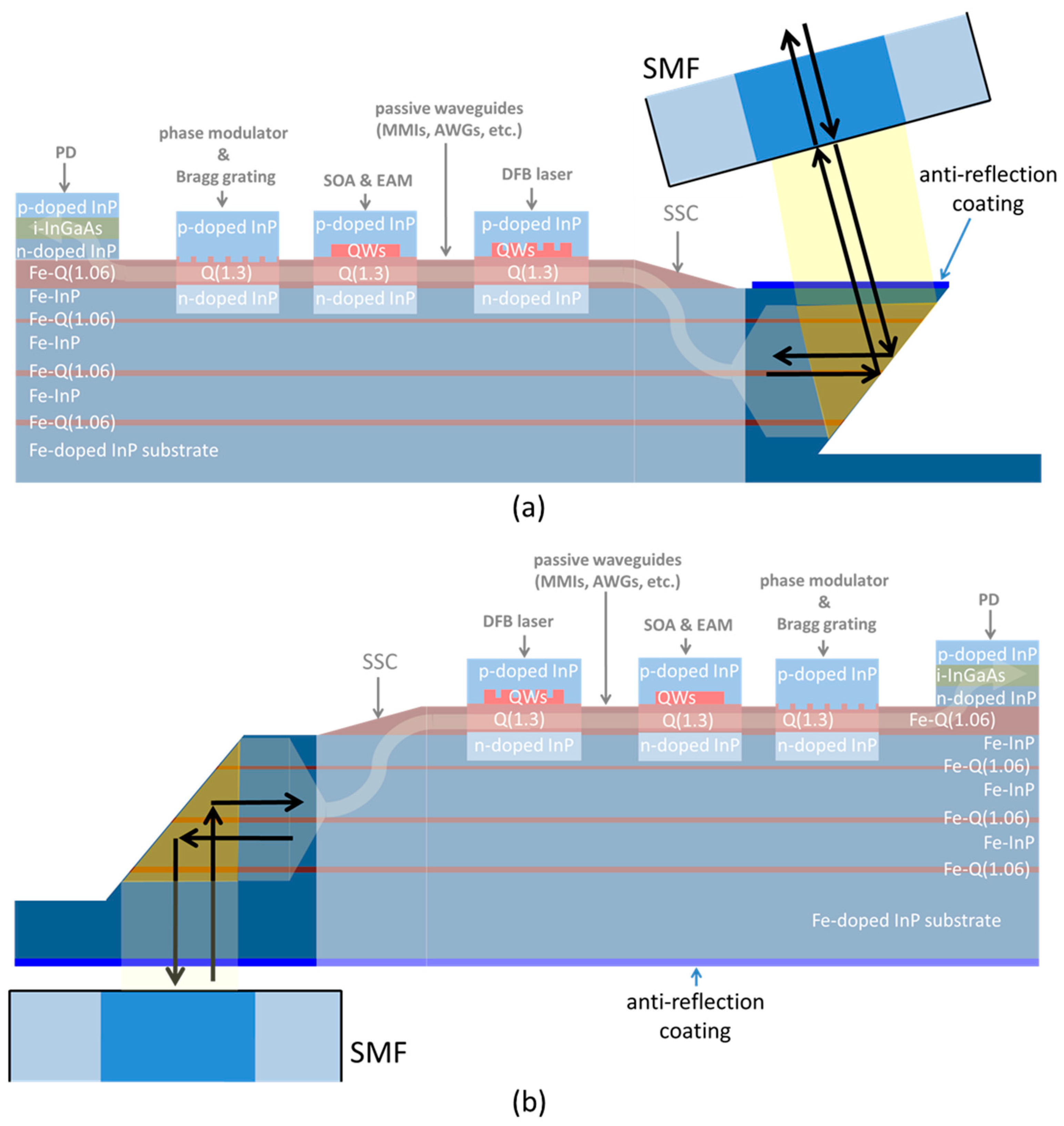
Figure 10.
Schematic showing the implementation of vertical mirrors on the generic-foundry-service process for coupling light upward (a), and downward (b).
Figure 10.
Schematic showing the implementation of vertical mirrors on the generic-foundry-service process for coupling light upward (a), and downward (b).
© 2019 by the authors. Licensee MDPI, Basel, Switzerland. This article is an open access article distributed under the terms and conditions of the Creative Commons Attribution (CC BY) license (http://creativecommons.org/licenses/by/4.0/).
Share and Cite
MDPI and ACS Style
Soares, F.M.; Baier, M.; Gaertner, T.; Grote, N.; Moehrle, M.; Beckerwerth, T.; Runge, P.; Schell, M. InP-Based Foundry PICs for Optical Interconnects. Appl. Sci. 2019, 9, 1588. https://doi.org/10.3390/app9081588
AMA Style
Soares FM, Baier M, Gaertner T, Grote N, Moehrle M, Beckerwerth T, Runge P, Schell M. InP-Based Foundry PICs for Optical Interconnects. Applied Sciences. 2019; 9(8):1588. https://doi.org/10.3390/app9081588
Chicago/Turabian StyleSoares, Francisco M., Moritz Baier, Tom Gaertner, Norbert Grote, Martin Moehrle, Tobias Beckerwerth, Patrick Runge, and Martin Schell. 2019. "InP-Based Foundry PICs for Optical Interconnects" Applied Sciences 9, no. 8: 1588. https://doi.org/10.3390/app9081588
Note that from the first issue of 2016, this journal uses article numbers instead of page numbers. See further details here.