High-Sensitive TM Modes in Photonic Crystal Nanobeam Cavity with Horizontal Air Gap for Refractive Index Sensing


Department of Optical Engineering, Kongju National University, Cheonan 31080, Korea
*
Author to whom correspondence should be addressed.
Appl. Sci. 2019, 9(5), 967; https://doi.org/10.3390/app9050967
Submission received: 26 February 2019
/
Accepted: 4 March 2019
/
Published: 7 March 2019
(This article belongs to the Special Issue Novel Advances in Optical Micro- and Nano-Cavities)
Abstract
:We propose a new type of refractive index sensing based on the transverse magnetic (TM) modes in the photonic crystal (PhC) nanobeam (NB) cavity with a horizontal air gap. The electric field of the resonant TM mode is strongly confined within the horizontal air gap present at the PhC NB cavity. In order to increase the quality (Q) factor and the sensitivity (S) of the refractive index change in the air simultaneously, the cavity structure is fully optimized. Because of the trade-off between the Q-factor and S of the TM mode in the PhC NB cavity with an air gap, there is an optimal thickness of the air gap in the dielectric slot. From the numerical simulation results, S can exceed 1000 nm/RIU with Q > 40,000. When the dielectric slot becomes thin, S could be higher than 1200 nm/RIU. For practical applications, we suggest an Si-based PhC NB cavity with a horizontal SiO2 slot structure which can also provide high S with a high Q-factor after a very fine selective wet etching process. This new type of TM resonant mode in the PhC NB cavity can be an ideal platform for compact sensors in photonic integrated circuits for TM waveguide systems.
1. Introduction
Photonic crystals (PhCs) have been widely studied for their ability to prohibit light propagation due to their photonic bandgap (PBG) [1,2]. In particular, PhC cavity structures have attracted many researchers due to their small modal volume (V) and high quality (Q) factor with help of the rapid development of nanotechnology processes such as lithography and dry etching [3,4,5]. One of the possible applications of PhC cavity structures is optical sensing based on wavelength shift due to environmental changes such as pH changes, chemical changes, and strain changes [6,7,8].
Recently, PhC nanobeam (NB) structures have been proposed as new types of optical integrated circuits because of structural simplicity to achieve an ultrahigh Q/V ratio and direct coupling to optical waveguides [9,10,11]. Furthermore, PhC NB cavity structures are ideally suitable for ultrasensitive optical sensing with an extremely small footprint because of the deterministic wavelength-scale design [12,13]. Moreover, nanometer-wide air gap geometry surrounded by a high-index region was proposed to enhance and confine the light [14]. As the electric field could be tightly concentrated in the air void by large discontinuity at the high-index-contrast interfaces, the Q/V ratio and optical sensitivity of the resonant mode in PhC cavity structures with an air gap could increase dramatically [15,16]. However, by introducing the air gap geometry in the PhC cavity, the Q-factor decreased due to a high scattering loss. Consequently, the deterministic PhC NB cavity with an air gap was proposed to achieve a high coupling efficiency to the waveguide with a high Q factor [17,18]. The Q-factor of the resonant cavity mode in PhC NB structures could be increased easily by adding more air holes outside the cavity region to reduce the loss along the waveguide.
It was also reported that the light could be localized strongly with low index materials in a horizontal slot region [19]. In particular, the scattering loss in the horizontal slot region is smaller than that in the vertical slot due to the smooth interface formed by the simple selective wet etching or oxidation process. Additionally, the horizontal air gap can be made ultrathin by controlling the deposition process, which can enhance the light−matter interaction [20,21]. However, the light localization in the horizontal slot is found in the transverse magnetic (TM) mode among the guided modes in the slab where there is no PBG [19,20]. In contrast, the PhC NB structure can have the PBG in both transverse electric (TE) and TM modes [22]. There are several reports related to the horizontally slotted PhC NB cavity; however, there was no systematical investigation of PhC NB cavities for gas sensing [23,24]. In this paper, we numerically investigate the TM mode in a PhC NB cavity with a horizontal air gap from the origin of the PBG to the whole transmission response by the three-dimensional (3-D) plane wave expansion method and the finite-difference time-domain (FDTD) method. Because of the intrinsic trade-off between the Q-factor and the sensitivity of the TM mode in the PhC NB cavity with an air gap, there is an optimal thickness of the air gap in the dielectric slot. The optimized PhC NB cavity is ultrasensitive to a refractive index change of approximately 1020 nm/RIU with Q > 40,000. When the dielectric slot becomes thin, the sensitivity can exceed 1200 nm/RIU. For practical applications, we suggest and Si-based PhC NB cavity with a horizontal SiO2 slot structure. After the very fine selective etching of SiO2, the PhC NB cavity with the remaining SiO2 can be mechanically stable and provide high sensitivity with a high Q-factor. The PhC NB cavity with the horizontal air gap can be considered promising for label-free compact optical sensors in photonic integrated circuits for TM waveguide systems.
2. Methods and Materials
2.1. Photonic Band Structure of TM Modes in PhC NB Structure with a Horizontal Air Gap
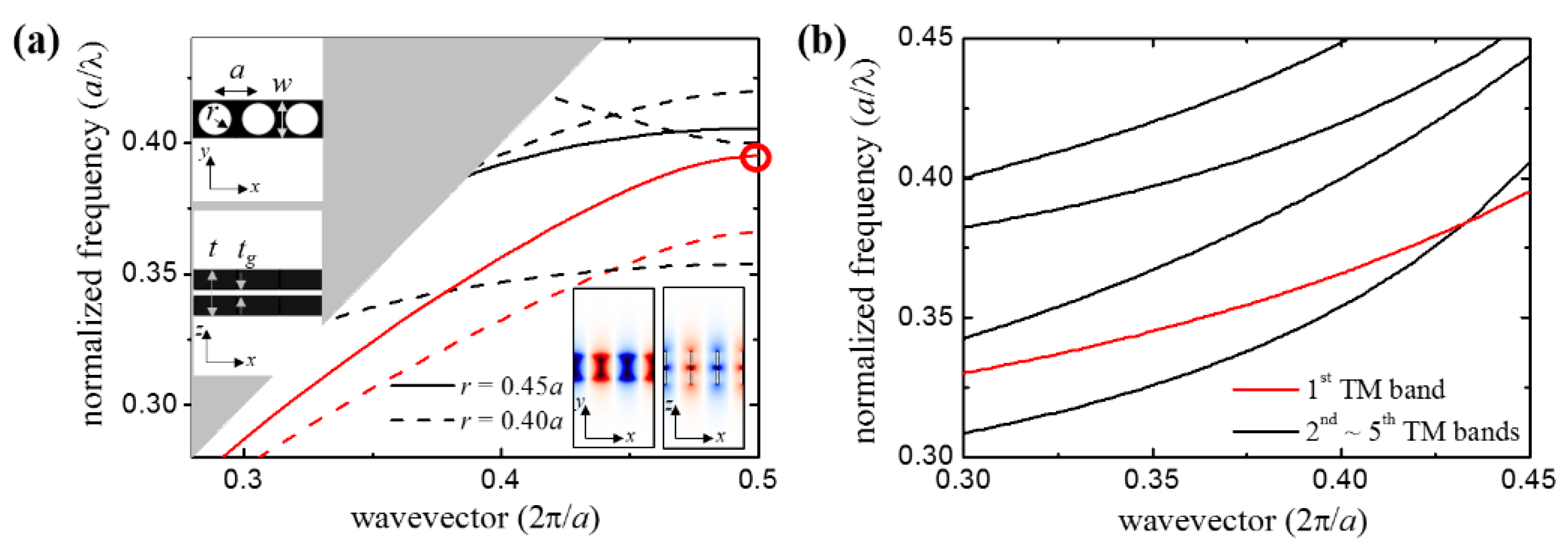
Firstly, the photonic band diagram of the TM mode in the PhC NB structure with a horizontal air gap was numerically calculated using the plane wave expansion method [25]. In this study, a free-standing silicon (n(Si) = 3.4) waveguide was used because it exhibited no optical absorption and a high refractive index of Si at the telecommunication wavelength, 1.55 μm. The upper inset of Figure 1a shows the schematic of the PhC NB structure in which the circular holes were perforated periodically. To carry out the simulation, the width (w), thickness (t), and air gap (tg) of the Si waveguide were set as 0.95a, 1.2a, and 0.15a, respectively, where a is the lattice constant of the air holes. Figure 1a shows the photonic band diagram of the TM modes with r/a = 0.45 (the solid lines) and r/a = 0.40 (the dashed lines). The solid and dashed red lines indicate the first TM photonic bands at r/a = 0.45 and r/a = 0.40, respectively. As shown in the lower inset of Figure 1a, the first TM mode corresponds to the air gap mode because of the strongly localized electric field distribution at the air region. It can be observed that the normalized frequency of the first TM mode with r/a = 0.45 at the band edge (wavevector, k = π/a) is in the PBG of the TM mode with r/a = 0.40.
To confine the light in the cavity of PhCs, the resonant frequency of the cavity mode should lie inside the frequency range of the PBG. Figure 1b shows the frequencies of the band edge modes as a function of r/a. It can be observed that the frequencies of the TM band edge modes decrease as r/a increases. Therefore, to confine the light using the air gap mode, the surrounded air hole should be smaller than the air hole in the cavity region. In this paper, we used r/a = 0.45 at the center of the PhC NB cavity which was surrounded by air holes with r/a = 0.405 as the PBG mirror.
2.2. Optimization of Waveguide Geometry of PhC NB Cavity Structure with a Horizontal Air Gap
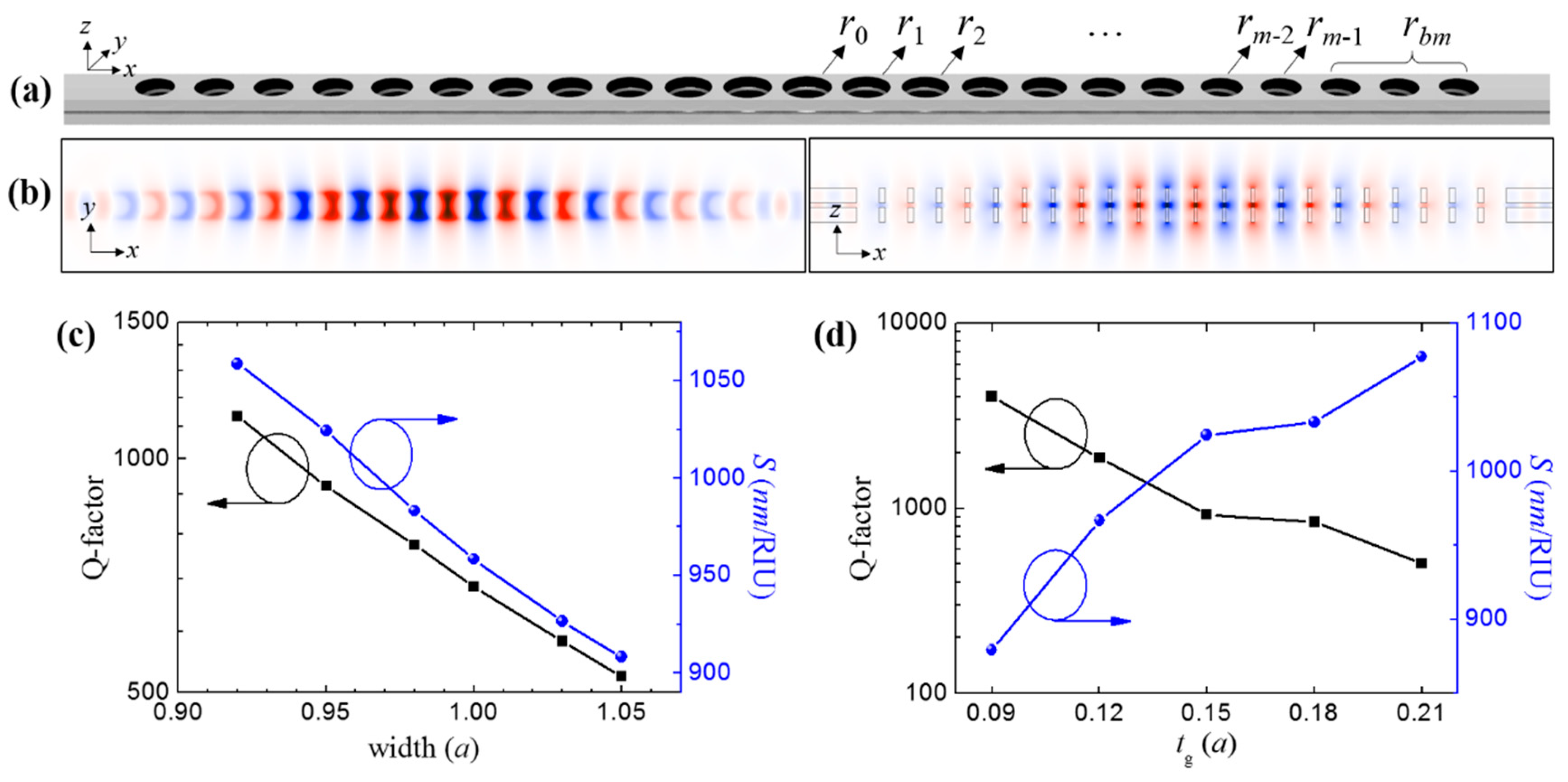
The PhC NB cavity with the horizontal air gap was designed for optimal refractive index sensing using the FDTD method. Figure 2a shows the schematics of the proposed PhC NB cavity structure with a horizontal air gap. According to the previous photonic band calculation, the radius of the air hole, r0, at the center is set as 0.45a. The radius of the surrounded air hole is gradually reduced to rbm, which represents the air holes acting as a PBG mirror for the cavity mode. In this simulation, three air holes with radius rbm are used as a PBG mirror at each waveguide end. It is worth noting that in order to achieve a high Q-factor and sensitivity simultaneously, the radius of the air holes is reduced in a quadratic manner because the dispersion curve of the air gap mode is parabolic, as discussed later in detail [9]. The radius of the i-th air hole from the center is set as:
where m is the total number of gradually reduced air holes. Here, m = 9 and the variation in the size of air holes, Δr (=r0 − rbm), is set as 0.10 r0. All other structural parameters are the same as the previous band diagram calculation. Figure 2b shows the cut-views of the electric field distribution, Ez, of the air gap cavity mode along the center plane of the air gap when the width and thickness of the air gap are w = 0.95a and tg = 0.15a, respectively. According to the x–z cut-view, the electric field of the cavity mode is strongly confined in the air gap region, which makes very sensitized to the refractive index change to the environment.
ri = r0 – i2Δr/m2
For practical applications of optical sensing, it is necessary to achieve not only high sensitivity but also a high Q-factor. In the first optimization step, we investigated the effect of the width of the Si waveguide on both sensitivity and Q-factor. The sensitivity, S, was defined as follows:
where Δλres is the peak wavelength shift of the cavity mode due to the refractive index change of the environment, Δn. Here, we set the range of the refractive index change as 1.000 to 1.001 considering the gas sensing. Figure 2c shows the Q-factor and S as functions of the width of the Si waveguide. As the width of the waveguide increases, both the Q-factor and S decrease. The reduction of S and the Q-factor at greater widths is caused by an increase in the electric field in the dielectrics and an increase in waveguide loss, respectively. In contrast, as the thickness of the air gap increases, the Q-factor decreases but S increases. The enhancement of S and reduction of the Q-factor is caused by the increase in the air portion and the weak PBG effect, respectively. So, there is a trade-off in order to obtain both a high Q-factor and S. Here, we set t and tg as 1.2a and 0.15a, respectively.
S = Δλres/Δn
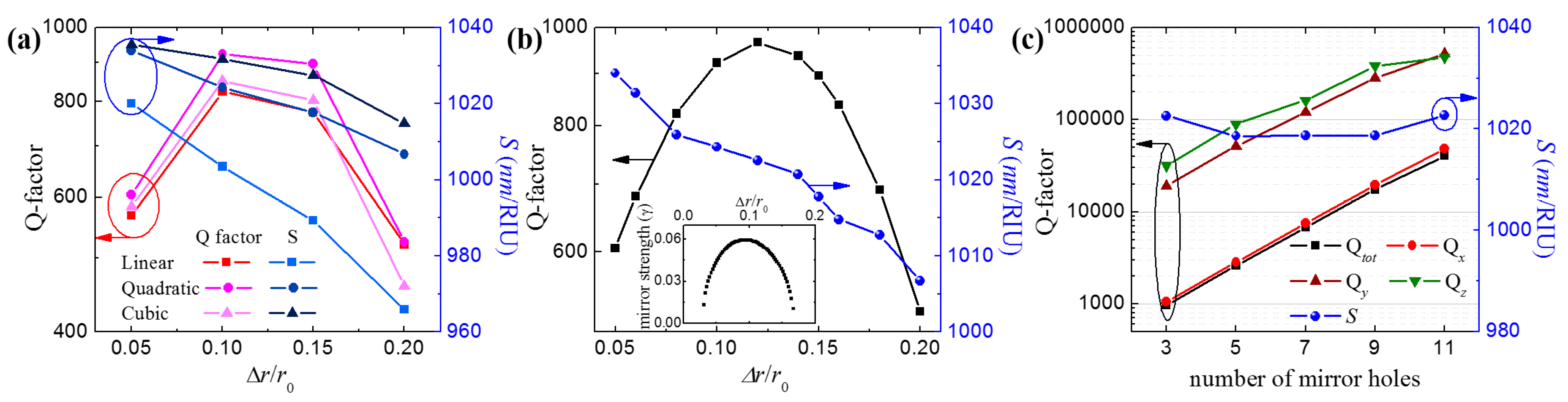
In the second optimization step for a high Q-factor and S, we investigated the modulation function to reduce air holes from the center to the mirror holes in the PhC NB cavity. Figure 3a shows the Q-factor and S of the air gap cavity mode as a function of the variation of air holes. Here, we employed three different modulation functions; linear, quadratic, and cubic functions. The cavity mode of cubic modulation has a slightly higher S than that of quadratic modulation because the air hole near the center is slightly larger. However, the Q-factor of the cavity mode of quadratic modulation is 8% higher than that of cubic modulation due to a relatively strong PBG effect. Next, we optimized the variation of the air hole to achieve the maximal Q-factor. Figure 3b shows the Q-factor and S as functions of the variation in the size of air holes. Q achieved a maximum value of approximately 970 at Δr = 0.12r0, which is limited by the waveguide loss. To understand the optimal condition of waveguide loss, mirror strength (γ), as shown in the inset graph of Figure 3b, was calculated using the following equation [10,18]:
where ω1 and ω2 are the frequencies of the first band edge mode and third band edge mode, respectively, in the PhC NB structure with rbm obtained from Figure 1b. ω0 and ωres are the mid-gap frequency (= (ω2 + ω1)/2) and resonant frequency of the air gap cavity mode, respectively, calculated using the FDTD method. According to the mirror strength, the strongest PBG effect is observed around Δr/r0 = 0.1, and therefore, the waveguide loss is minimized. Even though the PBG effect is maximized, the Q-factor is less than 1000, which is not enough for gas sensing. Fortunately, the PBG effect can be strengthened by simply adding mirror air holes. To examine this, we investigated the changes in the Q-factor and S as the number of mirror holes increased. For the quantitative analysis and maximization of the Q-factor and S of the air gap cavity mode, we investigated the loss mechanism. As mentioned earlier, the material loss was ignored because Si is a lossless material at a wavelength of 1.55 μm. Therefore, the total loss, αtot, is caused by the leakage of light, which can be expressed as αtot = αx + αy + αz where αi indicates the optical loss along i-axis (the axis direction is shown in Figure 2a). If this equation is re-expressed in terms of the Q-factor, then
From the simulation, all the Q-factors were obtained by carrying out Poynting flux calculations. Figure 3c shows that adding more mirror holes reduces the waveguide loss. From these results, we could simultaneously obtain a very high sensitivity (~1020) and a high Q-factor (>40,000) from the TM cavity mode in an optimized PhC NB with an air gap.
γ = [(ω2 − ω1)2/(ω2 + ω1)2 – (ωres – ω0)2/ ω02]1/2
1/Qtot = 1/Qx + 1/Qy + 1/Qz
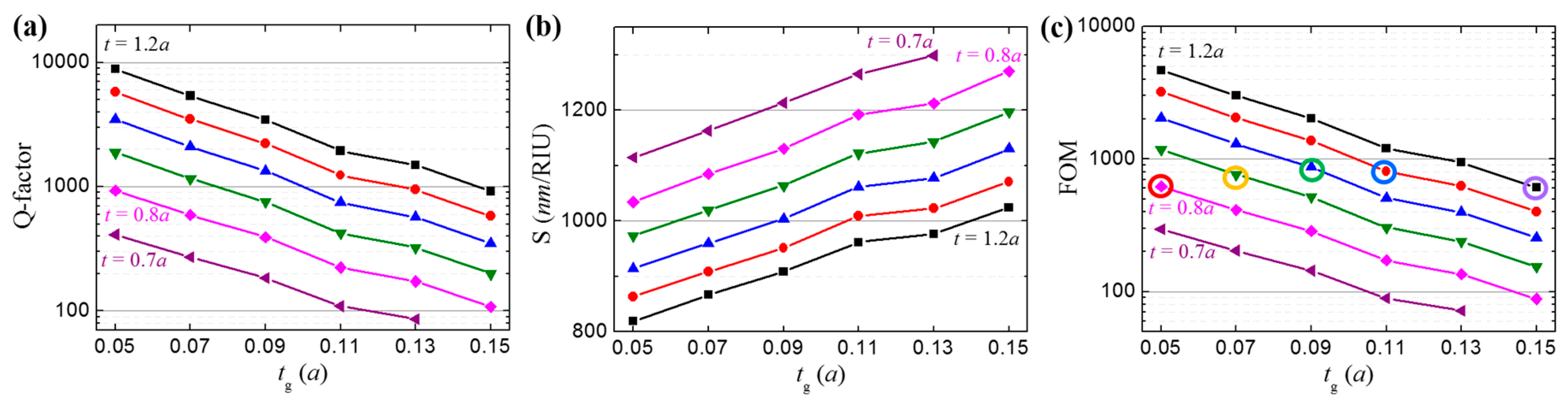
As shown in Figure 2d, there is trade-off between the Q-factor and S in the air gap cavity mode in the PhC NB cavity with the horizontal air gap, because a thick horizontal air gap increases the optical sensitivity but decreases the light confinement. Therefore, there is an optimal condition for both a high Q-factor and sensitivity. For the practical design of the optical sensor, we numerically investigated the Q-factor and S of the air gap cavity mode with various thicknesses of the Si waveguide and horizontal air gaps. Figure 4a shows Q-factors of the air gap cavity mode as functions of the thickness of the air gap with various thicknesses of the Si waveguide. According to these results, the Q-factor increases when the horizontal air gap becomes thin and the Si waveguide becomes thick, which is caused by a strong PBG effect from the high index contrast. However, the value of S of the air gap cavity mode shows exactly the opposite behavior compared with the Q-factor owing to the increase in the air portion (See Figure 4b). In particular, S can exceed 1200 nm/RIU when the air portion increases even though the Q-factor becomes low. For the evaluation of the optical sensing performance, the figure of merit (FOM) was defined as follows [26]:
where λres is the resonant wavelength. Figure 4c shows the FOM of the air gap cavity mode as a function of thickness of the air gap with various thicknesses of the Si waveguide. Because the Q-factor increases exponentially with decreasing tg, the FOM shows a similar behavior to that of the Q-factor. For the best performance of the optical sensor, the Q-factor should be balanced with S. Therefore, the PhC NB cavity structures with different thicknesses of the Si waveguide have different optimal thicknesses of the air gap, as marked with circles in Figure 4c, which have similar a Q-factor (~1000) and S (~1000 nm/RIU), simultaneously. It is worth noting that by simply increasing the number of mirror holes, the Q-factor could be exponentially increased; therefore, the optimal thickness of the air gap is also changed.
FOM = S · Q/λres
3. Discussion
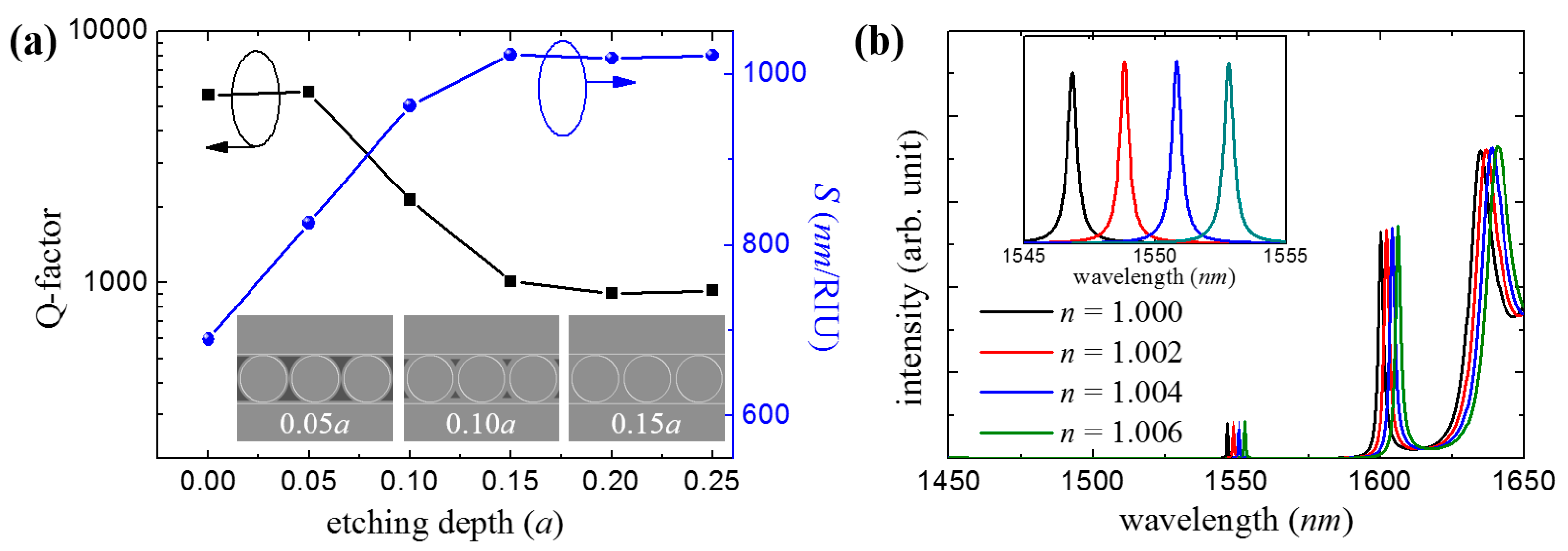
In practical applications, it may not be easy to fabricate the air gap using a selective wet etching process due to the capillary-force action [20,21]. Therefore, a few parts of the sacrificial layer should be carefully left to avoid the collapse of the dielectric slots by controlling the etching conditions [27]. We studied the effect of the remaining sacrificial layer on optical loss and S when the horizontal etching depth was varied. In the simulation, we used the optimized PhC NB cavity with three mirror holes as shown in Figure 3b. Here, we assume that the etching speed from the sidewall is isotropic. The inset of Figure 5a shows the horizontal cut-view of the sacrificial layer (SiO2) at the center of the PhC NB cavity structure. The black and gray areas indicate the remaining SiO2 layer and the air, respectively. The white lines indicate the outline of the Si dielectric slot. When the etching depth exceeds 0.15a, SiO2 at the cavity region is completely removed. Therefore, from the simulation results, both the Q-factor and S are almost constant when the etching depth is over 0.15a. However, if the etching depth is less than 0.15a, S decreases suddenly, which is caused by the reduction of the electric field in the environment. When the air switches to SiO2, the mirror strength increases due to the red-shift of the TM band edge modes. Consequently, the waveguide loss decreases and the Q-factor increases. In consideration of mechanical stability and easy fabrication, the PhC NB cavity with a SiO2 layer after fine selective etching (depth < 0.05a) is a good candidate for practical applications of gas sensing because of the high Q (> 5000) and S (> 800).
Finally, we studied the transmission spectra in an Si/air/Si TM waveguide system with the optimized air-slot cavity structure. In the simulation, the total number of mirror holes was set as five in order to save computational time. Figure 5b shows the transmission spectra of the PhC NB cavity with different refractive indices of the environment. The sharp peak observed near 1550 nm corresponds to the TM air gap cavity mode with a = 585 nm. Below 1550 nm, the transmitted intensity is zero owing to the PBG effect. However, modulated peaks are observed beyond 1600 nm. These are the higher order TM air gap cavity modes in the PhC NB cavity. According to the magnified spectra shown in the inset of Figure 5b, the Q-factor and S of the air gap cavity mode are 4000 and 1000 nm/RIU, respectively. We believe that this high value of Q and ultrasensitive PhC NB TM waveguide system with very small dimensions (~14 × 0.5 × 0.8 μm3) can be considered promising for compact optical sensors in photonic integrated circuits composed of TM waveguide structures with low index slots filled with dielectric gain media or non-linear materials [19]. In particular, this proposed system is based on the TM guided mode, and therefore can serve as an excellent surface plasmon coupling system with a certain resonance wavelength.
4. Conclusions
We numerically investigated a new type of ultrahigh sensitive optical sensor based on the TM mode in a PhC NB cavity structure with a horizontal air gap. The electric field of the resonant TM mode is strongly confined in the horizontal air gap at the center of the dielectric slots of the PhC NB cavity. There is an optimal thickness of the air gap in the dielectric slot because of the trade-off between the Q-factor and S of the TM mode in the PhC NB cavity with an air gap. By optimizing the PhC NB cavity, the maximum sensitivity achieved was over 1000 nm/RIU with Q > 40,000. When the dielectric slot becomes thin, the sensitivity could be further increased to over 1200 nm/RIU. For practical applications, a Si-based PhC NB cavity with a horizontal SiO2 slot structure was proposed, which was found to be mechanically stable after the fine selective etching of SiO2 and maintained high sensitivity with a high Q-factor. This new type of TM resonant mode in PhC NB cavity could be an ideal platform for compact sensors in photonic integrated circuits for TM waveguide systems.
Author Contributions
J.-K.Y.—Supervision, Project administration, Writing—original draft, Writing—Review and Editing, Methodology; C.-Y.K.— Investigation; M.L.—Investigation.
Funding
This research was supported by a research grant from the Kongju National University in 2017.
Conflicts of Interest
The authors declare no conflict of interest.
References
- Yablonovitch, E. Inhibited spontaneous emission in solid-state physics and electronics. Phys. Rev. Lett. 1987, 58, 2059–2062. [Google Scholar] [CrossRef] [PubMed]
- John, S. Strong localization of photons in certain disordered dielectric lattices. Phys. Rev. Lett. 1987, 58, 2486–2489. [Google Scholar] [CrossRef] [PubMed]
- Painter, O.; Lee, R.K.; Yariv, A.; Scherer, A.; O’Brien, J.D.; Dapkus, P.D.; Kim, I. Two-dimensional photonic band-gap defect mode laser. Science 1999, 284, 1819–1824. [Google Scholar] [CrossRef] [PubMed]
- Park, H.G.; Kim, S.H.; Kwon, S.H.; Ju, Y.G.; Yang, J.K.; Baek, J.H.; Kim, S.B.; Lee, Y.H. Electrically driven single-cell photonic crystal laser. Science 2004, 305, 1444–1447. [Google Scholar] [CrossRef] [PubMed]
- Akahane, Y.; Asano, T.; Song, B.S.; Noda, S. High-Q photonic nanocavity in a two-dimensional photonic crystal. Nature 2003, 425, 944–947. [Google Scholar] [CrossRef] [PubMed]
- Lee, K.; Asher, S.A. Photonic crystal chemical sensors: pH and ionic strength. J. Am. Chem. Soc. 2001, 122, 9534–9537. [Google Scholar] [CrossRef]
- Loncar, M.; Scherer, A.; Qiu, Y. Photonic crystal laser sources for chemical detection. Appl. Phys. Lett. 2003, 82, 4648–4650. [Google Scholar] [CrossRef]
- Choi, J.-H.; No, Y.-S.; So, J.-P.; Lee, J.M.; Kim, K.-H.; Hwang, M.-S.; Kwon, S.-H.; Park, H.-G. A high-resolution strain-gauge nanolaser. Nat. Commun. 2016, 7, 11569. [Google Scholar] [CrossRef] [PubMed] [Green Version]
- Notomi, M.; Kuramochi, E.; Taniyama, H. Ultrahigh-Q nanocavity with 1D photonic gap. Opt. Express 2008, 16, 11095. [Google Scholar] [CrossRef] [PubMed]
- Quan, Q.; Deotare, P.B.; Loncar, M. Photonic crystal nanobeam cavity strongly coupled to the feeding waveguide. Appl. Phys. Lett. 2010, 96, 203102. [Google Scholar] [CrossRef] [Green Version]
- Jeong, K.Y.; No, Y.S.; Hwang, Y.; Kim, K.S.; Seo, M.K.; Park, H.G.; Lee, Y.H. Electrically driven nanobeam laser. Nat. Commun. 2013, 4, 2822. [Google Scholar] [CrossRef]
- Quan, Q.; Burgess, I.B.; Tang, S.K.Y.; Floyd, D.L.; Loncar, M. High-Q, low index-contrast polymeric photonic crystal nanobeam cavities. Opt. Express 2011, 19, 22191–22197. [Google Scholar] [CrossRef] [PubMed]
- Kim, S.; Kim, H.-M.; Lee, Y.-H. Single nanobeam optical sensor with a high Q-factor and high sensitivity. Opt. Lett. 2015, 40, 5351. [Google Scholar] [CrossRef] [PubMed]
- Almeida, V.R.; Xu, Q.; Barrios, C.A.; Lipson, M. Guiding and confining light in void nanostructure. Opt. Lett. 2004, 29, 1209–1211. [Google Scholar] [CrossRef] [PubMed]
- Kwon, S.H.; Sünner, T.; Kamp, M.; Forchel, A. Optimization of photonic crystal cavity for chemical sensing. Opt. Express 2008, 16, 11709–11717. [Google Scholar] [CrossRef] [PubMed]
- Kita, S.; Hachuda, S.; Nozaki, K.; Baba, T. Nanoslot laser. Appl. Phys. Lett. 2010, 97, 161108. [Google Scholar] [CrossRef]
- Wang, B.W.; Dundar, M.A.; Notzel, R.; Karouta, F.; He, S.L.; van der Heijden, R.W. Photonic crystal slot nanobeam slow light waveguides for refractive index sensing. Appl. Phys. Lett. 2010, 97, 151105. [Google Scholar] [CrossRef] [Green Version]
- Yang, D.; Zhang, P.; Tian, H.; Ji, Y.; Quan, Q. Ultrahigh-Q and low mode volume parabolic radius-modulated single photonic crystal slot nanobeam cavity for high-sensitive refractive index sensing. IEEE Photonics J. 2015, 7, 4501408. [Google Scholar] [CrossRef]
- Sun, R.; Dong, P.; Feng, N.N.; Hong, C.Y.; Michel, J.; Lipson, M.; Kimerling, L. Horizontal single and multiple slot waveguides: Optical transmission at λ = 1550 nm. Opt. Express 2007, 15, 17967–17972. [Google Scholar] [CrossRef] [PubMed]
- Lee, S.; Eom, S.; Chang, J.; Huh, C.; Sung, G.; Shin, J. A silicon nitride microdisk resonator with a 40-nm-thin horizontal air slot. Opt. Express 2010, 18, 11209–11215. [Google Scholar] [CrossRef] [PubMed]
- Jang, H.; Karnadi, I.; Pramudita, P.; Song, J.-H.; Kim, K.S.; Lee, Y.-H. Sub-microWatt threshold nanoisland lasers. Nat. Commun. 2015, 6, 8276. [Google Scholar] [CrossRef] [PubMed]
- Zhang, Y.; McCutcheon, M.W.; Burgess, I.B.; Loncar, M. Ultra-high-Q TE/TM dual-polarized photonic crystal nanocavities. Opt. Lett. 2009, 34, 2694–2696. [Google Scholar] [CrossRef] [PubMed]
- Lu, T.-W.; Lin, P.-T.; Lee, P.-T. Photonic crystal horizontally slotted nanobeam cavity for silicon-based nanolasers. Opt. Lett. 2012, 37, 569–571. [Google Scholar] [CrossRef] [PubMed]
- Lu, T.-W.; Lin, P.-T.; Lee, P.-T. One-dimensional photonic crystal fishbone hybrid nanocavity with nanoposts. Appl. Phys. Lett. 2014, 104, 191107. [Google Scholar] [CrossRef]
- Johnson, S.G.; Joannopoulos, J. Block-iterative frequency domain methods for Maxwell’s equations in a planewave basis. Opt. Express 2001, 8, 173. [Google Scholar] [CrossRef] [PubMed]
- Qiao, Q.; Xia, J.; Lee, C.; Zhou, G. Application of photonic crystal nanobeam cavities for sensing. Micromachines 2018, 9, 541. [Google Scholar] [CrossRef] [PubMed]
- Choi, J.-H.; No, Y.-S.; Hwang, M.-S.; Kwon, S.-Y.; Jeong, K.-Y.; Kwon, S.-H.; Yang, J.-K.; Park, H.-G. Low-threshold photonic-band-edge laser using iron-nail-shaped rod array. Appl. Phys. Lett. 2014, 104, 091120. [Google Scholar] [CrossRef]
Figure 1.
(a) Photonic band diagram of the transverse magnetic (TM) modes at the photonic crystals (PhC) nanobeam (NB) with a horizontal air gap. The solid (or dashed) lines correspond to the radius of the air hole at r/a = 0.45 (or 0.40). The left insets show the top and side views of the PhC NB with the air gap. The right insets are the cut-views of the electric field distribution of the first TM mode and the air gap mode at the band edge marked with the red circle. (b) Normalized frequencies of the TM band edge mode as a function of the radius of air holes. The red line is the band edge frequency of the air gap mode.

Figure 2.
Optimization of the waveguide structure of a PhC NB cavity for refractive index sensing. (a) Schematics of the PhC NB cavity structure with a horizontal air gap; (b) x–y and x–z cut-views of Ez field distribution of the air gap cavity mode when width w = 0.95 a, thickness of air gap tg = 0.15 a, and size variation of air holes Δr/r0 = 0.10; Q-factor (black square) and sensitivity S (nm/RIU) (blue circle) as a function of (c) width (w) of the PhC NB and (d) thickness (tg) of the air gap.

Figure 3.
Characteristics of the air gap cavity mode in a PhC NB cavity with a horizontal air gap. (a) Q-factor and S as functions of the variation in the size of air holes with different modulation functions to reduce the air holes from the center to the mirror. In the simulation, w = 0.95a, t = 1.2a, tg = 0.15a, and r0 = 0.45a. (b) Fine optimization of variations in the size of air holes. The inset indicates the mirror strength as a function of variations in the size of air holes. (c) Q-factor and S as functions of the number of mirror holes. In the simulation, all other structural parameters are the same as those in (b) except Δr/r0 = 0.12.

Figure 4.
Characteristics of the air gap cavity mode in a PhC NB cavity with various thicknesses (t) of the Si waveguide. (a) Q-factor, (b) S, and (c) figure of merit (FOM) as functions of the thickness of the horizontal air gap (tg). In the simulation, the number of mirror holes is three, w = 0.95a, r0 = 0.45a, and Δr/r0 = 0.10. The circles in (c) indicate that the optimal conditions of each Si waveguide have a similar Q-factor (~1000) and S (~1000 nm/RIU).

Figure 5.
(a) The effect of the remaining sacrificial layer on the Q-factor and S of the air gap mode in the PhC NB cavity as a function of etching depth. The inset shows a horizontal cut-view of the structure with different etching depths. Optimization of the waveguide structure of the PhC NB cavity for refractive index sensing. (b) Transmitted spectra of the PhC NB cavity with different background refractive indices. The inset graph shows the magnified spectra around the resonant wavelength of the air gap mode.

© 2019 by the authors. Licensee MDPI, Basel, Switzerland. This article is an open access article distributed under the terms and conditions of the Creative Commons Attribution (CC BY) license (http://creativecommons.org/licenses/by/4.0/).
Share and Cite
MDPI and ACS Style
Yang, J.-K.; Kim, C.-Y.; Lee, M. High-Sensitive TM Modes in Photonic Crystal Nanobeam Cavity with Horizontal Air Gap for Refractive Index Sensing. Appl. Sci. 2019, 9, 967. https://doi.org/10.3390/app9050967
AMA Style
Yang J-K, Kim C-Y, Lee M. High-Sensitive TM Modes in Photonic Crystal Nanobeam Cavity with Horizontal Air Gap for Refractive Index Sensing. Applied Sciences. 2019; 9(5):967. https://doi.org/10.3390/app9050967
Chicago/Turabian StyleYang, Jin-Kyu, Chae-Young Kim, and Minji Lee. 2019. "High-Sensitive TM Modes in Photonic Crystal Nanobeam Cavity with Horizontal Air Gap for Refractive Index Sensing" Applied Sciences 9, no. 5: 967. https://doi.org/10.3390/app9050967
Note that from the first issue of 2016, this journal uses article numbers instead of page numbers. See further details here.