Article

Nonlinear Metasurface for Structured Light with Tunable Orbital Angular Momentum

1
Department of Electrical and Computer Engineering, Duke University, Durham, NC 27708, USA
2
Department of Electrical Engineering, The State University of New York, University at Buffalo, Buffalo, NY 14260, USA
3
US Naval Research Laboratory, Washington, DC 20375, USA
4
CST of America, LLC, Santa Clara, CA 95054, USA
5
University Research Foundation, Greenbelt, MD 20770, USA
6
Toronto Nanofabrication Centre, University of Toronto, Toronto, ON M5S 3G4, Canada
*
Author to whom correspondence should be addressed.
Appl. Sci. 2019, 9(5), 958; https://doi.org/10.3390/app9050958
Submission received: 7 February 2019 / Revised: 1 March 2019 / Accepted: 2 March 2019 / Published: 6 March 2019

Abstract

:
Orbital angular momentum (OAM) beams may create a new paradigm for the future classical and quantum communication systems. A majority of existing OAM beam converters are bulky, slow, and cannot withstand high powers. Here, we design and experimentally demonstrate an ultra-fast, compact chalcogenide-based all-dielectric metasurface beam converter which has the ability to transform a Hermite–Gaussian (HG) beam into a beam carrying an OAM at near infrared wavelength. Depending on the input beam intensity, the topological charge carried by the output OAM beam can be switched between positive and negative. The device provides high transmission efficiency and is fabricated by a standard electron beam lithography. Arsenic trisulfide (As 2 S 3 ) chalcogenide glass (ChG) offers ultra-fast and large third-order nonlinearity as well as a low two-photon absorption coefficient in the near infrared spectral range.

1. Introduction

Structured light and, in particular, beams carrying orbital angular momentum (OAM) have been shown to enable and expand a plethora of photonic applications from optical trapping and manipulation, to astronomy and light filamentation [1]. Moreover, the OAM of light can be used as an alternate degree of freedom for expanding the capacity of communication channels [2,3,4,5,6]. Many of these systems require the development of dynamically reconfigurable and high-power OAM beams. Usually, the OAM beams are generated using bulk optical devices such as spiral phase plates (SPPs) and spatial light modulators (SLMs) [7]. However, an SPP is only suitable to generate an OAM beam with fixed topological charge for a designed wavelength. SLMs, dynamically controlled by computers, are able to generate tunable OAM beams with high intensities [8] but are limited by their resolution, bulky dimensions, and the switching speed. For nonlinear applications requiring dynamically changing topological charge of light together with high intensities [9], a tunable OAM metasurface-beam converter may enable new opportunities. To date, the realization of tunable OAM beam converters that can be used in high-power applications with ultrafast switching speed and can be incorporated in micro-scale systems remains a grand challenge.
Here, we propose and demonstrate a nonlinear metasurface based on chalcogenide glass (ChG) to generate reconfigurable topological charge, depending on the input intensity, and able to generate OAM beam with an input intensity higher than 4 GW/cm 2 . Photonic metasurfaces attracted significant attention owing to their compact size, flat topology, and compatibility with existing integrated-optics fabrication methods [10,11,12,13,14,15,16,17,18,19,20,21,22,23,24,25,26,27,28,29,30,31]. Recently, we have demonstrated the first step toward the realization of input-intensity-dependent optical metasurfaces capable of converting a beam with no OAM into an OAM-carrying beam in the near infrared range [32]. Here, we describe a nonlinear metasurface with the capability of switching between two opposite topological charges of OAM beams depending the intensity of the input beam.
The proposed metasurface beam converter consisted of an array of nano-blocks made of As 2 S 3 ChG with high refractive index, low absorption and a very good nonlinear figure of merit in both the near-infrared and the mid-wave infrared spectral bands [33,34,35]. In addition, the fabrication procedure was a single-step electron-beam lithography since As 2 S 3 is sensitive to electron beam exposure [36].

2. Results

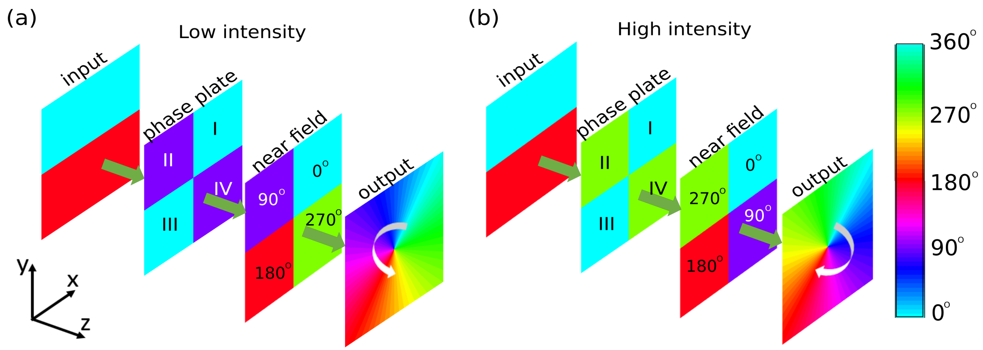
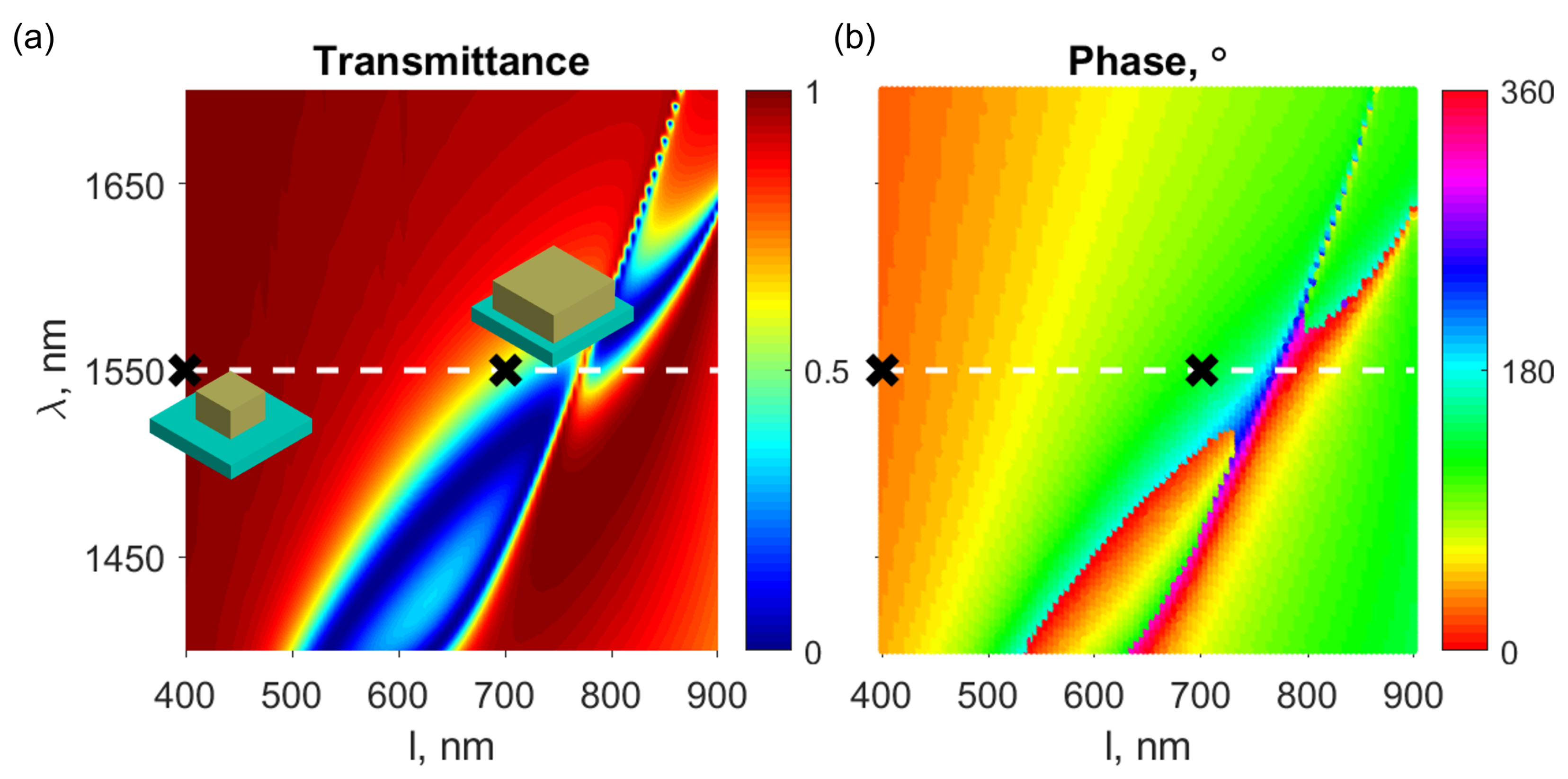
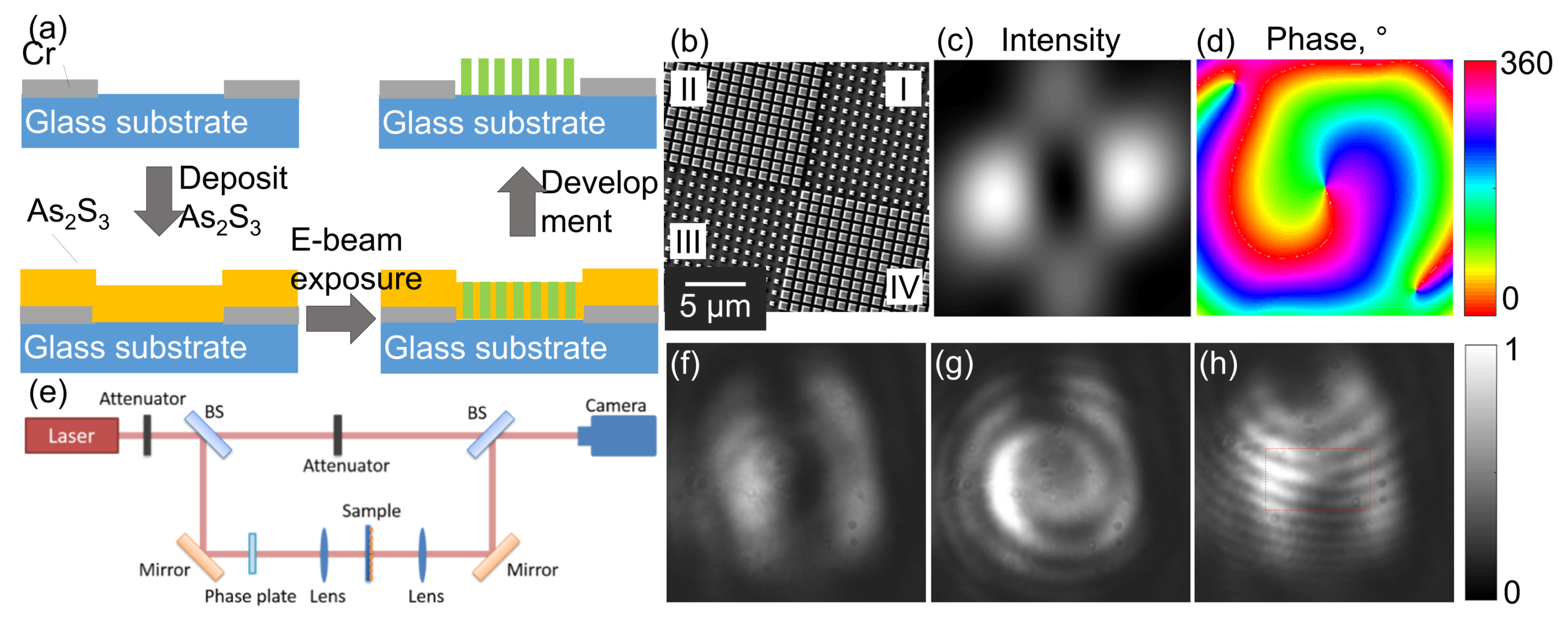
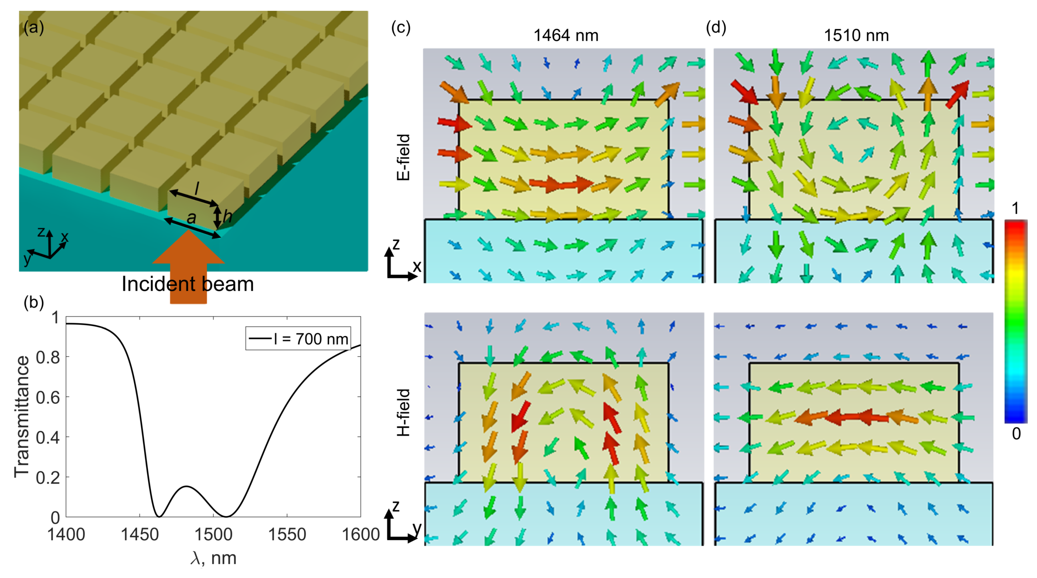
2.1. Beam-Converter Metasurface Design

The operation principle of our reconfigurable metasurface is illustrated in Figure 1. The metasurface transformed an input Hermite–Gaussian (HG) beam into an OAM beam with counter-clockwise or clockwise wavefront, depending on the intensity of the incoming light. In the linear regime—for low input intensity—the phase acquired in the even quadrants (II and IV) was 90 larger than in the odd quadrants (I and III). Consequently, the input HG beam was transmitted through the metasurface and the resulting phase distribution directly after the metasurface is given by ϕ = ( N 1 ) 90 , where N enumerated the quadrants. Although in the near-field the phase of the transmitted beam changes in a stepwise manner, in the far-field, the wavefront became helical with a counter-clockwise direction of rotation corresponding to a positive OAM, as shown in Figure 1a. Furthermore, the metasurface was designed such that for a high-intensity input beam, the phase introduced in the even quadrants was increased by 180 respect to the low-intensity regime. Figure 1b shows that in this case, the phase distribution at the output increased in the clockwise direction. In contrast with the low-intensity regime shown in Figure 1a, for high input intensity, the output beam acquired a negative OAM. The reconfigurability of the output beam was enabled by the design of the metasurface utilizing Mie-resonances in conjunction with highly nonlinear ChGs, as described below in detail.
In this section, we will demonstrate the design principle of the metasurface that converts HG beams into OAM beams. In Section 2.2, we compare the results of the experimental measurements with simulations for the mode converter operating in the linear regime, described in Section 2.1. Finally, in Section 2.3, we present a design of a nonlinear meatsuface capable of switching between the positive and negative OAM.
The functionality described in Figure 1 is enabled by a ChG-based metasurface illustrated in Figure 2a, which is an array of ChG nano-blocks fabricated on a substrate. The size of the array was assumed to be infinite in the x- and y-directions, and the incident light was a plane wave propagating along the z-axis with electric and magnetic fields polarized along the x- and y-directions, respectively. For the wavelength of interest around 1550 nm, the numerical simulations were performed by CST Microwave Studio with the following geometric parameter: the height of the blocks h = 400 nm, the lattice constant a = 930 nm, and the side-length of the blocks l = 700 nm. The refractive index of ChG was n 0 = 2.4 measured using spectroscopic ellipsometry and the refractive index of the glass substrate n g = 1.5 . Two dips located at wavelengths 1464 nm and 1510 nm corresponding to resonant interaction with the metasurfaces were indicated on the transmittance spectrum shown in Figure 2b. The near-zero transmittance resulted from a near-unity reflectance, as the materials were assumed to be lossless in the simulations. The distributions of the electric and magnetic fields in the unit cell cross-section are shown in Figure 2c,d. At the wavelength of 1464 nm, the magnetic field formed a vortex around the electric field revealing an electric resonance. At the wavelength of 1510 nm, the vortex-like electric field distribution was a signature of a magnetic resonance. As illustrated in Figure 3, in the vicinity of the central wavelengths of these resonances, the phase of the transmitted light changed rapidly by 180 .
The wavelengths corresponding to the electric and magnetic resonances can be controlled by changing the side-length of the nano-blocks. As the side-length increased, the central wavelengths of both the electric and magnetic resonances increased, and at the same time they become closer to each other. Once the two resonances overlap, a nearly unitary transmission with the phase change spanning 360 can be achieved [25,26,37]. In contrast, when the side-length decreased, the electric and magnetic resonances were shifted to shorter wavelengths and further away from the wavelength of interest. To obtain the desired phase difference for the design shown in Figure 1a, numerical simulations were performed with the side-length of the nano-block swept from l = 400 nm to l = 900 nm. Figure 3 shows the spectra of the transmittance and the phase of the transmitted light through the metasurface with different side-length for a normally incident light. We chose two different size lengths, l = 400 nm and l = 700 nm, at the wavelength of 1550 nm, as indicated with the black crosses in Figure 3. The transmittance of both structures was higher than 70 % (Figure 3a) and the phase difference between the two structures was 90 (Figure 3b).

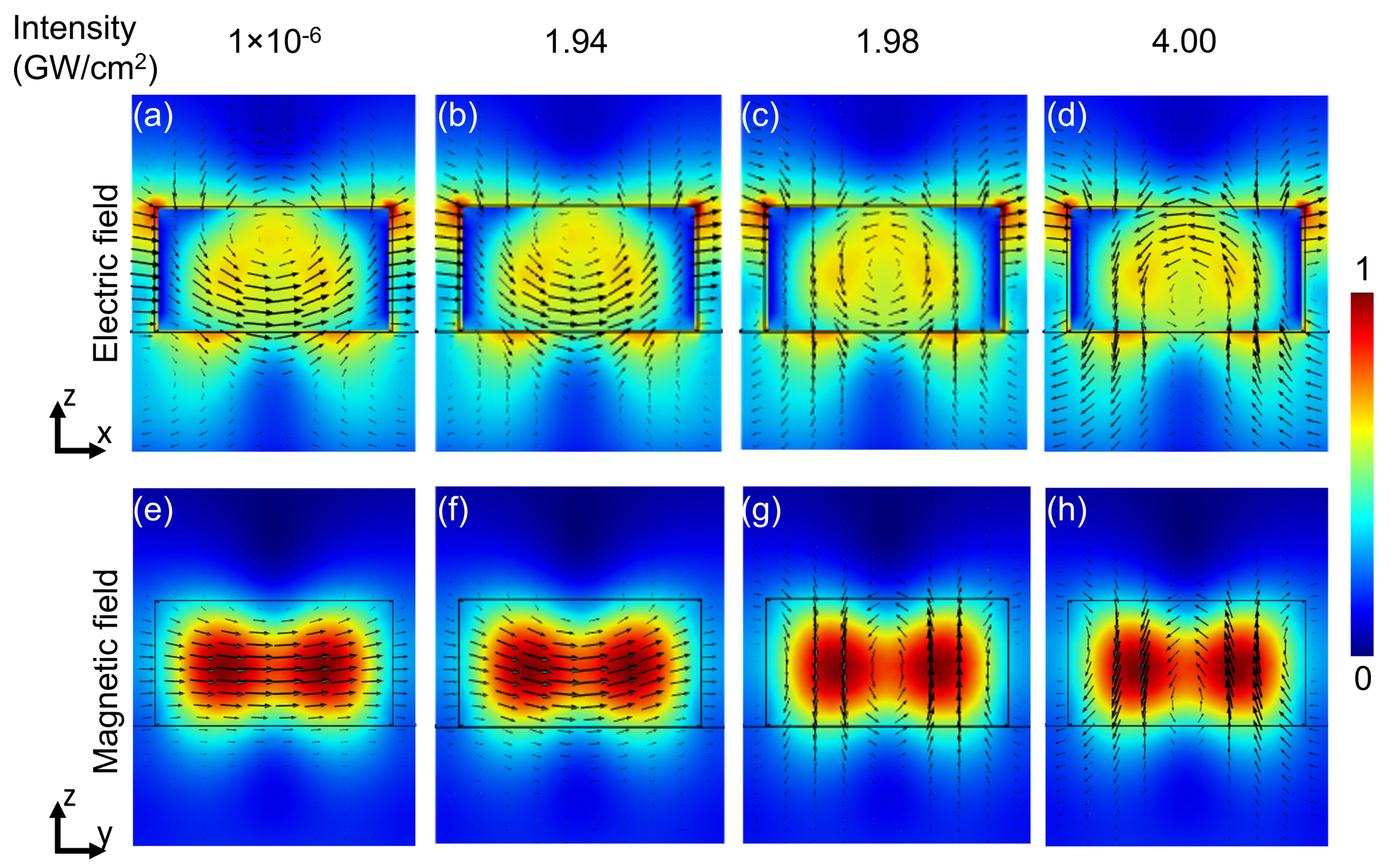
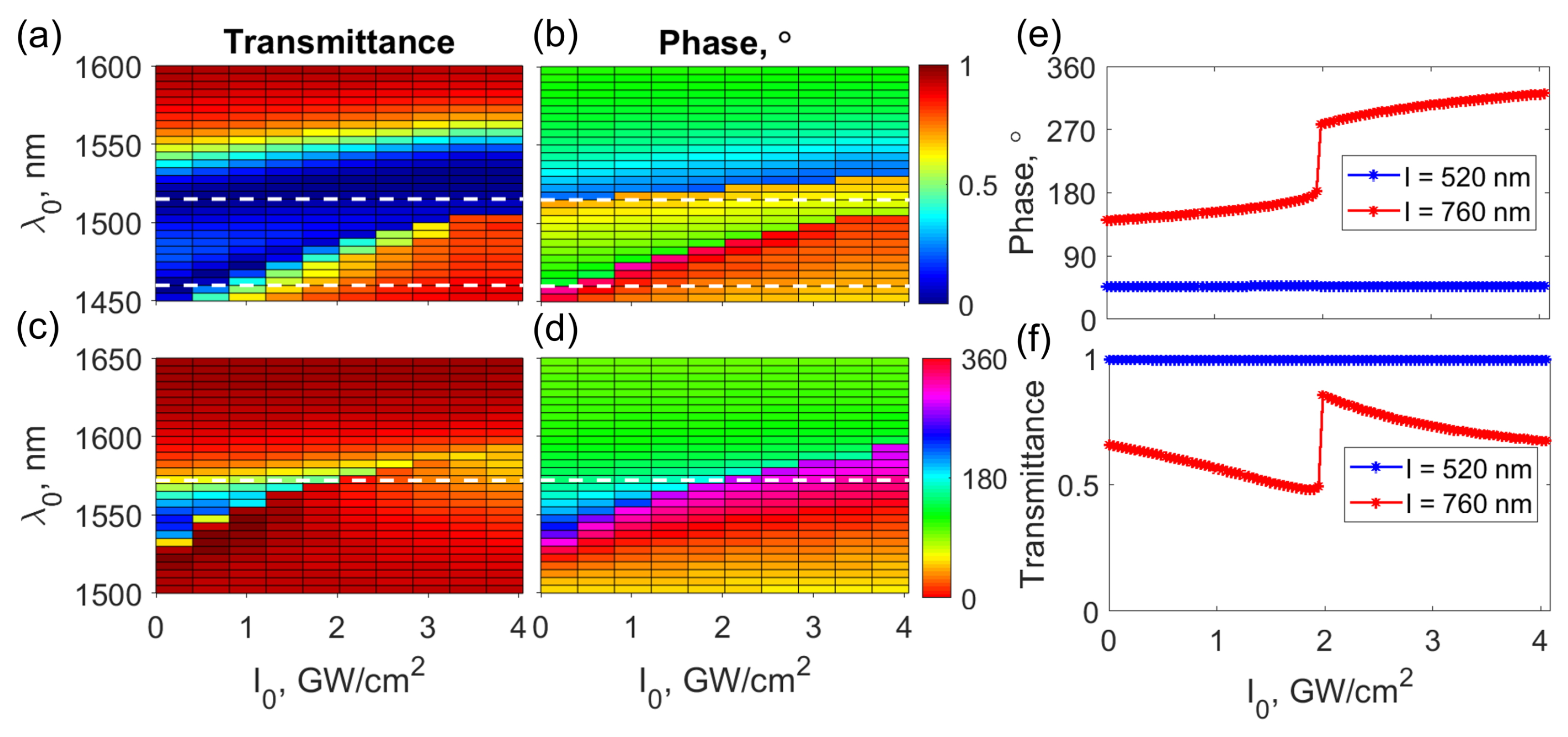
2.2. Simulations and Experiments

In order to demonstrate the proposed OAM beam-converter, a metasurface was fabricated with two sizes of the blocks l = 400 nm and l = 700 nm. The arrays of nano-blocks were patterned in ChG thin film using electron-beam lithography, as shown in Figure 4a. First, chromium windows were prepared on a glass substrate. Then, a ChG film was deposited on top of the chromium windows with thermal deposition. The linear refractive index of the film was measured using spectroscopic ellipsometry to be n 0 = 2.43 . Finally, after the exposure to electron beam, a solution of diluted MF-319 was used to develop the sample. The resulting ChG structure with a thickness of 400 nm is shown Figure 4b. The fabricated sample contains four quadrants where diagonal quadrants contain blocks with the same side-length. The total size of the fabricated metasurface was 93 μ m × 93 μ m.
The simulation of a whole metasurface consisting of four quadrants is performed with CST Microwave Studio. Then we simulate the propagation of the near-field result from CST in free space for 4 mm with the beam propagation method [38]. Figure 4c shows the normalized intensity and Figure 4d illustrates the phase of transmitted light. The spiral-shaped phase in Figure 4d proves that the wavefront of the transmitted beam is helical.
The fabricated metasurface was characterized using the interferometry setup shown in Figure 4e. The beam from a photodiode laser at the wavelength of 1550 nm was split by a beam splitter. The main beam was focused on the sample by a lens and collimated by a second lens placed after the sample. Then the main beam was combined with the reference beam using a beam splitter and the resulting interference patterns were captured by a camera. The experimental measurement of the main beam transmitted through the metasurface is shown in Figure 4f. The intensity profile with a dark singularity at the center suggests that the beam carries an OAM. In order to prove the presence of the helical wavefront, we performed two experiments on the interference of the main beam and the reference Gaussian beam. In the first experiment, after the two beams were combined, the propagating directions and centers of the Gaussian beam and main OAM beam were overlapped. The resulting interference pattern reveals spiral-shaped fringes as shown in Figure 4g. In the second experiment, a small angle was introduced between the two beams, and the interference pattern contained fork-like fringes indicating the presence of the OAM, as shown in Figure 4h.
In our previous work, the ChG hole metasurface converts an HG beam into an OAM beam by utilizing the guided resonances in a photonic crystal structure and overlapping two guided resonances to realize the desired phase shift in the even quadrants [32]. In contrast, in this experiment, the phase different between different quadrants of the fabricated metasurface is introduced by a single Mie-resonance and according to Figure 2, the resonance close to the wavelength of 1550 nm is the magnetic resonance.

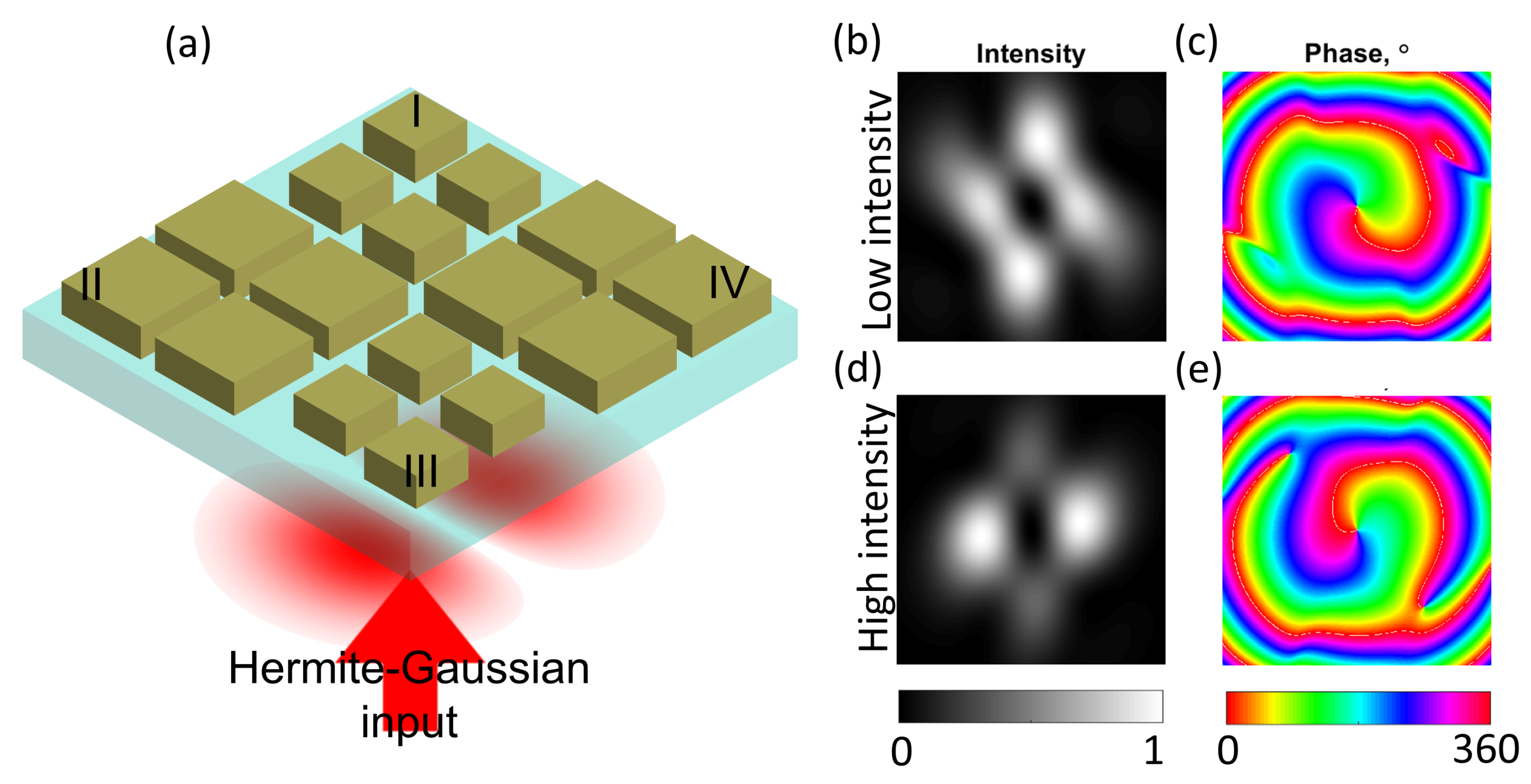
2.3. Reconfigurable Beam with OAM

In this section, we demonstrate that the third-order nonlinearity (Kerr effect) of ChG can be used to achieve the switching of the output beam OAM from positive to negative. The refractive index of the ChG n C h G can be efficiently changed as a function of the input light intensity due to its large nonlinear Kerr response described by n C h G = n 0 + Δ n = n 0 + n 2 I . Here, n 0 is the linear refractive index of the ChG, n 2 = 7.9 × 10 13 cm 2 /W is the nonlinear coefficient measured by our in-home Z-scan setup, and Δ n is the refractive index change of the ChG corresponding the input beam intensity I. Figure 5 shows the result of the nonlinear studies of ChG nano-blocks with different side-length. The input intensity was varied from 1 kW/cm 2 , which is low enough to avoid significant refractive index change, to 4 GW/cm 2 . As shown in Figure 5a,b, for l = 700 nm, around the wavelengths of electric and magnetic resonances indicated by the dashed lines, the phase change of the transmitted light is around 180 . However, at these two wavelength, the transmittance is close to zero as the two resonances are spectrally separated. Therefore, this structure is not suitable to design a nonlinear metasurface. As explained above, with the increase of the side-length, the two resonances shift closer to each other, and as they overlap, nearly 100 % transmission can be achieved with the phase change covering the entire 360 . For the side-length 760 nm, the two resonances are both located around the wavelength 1550 nm. As seen in Figure 5, the maximum 180 phase change is achieved at the wavelength of 1572 nm. This wavelength is indicated by the white dashed line in Figure 5a–d and it is the operation wavelength of the OAM beam converter. When the input intensity increases, the phase of the transmitted light changes by 180 and the transmittance at the intensity levels of interest remains higher than 60 % , as shown in Figure 5c,d. As illustrated by Figure 1, while the phase in the even quadrants changes 180 , the phase of odd quadrants should remain the same. Therefore, to realize the intensity-dependent switching, we build the odd quadrants with side-length 520 nm for which the resonances are far away from the operation wavelength of 1572 nm. As shown in Figure 5f, for low intensity 1 kW/cm 2 , the phase introduced by the structure with side-lengths of 760 nm and 520 nm differs by approximately 90 . The phase of the beam transmitted through the even quadrants (built of the cubes with the side-length of l = 760 nm) grows with the increase of the input intensity while the phase in the odd quadrants remains constant. When the intensity increases to 4 GW/cm 2 , the phase difference between the odd and even quadrants increases to 270 , while the transmittance remains higher than 60 % . Therefore, these two structures can be used to realize the proposed nonlinear metasurface enabling the intensity-dependent OAM switching. The maximum refractive index change inside ChG is Δ n = 0.12 and the maximum intensity inside the ChG blocks is 150 GW/cm 2 , as found in the simulation results. The damage threshold of ChG with different compositions measured by the femtosecond laser has been studied by Zhang et al. and You et al. at the near-infrared and mid-infrared wavelengths, respectively [39,40]. Due to the short pulse duration (100 fs) and a low repetition rate (1 KHz), the damage threshold of ChGs is much larger than the peak intensity required for our reconfigurable metasurface. Moreover, it has been reported that if As 2 S 3 is properly doped with silver, the nonlinear coefficient of the silver-doped ChG film can be up to two orders of magnitude larger than the nonlinear coefficient of the undoped As 2 S 3 film [41]. In this case, the required peak intensity will decrease to approximately 1 GW/cm 2 , making the proposed device more energy efficient. Besides energy efficiency, another advantage of the silver-doped ChG with larger nonlinear coefficient is that it may result in a much larger refractive index change Δ n . In our current design with the pure As 2 S 3 , Δ n 0.1 . Realization of a 180 phase change with the current value of Δ n 0.1 requires the resonances to be very sharp which places a stringent requirements on the fabrication precision to ensure the rapid phase change, which is beyond our ability right now. However, if a larger Δ n can be introduced by the silver-doped ChG, the design may tolerate more fabrication imperfection. The deposition and patterning processes of the silver-doped ChG film will be studied in the future to experimentally realize the reconfigurable metasurface which produces output structured light with tunable topological charges.
When the input intensity increased from 1.94 GW/cm 2 to 1.98 GW/cm 2 , the phase of the light transmitted through the structure with the side-length l = 760 nm jumped by approximately 90 , as shown in Figure 5e. The origin of this phase jump can be understood by looking at Figure 6 where the electric- and magnetic-field distributions in a unit cell for four selected input intensities are plotted. As shown in Figure 6a,b,e,f, the field distributions were very similar when the input intensity increased from 1 kW/cm 2 to 1.94 GW/cm 2 and they possess only a magnetic-resonance revealed as a vortex-like electric field distribution. When the input intensity increased, the resonances became closer to each other. In Figure 6c,d,g,h, the field distributions are very similar when the input intensity increases from 1.98 GW/cm 2 to 4 GW/cm 2 and both electric- and magnetic-resonances are present at the operation wavelength. As the light intensity increases, the electric-resonance shifts closer to the operation wavelength and as it overlaps with the magnetic resonance it leads to an abrupt phase jump by 90 . Upon the change in the input intensity from 1 kW/cm 2 to 4 GW/cm 2 , the phase changed by 180 due to the changes in the relative spectral position of the electric and magnetic resonances.
To verify the ability to produce the OAM beam with positive or negative topological charge, a metasurface with four quadrants and 50 × 50 unit cells in each quadrant was simulated using the CST Microwave Studio time domain solver and the propagating of the resulting near-field distribution in free space for 4 mm is simulated using the beam propagation method [38]. Figure 7a shows the schematic of the metasurface with an HG input beam normally incident from the substrate side. The intensity and phase distribution of the transmitted beam in low intensity case are shown in Figure 7b,c, respectively. The dark center in Figure 7b and the spiral phase distribution in Figure 7c show that the OAM is carried by the transmitted beam. In this case, the refractive index of ChG is n C h G = n 0 = 2.43 . To simulate the nonlinear metasurface, the refractive index of ChG is set as n C h G = n 0 + Δ n = 2.53 . Therefore, the phase acquired in quadrants II and IV of the metasurface changed by 180 . The light transmitted in the nonlinear regime, shown in Figure 7d,e, also has a singularity in the center, but the direction of the spiral phase distribution is opposite to Figure 7c, which means it carries an OAM with the opposite sign.

3. Summary

In this work, we have experimentally demonstrated an OAM-beam-converting metasurface enabled by the Mie-resonances of the ChG cubes operating at the telecommunication wavelength. We designed and fabricated the beam converter switching an HG mode to an OAM beam. The fabrication of the ChG film requires only single-step lithography. Moreover, ChG possesses relatively large third-order nonlinearity at near-infrared wavelengths. A nonlinear metasurface which can generate reconfigurable OAM beams with opposite topological charges is designed and demonstrated theoretically. With an HG input beam, the output of the metasurface in the linear regime has a helical wavefront and carries an OAM with topological charge plus one. When the input intensity increases to a specific value in the nonlinear regime, the output wavefront is still helical but twisted in the opposite direction than in the linear regime, which leads to a negative charge of the OAM carried by the beam. The experimental realization of the nonlinear tunable metasurface might be enabled with the use of silver-doped As 2 S 3 , which is characterized by a nonlinear coefficient two orders of magnitude larger than that of a pure As 2 S 3 film. This direction will be explored in future studies and the results will be presented elsewhere.

4. Materials and Methods

Design: we used the CST Microwave Studio Frequency Solver to design the linear metasurface. The refractive indices of materials were measured using a spectroscopic ellipsometer. The nonlinear simulations were performed in Comsol Multiphysics. The nonlinear coefficient was measured using a in-home Z-scan setup.
Sample fabrication: an array of square chromium windows with size 150 μ m × 150 μ m was fabricated on a glass substrate. Then, the As 2 S 3 film with the thickness of 500 nm was deposited on top via thermal evaporation in a Lesker PVD 75 deposition system equipped with a low temperature evaporation source. During the deposition, the substrate temperature was maintained at approximately 20 C. Inside each of the Cr windows, the ChG was patterned with a square array of blocks using electron-beam lithography (Vistec EBPG5000+ 100KV) with dosage 10.5 mC/cm 2 . The area of the pattern is 132 μ m × 132 μ m. The chromium around the sample played a double role: (i) it enhanced the reflectivity of the substrate enabling automatic sample alignment, and (ii) it increased the sample conductivity allowing us to avoid accumulation of charges. After exposure, the sample was immersed in a 1:1 mixture of Microposit MF-319 developer and deionized water for 32 seconds to develop. After the development, the parts unexposed by the electron beam have been removed and the thickness of the sample was found to be 400 nm using the atomic-force microscopy. Finally, six layers of Poly(methyl methacrylate) were spin-coated on the sample to provide a symmetric refractive index.
Experiment: to characterize the fabricated metasurface, we built a Mach–Zehnder interferometer, as shown in Figure 4e. To generate an HG mode, a phase plate was inserted in the main beam path. A glass substrate spin-coated with a layer of S1813 photoresist was used as a phase plate to delay the one part of the beam by half of the wavelength. The photoresist on half of the substrate was removed using photolithography. The edge of the photoresist was placed at the center of the main beam and a spatial light filter was placed after the phase plate to filter the HG mode.
Data availability: the data that support the findings of this study are available from the authors on reasonable request, see author contributions for specific data sets.

Author Contributions

Y.X., J.S. and N.M.L. contributed to the initial idea. Y.X., J.S., M.I.S., W.W. and A.P. performed the numerical simulation. J.F., J.D.M., R.Y.B. and J.S.S. prepared the As 2 S 3 ChG film. Y.X., J.S., M.I.S. and A.T. patterned the nanostructures on the samples. Y.X., J.S., M.I.S., W.W. and N.M.L. wrote the manuscript. N.M.L. supervised the work.

Funding

This research was funded by U.S. Office of Naval Research (N000141613020).

Conflicts of Interest

The authors declare no conflict of interest.

Abbreviations

The following abbreviations are used in this manuscript:
HGHermite–Gaussian
SLMSpatial light modulator
SPPSpiral phase plate
OAMOrbital angular momentum
ChGChalcogenide glass

References

  1. Allen, L.; Beijersbergen, M.W.; Spreeuw, R.J.C.; Woerdman, J.P. Orbital angular momentum of light and the transformation of Laguerre–Gaussian laser modes. Phys. Rev. A 1992, 45, 8185–8189. [Google Scholar] [CrossRef] [PubMed]
  2. Tamburini, F.; Mari, E.; Sponselli, A.; Thidé, B.; Bianchini, A.; Romanato, F. Encoding many channels on the same frequency through radio vorticity: First experimental test. New J. Phys. 2012, 14, 033001. [Google Scholar] [CrossRef]
  3. Wang, J.; Yang, J.Y.; Fazal, I.M.; Ahmed, N.; Yan, Y.; Huang, H.; Ren, Y.; Yue, Y.; Dolinar, S.; Tur, M.; et al. Terabit free-space data transmission employing orbital angular momentum multiplexing. Nat. Photonics 2012, 6, 488–496. [Google Scholar] [CrossRef]
  4. Willner, A.E.; Huang, H.; Yan, Y.; Ren, Y.; Ahmed, N.; Xie, G.; Bao, C.; Li, L.; Cao, Y.; Zhao, Z.; et al. Optical communications using orbital angular momentum beams. Adv. Opt. Photonics 2015, 7, 66–106. [Google Scholar] [CrossRef]
  5. Bozinovic, N.; Yue, Y.; Ren, Y.; Tur, M.; Kristensen, P.; Huang, H.; Willner, A.E.; Ramachandran, S. Terabit-Scale Orbital Angular Momentum Mode Division Multiplexing in Fibers. Science 2013, 340, 1545–1548. [Google Scholar] [CrossRef] [PubMed]
  6. Gaffoglio, R.; Cagliero, A.; Veccjo, G. Vortex Waves and Channel Capacity: Hopes and Reality. IEEE Access 2018, 6, 19814–19822. [Google Scholar] [CrossRef]
  7. Padgett, M.J. Orbital angular momentum 25 years on [Invited]. Opt. Express 2017, 25, 11265–11274. [Google Scholar] [CrossRef] [PubMed]
  8. Zürch, M.; Kern, C.; Hansinger, P.; Dreischuh, A.; Spielmann, C. Strong-field physics with singular light beams. Nat. Phys. 2012, 10, 743. [Google Scholar] [CrossRef]
  9. Sun, J.; Silahli, S.Z.; Walasik, W.; Li, Q.; Johnson, E.; Litchinitser, N.M. Nanoscale orbital angular momentum beam instabilities in engineered nonlinear colloidal media. Opt. Express 2018, 5, 5118–5125. [Google Scholar] [CrossRef]
  10. Yu, N.; Capasso, F. Flat optics with designer metasurfaces. Nat. Mater. 2014, 13, 139–150. [Google Scholar] [CrossRef]
  11. Yu, N.; Genevet, P.; Kats, M.A.; Aieta, F.; Tetienne, J.P.; Capasso, F.; Gaburro, Z. Light propagation with phase discontinuities: Generalized laws of reflection and refraction. Science 2011, 334, 333–337. [Google Scholar] [CrossRef] [PubMed]
  12. Kim, S.W.; Yee, K.J.; Abashin, M.; Pang, L.; Fainman, Y. Composite dielectric metasurfaces for phase control of vector field. Opt. Lett. 2015, 40, 2453–2456. [Google Scholar] [CrossRef] [PubMed]
  13. Minovich, A.E.; Miroshnichenko, A.E.; Bykov, A.Y.; Murzina, T.V.; Neshev, D.N.; Kivshar, Y.S. Functional and nonlinear optical metasurfaces. Laser Photon. Rev. 2015, 9, 195–213. [Google Scholar] [CrossRef]
  14. Wu, C.; Arju, N.; Kelp, G.; Fan, J.A.; Dominguez, J.; Gonzales, E.; Tutuc, E.; Brener, I.; Shvets, G. Spectrally selective chiral silicon metasurfaces based on infrared Fano resonances. Nat. Commun. 2014, 5, 3892. [Google Scholar] [CrossRef] [PubMed]
  15. Ni, X.J.; Kildishev, A.V.; Shalaev, V.M. Metasurface holograms for visible light. Nat. Commun. 2013, 4, 1–6. [Google Scholar] [CrossRef]
  16. Buchnev, O.; Podoliak, N.; Kaczmarek, M.; Zheludev, N.I.; Fedotov, V.A. Electrically controlled nanostructured metasurface loaded with liquid crystal: Toward multifunctional photonic switch. Adv. Opt. Mater. 2015, 3, 674–679. [Google Scholar] [CrossRef]
  17. Sautter, J.; Staude, I.; Decker, M.; Rusak, E.; Neshev, D.N.; Brener, I.; Kivshar, Y.S. Active tuning of all-dielectric metasurfaces. ACS Nano 2015, 9, 4308–4315. [Google Scholar] [CrossRef] [PubMed]
  18. Pfeiffer, C.; Emani, N.K.; Shaltout, A.M.; Boltasseva, A.; Shalaev, V.M.; Grbic, A. Efficient light bending with isotropic metamaterial Huygens’ surfaces. Nano Lett. 2014, 14, 2491–2497. [Google Scholar] [CrossRef]
  19. Holloway, C.L.; Kuester, E.F.; Gordon, J.A.; O’Hara, J.; Booth, J.; Smith, D.R. An overview of the theory and applications of metasurfaces: The two-dimensional equivalents of metamaterials. IEEE Antennas Propag. Mag. 2012, 54, 10–35. [Google Scholar] [CrossRef]
  20. Lin, D.; Fan, P.; Hasman, E.; Brongersma, M.L. Dielectric gradient metasurface optical elements. Science 2014, 345, 298–302. [Google Scholar] [CrossRef]
  21. Yin, X.B.; Ye, Z.L.; Rho, J.; Wang, Y.; Zhang, X. Photonic spin Hall effect at metasurfaces. Science 2013, 339, 1405–1407. [Google Scholar] [CrossRef] [PubMed]
  22. Karimi, E.; Schulz, S.A.; De Leon, I.; Qassim, H.; Upham, J.; Boyd, R.W. Generating optical orbital angular momentum at visible wavelengths using a plasmonic metasurface. Light Sci. Appl. 2014, 2, e167. [Google Scholar] [CrossRef]
  23. Zhao, Q.; Zhou, J.; Zhang, F.; Lippens, D. Mie resonance-based dielectric metamaterials. Mater. Today 2009, 12, 60–69. [Google Scholar] [CrossRef]
  24. Yao, Y.; Shankar, R.; Kats, M.A.; Song, Y.; Kong, J.; Loncar, M.; Capasso, F. Electrically tunable metasurface perfect absorbers for ultrathin mid-infrared optical modulators. Nano Lett. 2014, 14, 6526–6532. [Google Scholar] [CrossRef] [PubMed]
  25. Shalaev, M.I.; Sun, J.; Tsukernik, A.; Pandey, A.; Nikolskiy, K.; Litchinitser, N.M. High-Efficiency All-Dielectric Metasurfaces for Ultracompact Beam Manipulation in Transmission Mode. Nano Lett. 2015, 15, 6261–6266. [Google Scholar] [CrossRef] [PubMed]
  26. Fu, Y.H.; Kuznetsov, A.I.; Miroshnichenko, A.E.; Yu, Y.F.; Luk’yanchuk, B. Directional visible light scattering by silicon nanoparticles. Nat. Commun. 2013, 4, 1527. [Google Scholar] [CrossRef] [PubMed]
  27. Lapine, M.; Shadrivov, I.V.; Kivshar, Y.S. Colloquium: Nonlinear metamaterials. Rev. Mod. Phys. 2014, 86, 1093. [Google Scholar] [CrossRef]
  28. Shadrivov, I.V.; Kapitanova, P.V.; Maslovski, S.I.; Kivshar, Y.S. Metamaterials controlled with light. Phys. Rev. Lett. 2012, 109, 083902. [Google Scholar] [CrossRef]
  29. Pandey, A.; Litchinitser, N.M. Nonlinear light concentrators. Opt. Lett. 2012, 37, 5238–5240. [Google Scholar] [CrossRef]
  30. Shcherbakov, M.R.; Vabishchevich, P.P.; Shorokhov, A.S.; Chong, K.E.; Choi, D.Y.; Staude, I.; Miroshnichenko, A.E.; Neshev, D.N.; Fedyanin, A.A.; Kivshar, Y.S. Ultrafast all-optical switching with magnetic resonances in nonlinear dielectric nanostructures. Nano Lett. 2015, 15, 6985–6990. [Google Scholar] [CrossRef]
  31. Shcherbakov, M.R.; Liu, S.; Zubyuk, V.V.; Vaskin, A.; Vabishchevich, P.P.; Keeler, G.; Pertsch, T.; Dolgova, T.V.; Staude, I.; Brener, I.; et al. Ultrafast all-optical tuning of direct-gap semiconductor metasurfaces. Nat. Commun. 2017, 8, 17. [Google Scholar] [CrossRef] [PubMed]
  32. Xu, Y.; Sun, J.; Frantz, J.; Shalaev, M.I.; Walasik, W.; Pandey, A.; Myers, J.D.; Bekele, R.Y.; Tsukernik, A.; Sanghera, J.S.; et al. Reconfiguring structured light beams using nonlinear metasurfaces. Opt. Express 2018, 23, 30930–30943. [Google Scholar] [CrossRef] [PubMed]
  33. Sanghera, J.S.; Shaw, L.B.; Pureza, P.; Nguyen, V.Q.; Gibson, D.; Busse, L.; Aggarwal, I.D.; Florea, C.M.; Kung, F.H. Nonlinear properties of chalcogenide glass fibers. Int. J. Appl. Glass SCI 2010, 1, 296–308. [Google Scholar] [CrossRef]
  34. Eggleton, B.J.; Luther–Davies, B.; Richardson, K. Chalcogenide photonics. Nat. Photonics 2011, 5, 141–148. [Google Scholar] [CrossRef]
  35. Hilton, A.R.; Kemp, S. Chalcogenide Glasses for Infra-Red Optics; McGraw Hill: New York, NY, USA, 2010. [Google Scholar]
  36. Vlcek, M.; Jain, H. Nanostructuring of chalcogenide glasses using electron beam lithography. J. Optoelectron. Adv. Mater. 2006, 8, 2108–2111. [Google Scholar]
  37. Van de Groep, J.; Polman, A. Designing dielectric resonators on substrates: Combining magnetic and electric resonances. Opt. Express 2013, 21, 26285–26302. [Google Scholar] [CrossRef]
  38. Feit, M.D.; Fleck, J.A. Light propagation in graded-index optical fibers. Appl. Opt. 1978, 17, 3990–3998. [Google Scholar] [CrossRef]
  39. Zhang, M.; Li, T.; Yang, Y.; Tao, H.; Zhang, X.; Yuan, X.; Yang, Z. Femtosecond laser induced damage on Ge–As–S chalcogenide glasses. Opt. Mater. Express 2019, 2, 352213. [Google Scholar] [CrossRef]
  40. You, C.; Dai, S.; Zhang, P.; Xu, Y.; Wang, Y.; Xu, D.; Wang, R. Mid-infrared femtosecond laserinduced damages in As2S3 and As2Se3 chalcogenide glasses. Sci. Rep. 2017, 7, 6497. [Google Scholar] [CrossRef]
  41. Kosa, T.I.; Rangel–Rojo, R.; Hajto, E.; Ewen, P.J.S.; Owen, A.E.; Kar, A.K.; Wherrett, B.S. Nonlinear optical properties of silver-doped As2S3. J. Non-Cryst. Solids 1993, 164, 1219–1222. [Google Scholar] [CrossRef]
Figure 1. Working principle of a nonlinear metasurface with reconfigurable output beam. The color maps show the phase of the input and output beams, and the phase shifts introduced by the metasurface. (a) At low intensity, upon transmission through the metasurface, the input Hermite–Gaussian (HG) beam acquires a non-uniform phase distribution leading to generation of a beam carrying a positive orbital angular momentum (OAM). (b) At high intensity, the phase in even quadrants changes by 180 ; the output beam possesses a negative OAM, as opposed to the low-intensity case.
Applsci 09 00958 g001
Figure 2. Design of the metasurface. (a) Metasurface consisting of a square lattice of square-blocks made of arsenic trisulfide (As 2 S 3 ) chalcogenide glass (ChG) on a glass substrate. The geometric parameters of the metasurface are: height h = 400 nm; lattice constant a = 930 nm; and the side-length of the blocks is denoted by l. The refractive index of the ChG film is n 0 = 2.43 . The refractive index of glass is n g = 1.5 . (b) The transmittance of an array of ChG blocks with l = 700 nm. Two resonances are indicated at the wavelengths of 1464 nm and 1510 nm. (c) Electric and magnetic fields in the center of the unit cell (cross-section y = 0 ) at the wavelength of 1464 nm. (d) Electric and magnetic fields in the center of the unit cell (cross-section x = 0 ) at the wavelength of 1510 nm.
Applsci 09 00958 g002
Figure 3. Spectral dependencies of (a) the transmittance and (b) the phase of the transmitted light as a function of the side-length, revealing the presence of Mie resonances. The dashed line indicates the operation wavelength λ 0 = 1550 nm. The two black crosses indicate the parameters used for the metasurface beam converter design.
Applsci 09 00958 g003
Figure 4. (a) Fabrication process for ChG-based all dielectric metasurfaces involves the following steps: fabrication of a chromium window with the size of 150 μ m × 150 μ m; deposition of an As 2 S 3 film; exposure of the As 2 S 3 using electron beam; development of the exposed sample. (b) Scanning electron microscopy image of the fabricated metasurface with four quadrants. (c) Intensity and (d) phase of simulation results of an HG beam transmitted through the metasurface. (e) Schematic of the Mach–Zehner interferometer used to characterize the fabricated metasurface. (fh) Experimental results obtained with the fabricated metasurface. (f) Intensity distribution of the output OAM beam. (g,h) Interference of the output OAM beam and a reference Gaussian beam showing a spiral-shaped and fork-like intensity distributions (see text for details).
Applsci 09 00958 g004
Figure 5. Nonlinear study results of ChG nano-blocks. (a) Transmittance and (b) phase of transmitted light with side-length 700 nm. (c) Transmittance and (d) phase of transmitted light with side-length 760 nm. (e) Transmittance and (f) phase of transmitted light with side-length l = 520 nm and l = 760 nm at the operation wavelength of 1572 nm.
Applsci 09 00958 g005
Figure 6. Normalized electric (ad) and magnetic fields (eh) at four selected input intensities. The input intensities are labeled on the top. Both the arrow length and the color maps represent the field intensity. The color plots are normalized to the maximum value on each plot. Panels (a,b,e,f) show that before the phase jump, only a magnetic resonance is present at the operation wavelength. When the intensity increases, both resonances shift to longer wavelengths; panels (c,d,g,h) show that for intensity larger than 1.98 GW/cm 2 both electric and magnetic resonances are present at the operation wavelength, which results in the 90 phase jump.
Applsci 09 00958 g006
Figure 7. Schematic and simulation results of the nonlinear tunable metasurface. (a) Schematic of a metasurface consisting of four quadrants with an HG input beam incident from the bottom. (b) Intensity and (c) phase distribution of the light transmitted through the metasurface at low intensity. The refractive index of ChG is n C h G = n 0 = 2.43 . (d) Intensity and (e) phase distribution of the light transmitted through the metasurface at high intensity. The refractive index of ChG is assumed to be uniform and to have a value n C h G = n 0 + Δ n = 2.53 .
Applsci 09 00958 g007

