Lossless WDM PON Photonic Integrated Receivers Including SOAs
by
 , and
, and
Pantea Nadimi Goki
1,*, 
Muhammad Imran
1,
Claudio Porzi
1,
Veronica Toccafondo
2,
Francesco Fresi
2,
Fabio Cavaliere
3 and
and
Luca Potì
2 1
TECIP Institute Scuola Superiore Sant’Anna, 56124 Pisa, Italy
2
CNIT Photonic Networks and Technologies Nat’l Lab, 56124 Pisa, Italy
3
Ericsson, 56124 Pisa, Italy
*
Author to whom correspondence should be addressed.
Appl. Sci. 2019, 9(12), 2457; https://doi.org/10.3390/app9122457
Submission received: 29 March 2019
/
Revised: 31 May 2019
/
Accepted: 12 June 2019
/
Published: 15 June 2019
(This article belongs to the Special Issue PICs for Optical Interconnects)
Abstract
:The role of a semiconductor optical amplifier (SOA) for amplifying downstream traffic at optical network terminals (ONT) within a silicon-photonics integrated receiver in a high capacity passive optical network (PON) is investigated. The nearly traveling wave SOA effects are evaluated by considering fabrication and link loss constraints through numerical analysis and experimental validation. The impact of hybrid integration of a SOA chip on a silicon on insulator (SOI) photonic chip using the flip chip bonding technique on SOA design is evaluated through numerical analysis of a multi section cavity model. The performance of the proposed ONT receiver design employing twin parallel SOAs is evaluated experimentally on a 32 × 25 Gb/s OOK WDM transmission system considering cross gain modulation (XGM) and amplified spontaneous emission (ASE) constraints. The XGM impact is evaluated through 32 channel wavelength division multiplexing (WDM) transmission and a likely PON worst case scenario of high channel power difference (~10 dB) between adjacent channels. The impact of ASE is evaluated through the worst-case polarization condition, i.e., when all of the signal is coupled to only one. Successful transmission was achieved in both worst-case conditions with limited impact on performance. SOA results indicate that a maximum residual facet reflectivity of 4 × 10⁻⁴ for the chip-bonded device can lead to a power penalty below 2 dB in a polarization-diversity twin SOAs receiver.
1. Introduction
Technological innovations are continuously introducing novel applications that greatly influence the way humans interact, make decisions and conduct businesses. It is estimated that traffic from wireless devices will account for more than 63 percent of total IP traffic by 2021 [1]. These applications demand enhanced capacity, coverage, low latency and high quality of service (QoS) from wireless as well as optical access networks. Optical fiber distribution networks (ODN) in already installed passive optical access networks (PON) can be exploited to cope with diverse traffic demands originated from 5G mobile fronthaul, backhaul and large capacity short reach point to point links [2]. Designing low cost, low complexity and high capacity short reach PON access links using ODNs is a challenging task due to high link loss, particularly for optical network terminals (ONTs) at the customer premises. ONT transmitter complex modulation formats can provide higher capacity (>10 Gb/s) but keeping conventional non-return-to-zero (NRZ) modulation is a better option for low complexity and cost. However, conventional PIN-TIA receivers have low sensitivity, therefore power budget and higher capacity cannot be managed at the same time. Alternatively, receivers employing avalanche photodiodes (APD) and TIA have been demonstrated for 25 Gb/s TDM-PON links, but these kinds of APDs are not yet widely commercially available [3,4]. In this scenario, optical amplification becomes essential. Erbium doped fiber amplifiers (EDFA) at the optical line terminal (OLT) can amplify all downstream traffic, but integrated semiconductor optical amplifiers (SOAs) are a better choice at the ONTs due to having a smaller footprint despite relatively higher noise. Moreover, SOA-PIN/TIA receivers have a relatively large margin in terms of bandwidth improvement compared to APDs and can be realized at any telecom wavelength [5]. A recent study about the applicability of SOAs in PONs concluded that managing the optical power budget (>29 dB) for greater than 10 Gb/s PON such as 25 Gb/s and 50 Gb/s while using state-of-the-art low-cost components is challenging and will require pre/booster or both amplifiers [6]. Monolithic III-V photonic integrated pre-amplified optical receivers that integrate SOA and photodiodes [7,8] and TIA [9] have already been demonstrated for up to 40 Gb/s high speed PONs. Among the different photonic integration technologies, silicon photonics is particularly promising for ONT transceivers due to large scale integration capability, low cost, and reliability. Hybrid integration of SOA and mode locked laser in an eight channel WDM silicon photonic transceiver using edge coupling was recently reported in [10]. Nevertheless, hybrid integration of InP-based SOAs on silicon-on-insulator (SOI) substrates using flip-chip bonding [11,12] techniques poses additional challenges in the design of SOA devices, as it affects important parameters such as effective reflectivity, coupling efficiency, and gain ripples.
Design of SOA devices combined in photonic integrated circuits (PICs) required precise numerical modeling and optimization of existing models. Several numerical models have been proposed for calculation/estimation of SOA parameters and operational behavior [13,14]. Vagionas et al. [15] presented experimentally validated SOA numerical modeling techniques applicable to a wide range of SOA devices by using the transfer matrix method (TMM). In [16], they reported an optimized SOA model using the transmission line matrix (TLM) method to simulate light propagation through the active region of SOA. Shawki et al. described a theoretical model of the SOA time domain oscillation dynamics, used for the simulation of the oscillation dynamics in the SOA-based random laser [17]. A wideband steady-state model of a strained MQW-SOA has been described in [18], which uses an asymmetric broadening function in the material gain and additive spontaneous emission calculations. In [19], a numerical model was reported for the simulation of all nonlinear effects of the SOA. All these models proposed to optimize the operating conditions and improve SOA design, either stand-alone or on chip, for different applications. Depending on the application, SOAs are operated either in linear regime, as in-line amplifiers in optical communication networks [20,21] or in nonlinear regime, as all optical logic gates [22], all-optical switching [23] and wavelength conversion [24]. SOA performance has been investigated in terms of input signal with different modulation formats, different input pulse shapes [25,26] and nonlinear pulse propagation [27].
In this paper, we propose an architecture of a lossless polarization insensitive hybrid photonic integrated WDM PON ONT receiver that employs SOAs. The proposed SOAs not only compensate the link loss but also compensate the on-chip losses. Dual polarization grating couplers and the twin parallel SOA structure provides polarization insensitive design. SOI based tunable micro-ring filters are proposed to drop the relevant wavelength. We investigate the design of a SOA device for bidirectional 32 × 25 Gb/s short reach optical access links through numerical simulation modelling. The optimum SOA device parameters and dimensions are evaluated under ODN link loss and integrated ONT receiver fabrication constraints on a reference architecture. Steady state and dynamic analysis are also performed to evaluate WDM transmission performance. We also validate our model experimentally, using commercial SOAs in realistic working conditions. The impact of cross gain modulation (XGM) and amplified spontaneous emission (ASE) on receiver performance is also evaluated experimentally in worst case power and polarization imbalance conditions.
2. Lossless WDM PON Architectural Model
The lossless WDM PON architectural model considered for simulation and experimental investigation in this work is shown in Figure 1. The architecture consists of generic PON network elements; OLT, ODN and ONT with an additional proposed photonic integrated receiver including twin parallel SOAs. The architecture can support 32 bidirectional C-band DWDM channels that are transmitted at 25 Gbit/s with 50 GHz-interleaved downstream/upstream channel spacing. The OLT consists of arrays of transmitters and receivers, mux/demux and pre- and booster-EDFAs. The ODN length is 15–20 km and split ratio is 32. To maintain compliance to safety class 1M, the maximum overall output power considered for the OLT booster amplifier is 21 dBm, corresponding to up to 6 dBm per channel. Considering 2 dB for circulator and band split loss, the reference launch power per channel is 4 dBm. The overall expected loss including the ODN, circulator and band splitter (at receiver) is expected to be about 25–30 dB considering the typical loss for fibers and passive components. The ONT has a tunable transmitter for upstream and an integrated receiver. At the receiver, the WDM multiplexed channels are coupled to the SOA and one of the channels is dropped using a relevant micro-ring resonator based tunable filter before detection and conversion into output electrical signal [28]. Receiver sensitivity is considered to be −16 dBm and target optical signal-to-noise ratio (OSNR) is 19 dB. A polarization insensitive scheme for the integrated receiver can be realized by exploiting twin parallel SOAs and filters: the optical signal is coupled to the photonic integrated chip through dual polarization grating couplers (GC) [29], separating the transverse electric (TE) and transverse magnetic (TM) modes over two different waveguides feeding two twin parallel SOAs. It is assumed that SOAs are placed in the SOI trench using the flip-chip technique. The light between the SOA and other silicon components is coupled through a spot size converter. The SOA is designed to compensate the link, coupling and on-chip losses.
3. SOA Design, Modelling and Analysis
Due to unavoidable non-perfect mode matching at the interface between the spot-size converter and the SOA, the usual travelling-wave assumption for the amplifier is no longer strictly valid, and even small reflections need to be taken into account. In this work we consider a nearly traveling wave (NTW) semiconductor optical amplifier [30] design for 16.5 dB gain at peak wavelength, large gain bandwidth of around 150 nm, and <1 dB gain ripple. Both steady state and dynamic analysis is performed for optimum SOA design using a parabolic gain model.
Under proper forward biasing of the device, amplification occurs in the active region of the SOA, so that the signal experiences a single pass gain Gsp = exp(gL), where g is the net gain per unit length which includes the material gain coefficient per unit length gm = a(n − n0 ) − a2(λ − λp)2, being a and a2 the differential gain coefficient and gain constant, respectively, n and n0 the injected and transparency carrier densities, respectively, and λp the peak gain wavelength [31]. The amplification factor for a resonant amplifier is defined by [30,32]:
where φ is the total single-pass (carrier-dependent) phase shift, and R1 and R2 are facet reflectivities. The NTW regime of operation for the amplifiers is defined as the condition for which the gain ripples ΔG are below 3 dB, which requires residual facet reflectivities (RFR) such that [30]. Figure 2 shows the simulated spectral characteristic of the amplifier gain, for which the gain ripples due to residual facet reflectivities are within about 0.3 dB. In this simulation, the SOA single pass gain Gsp is about 16.5 dB, and facet reflectivities are R1 = R2 = 4 × 10⁻⁴. The RFR is such that Gsp × R = 0.017, corresponding to ΔG = 0.3 dB, which is in good agreement with the experimentally measured gain profile.
In order to extrapolate relevant parameters to be used in the simulation, we performed measurements from a real device. In particular, the active region length has been obtained from the measured free-spectral range (FSR) of the ASE ripples as [33]:
where is the central wavelength (1500 nm), is the average semiconductor refractive index and ∆λ is the FSR (0.2 nm). Since the ASE is proportional to the amplifier gain (G), the gain ripple can be directly measured on the ASE spectrum [34]. The active region length was obtained by measuring the wavelength spacing between two maxima of the ASE spectrum ripples. The gain profile is shown in Figure 3 together with the simulated one; the peak gain of 16.5 is measured at 1500 nm and the gain at 1550 nm is around 15 dB. The simulated curve is in good agreement with the measured one in the region above the peak wavelength (i.e., around the operating wavelength of 1550 nm), whereas there is little difference between the measured and simulated gain profile below the peak wavelength. Besides the obvious approximation introduced by the parabolic model, this mismatch is also ascribed to the gain tilting effect in the SOA under the broadband light injection used for the measurement. Furthermore, as the wavelength is further lowered from the peak, the measurement is dominated by the noise floor and sensitivity of the system, due to the limited amount of spectral power from the broadband ASE source. This causes the observed inversion in the expected gain drop at short wavelengths.
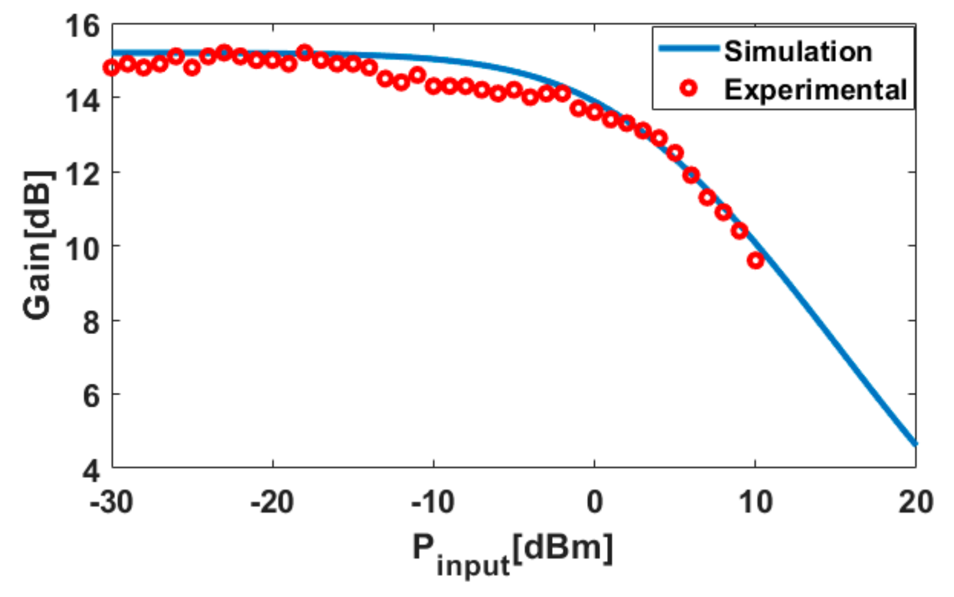
The SOA gain as a function of input power was also investigated at a wavelength of 1550. The small-signal gain of the SOA device is measured to be 15.25 dB. The gain reduction characteristic as a function of input power due to carrier depletion in the active region has also been measured, providing a saturation input power , at which the gain is reduced by 3 dB, of 5.2 dBm. Signal distortion will occur when the output optical power becomes comparable to the saturation power of the amplifier [35,36], defined by:
where is the Plank constant, is the optical frequency, is the active region cross section, where W and d are its width and thickness, respectively, is the optical confinement factor, is the carrier life time and is the already introduced differential gain coefficient. By using the following equation, the SOA gain as a function of input power was obtained [37]:
where is the (small-signal) unsaturated amplifier gain, and is the input amplifier power, which can be defined as a function of output power where is the output amplifier power. Figure 4 shows the simulated and the experimentally measured gain saturation characteristics for a wavelength of 1550 nm at an injection current of 500 mA. The simulation results are in good agreement with the experimentally measured gain values. It should be noted that the device used in the experiment was a relatively dated one. Current SOA technology is able to provide similar values of small signal gain and output saturation power with driving current in the order of 200 mA.
The dynamic model used to simulate the NTW SOA is similar to the model used in [38], which is based on the numerical solution of the rate equation for carrier density. The model can be easily updated to include nonlinear gain compression terms [15] to investigate operation under strong saturation regimes as well. For the modal gain, a fitted parabolic model was used:
where cv is a parameter related to the bandwidth of the modal gain, and λgap is the band-gap optical wavelength. To perform dynamic simulations, the SOA was divided into a sufficiently large number of sections, so that the carrier concentration density within each section can be considered constant. Starting from the first section, where the input signal is considered, the solution of the time-dependent carrier rate equation for each section is used to calculate the signal at the input of the subsequent section. To solve the rate equations of each section, a standard ordinary differential equation (ODE) is used. The SOA model parameters used for simulations are presented in Table 1.
In the present paper, the effect of the amplified spontaneous emission to the SOA output signal was added as Gaussian noise with variance equal to the ASE power. The spontaneous emission power can be written as [39]:
where is the spontaneous emission factor and is the optical filter bandwidth. The factor of two accounts for the unpolarized nature of ASE [40]. The effects of ASE on the carrier dynamics in the semiconductor optical amplifier can be accounted for by using the models presented in [41,42].
Equivalent Cavity and Reflectivity Design
A multi section cavity analysis has been performed to optimize the SOA model by incorporating flip chip technique assembly constraints in terms of its effective reflectivity. We took into account the multi-cavity effect due to discontinuities in the hybrid integrated SOA–SOI chip by using effective mirror model and scattering-matrix analysis [43]. In Figure 5, an equivalent mirror cavity is depicted, which replaces the SOI waveguide passive section by an effective mirror with reflectivity reff. In particular, the reflectivity from the spot-size converter taper between the SOA and SOI waveguide and from the input/output GC reflectivity have been considered in order to compute the effective complex facet reflectivity reff as:
where and are the reflection and transmission coefficient at the spot-size converter taper part respectively, is reflection at GC, is the complex propagation constant, is the effective index and is passive cavity internal loss. This yielded the value for the residual facet reflectivity R = |reff|2 (assuming reff1 = reff2) of the SOA that needs to be considered in Equation (1) for ensuring a reduced ripple amplitude of 0.3 dB. Figure 6 shows the contour plot for the calculated RFR versus GC and tapered section reflectivities. The plot has been obtained using SOA with an active region length of 1600 µm assembled to the SOI waveguide with 2600 µm passive cavity length from each side.
4. Results
4.1. Transmission Simulation
The performance of the designed SOA device in the reference DWDM architecture was evaluated through simulation of a 32 × 25 Gb/s NRZ transmission with 100 GHz channel spacing and 211-1 pseudo-random bit sequences (PRBS) data. The input power to the SOA was −20 dBm per channel.
The receiver scheme with twin parallel SOAs was considered: the incident signal is split into two orthogonal polarization states, TE and TM, and each one of them is amplified by separate SOAs. The transmission performance was evaluated under the worst case scenario, i.e., the incident signal has only one polarized state and all light is coupled to only one SOA while the twin SOA works in the absence of input signal. In this condition, the second SOA only emits ASE noise at the output which is coupled with the amplified signal from the first SOA. The transmission performance for a channel under test (Ch.u.t.) was evaluated through eye diagrams either in the presence or absence of the second SOA to assess the impact of the additional ASE noise. Clear eye opening shows successful transmission of 32 WDM channels (Figure 7) with a limited impact of the ASE due to the second SOA.
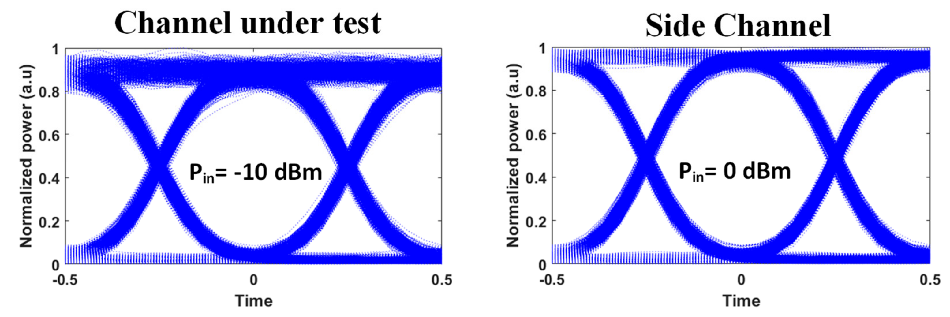
We also considered another potentially critical scenario where power differences of two adjacent input channels is about 10 dB in order to estimate the impact of XGM. Figure 8 shows the eye diagrams for the Ch.u.t. (left) and its 10 dB stronger side channel (right) for the case of input power of −16 dBm and −6 dBm respectively. There is no evidence of XGM and pattern effects are visible.
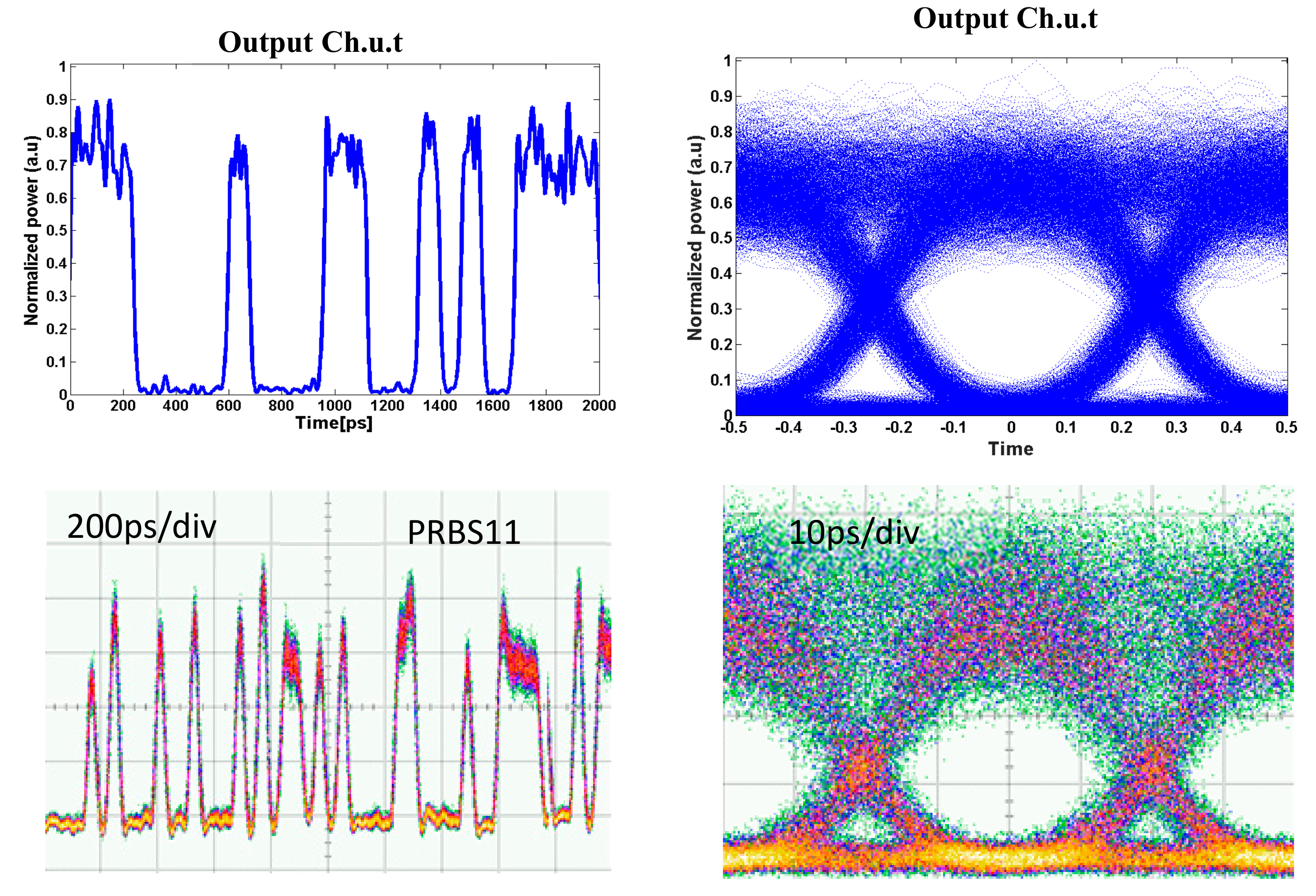
To evaluate the model for SOA operation in nonlinear regime (NL), we also simulated transmission of 32 × 25 Gb/s with −4 dBm input power per channel. Such a large input power causes the SOA to switch into the NL regime and represents a large cross gain modulation (XGM). The signal quality is affected by patterning due to gain saturation. The nonlinear effect on the data pattern and eye diagram of the Ch.u.t is depicted in Figure 9.
4.2. Experimental Results
The experimental setup for validation of the developed software model is shown in Figure 10. The 25 Gb/s NRZ signal for the Ch.u.t. was generated by exploiting an Mach-Zehnder modulator (MZM) fed with a continuous wave (CW) laser at 1552 nm and driven by a bit pattern generator (BPG) with a 231-1 PRBS. A second MZM was fed by 16 CW lasers spaced by 200 GHz and driven by a second bit pattern generator (BPG) with a 25 Gb/s 231-1 PRBS to generate the interfering channels. The channel allocation on the SOA gain curve is shown in Figure 11.
Ch.u.t. and interfering channels were coupled together and to emulate the effect of 32 channels, we reduced the power of the Ch.u.t. by 3 dB with respect to the interfering channels. The worst case for XGM has been considered here as the interfering channels are all modulated with the same data stream. Two identical SOAs have been used in the experiment to implement the polarization-diversity scheme with twin coupled SOAs.
To emulate the worst case polarization condition, the optical signal is fed to the first SOA only (with optimized polarization) while the second SOA works in the absence of input power and emits ASE noise only. Both SOAs are biased at 500 mA. Total input power for SOA1 is set to −5 dBm (corresponding to −20 dBm for Ch.u.t.). After the 3 dB coupler, the Ch.u.t. power is −8 dBm, far above the receiver sensitivity of −16 dBm of the reference architecture. A 1 nm optical band-pass filter (OBPF) was used to extract the Ch.u.t. for eye-diagram evaluation and bit-error-rate (BER) measurements. At the receiver, a 30 GHz photo receiver was used, followed by a 45 GHz oscilloscope and a 25 Gb/s error detector. Unfortunately, due to the high insertion loss (6 dB) of the OBPF used in the experiment and the receiver sensitivity of the available photoreceiver (−10 dBm), the thermal noise was dominating the ASE noise of the SOAs and hiding other possible impairments. This required the use of a pre-amplified receiver to accurately evaluate the impact of the SOAs in absence of the receiver thermal noise.
Figure 10 reports the eye diagrams of the Ch.u.t. in back-to-back, after SOA1 and after coupling with SOA2 cases. BER has been evaluated by varying the optical power at the input of the pre-amplified receiver.
To highlight the impact of the two SOAs, both cases of a single SOA and twin SOAs have been considered. Experimental BER results are shown in Figure 12. The curves show that at BER = 1 × 10⁻⁹, there is only a 2 dB penalty for the twin SOAs scheme.
In order to examine the device’s nonlinear behavior performance in terms of cross gain modulation (XGM), we injected two signals to the SOA with −20 dBm (Ch.u.t at 1552 nm) and +5 dBm (3 × 0.8 nm from Ch.u.t) optical input power, respectively. Both signals were modulated to produce a 25 Gb/s 211-1 PRBS sequence. The results of the simulated and measured signal of the channel under test are depicted in Figure 13. Since the available SOA is linear with high saturation input power of +6 dBm, within this optical power range, the eye diagram does not exhibit a significant nonlinear effect.
5. Conclusions
SOA is a promising approach to optimize performance for future PON due to the wide gain bandwidth, low-price and high integration capability. We proposed a practical scheme for a polarization-insensitive integrated receiver including twin parallel SOAs for the ONT receiver. We evaluated optimum design considerations for integrated WDM 25 Gb/s integrated ONT receivers exploiting SOAs under ODN loss. The SOA in the receiver are designed not only to compensate the coupling and link losses, but also on chip losses to realize the lossless receiver design. We performed a multi section cavity analysis for optimum SOA model design to incorporate the flip chip technique constraints. The bonding constraints of SOA in the hybrid integrated SOA–SOI chip for obtaining lower gain ripples (∆G) were evaluated. The effect of ASE noise as well as the XGM on an amplified optical signal using twin parallel SOAs was modeled for linear and nonlinear behavior investigation of the SOA construct. The XGM impact is investigated using 32 × 25 Gb/s channels as well as considering two adjacent input channels where the interfering channel is 10 dB higher, without significant impairments as long as the input power remains below approximately 6 dBm. Transmission performance and ASE effect were evaluated in the worst-case polarization condition, i.e., when all of the signal is coupled to one SOA, which resulted in the successful transmission of 32 WDM channels with a limited impact of the ASE due to the second SOA.
Author Contributions
P.N.G.; F.F.; and V.T.; designed and performed the experiments, C.P.; designed and modeled SOA simulations. P.N.G.; performed the simulations and with C.P.; analyzed the results. F.C.; provided vendor specifications. P.N.G.; M.I.; F.F.; and C.P.; wrote the paper. L.P.; conceived and developed the concept, reviewed the results and the manuscript.
Funding
This work was partially supported by the BILATERAL ITALY_ISRAEL project INCUBANDO-MAE 01184452017-06-28 and the EC through the H2020 METRO-HAUL project (g.a. 761727).
Conflicts of Interest
The authors declare no conflict of interest.
References
- Cisco. Visual Networking Index: Forecast and Methodology; Technical Report, 2016–2021; Cisco: San Jose, CA, USA, 2017. [Google Scholar]
- Alimi, I.A.; Teixeira, A.L. Toward an Efficient C-RAN Optical Fronthaul for the Future Networks: A Tutorial. IEEE Commun. Surv. Tutor. 2018, 20, 708–769. [Google Scholar] [CrossRef]
- Lee, H.H.; Doo, K.H.; Mun, S.G.; Kim, K.; Lee, J.H.; Kang, S.K.; Park, H.; Park, N.; Park, H.; Chung, H.S. Real-time demonstration of QoS guaranteed 25-Gb/s PON prototype with Ethernet-PON MAC/PHY and cost-effective APD receivers for 100-Gb/s access networks. Opt. Express 2016, 24, 13984–13991. [Google Scholar] [CrossRef] [PubMed]
- Houtsma, V.; Veen, D.V.; Chow, H. Demonstration of Symmetrical 25 Gb/s TDM-PON with Multilevel Interleaving of Users. J. Light. Technol. 2016, 34, 2005–2010. [Google Scholar] [CrossRef]
- Borkowski, R.; Poehlmann, W.; Brenot, R.; Bonk, R.; Angelini, P.; Caillaud, C.; Achouche, M.; Blache, F.; Goix, M.; Mekhazni, K.; et al. Real-time burst-mode operation of an integrated SOA-PIN/TIA receiver for 25 Gbit/s/λ and faster T(W)DM-PON. In Proceedings of the 2017 Optical Fiber Communications Conference and Exhibition (OFC), Los Angeles, CA, USA, 19–23 March 2017; pp. 1–3. [Google Scholar]
- Bonk, R. SOA for future PONs. In Proceedings of the Optical Fiber Communications Conference and Exposition (OFC), San Diego, CA, USA, 11–15 March 2018; pp. 1–3. [Google Scholar]
- Mason, B.; Chandrasekhar, S.; Ougazzaden, A.; Lentz, C.; Geary, J.M.; Buhl, L.L.; Peticolas, L.; Glogovsky, K.; Freund, J.M.; Reynolds, L.; et al. Photonic integrated receiver for 40 Gbit/s transmission. Electron. Lett. 2002, 38, 1196–1197. [Google Scholar] [CrossRef]
- Caillaud, C.; Glastre, G.; Lelarge, F.; Brenot, R.; Bellini, S.; Paret, J.F.; Drisse, O.; Carpentier, D.; Achouche, M. Monolithic integration of a semiconductor optical amplifier and a high speed photodiode with low polarization dependence loss. IEEE Photonics Technol. Lett. 2012, 24, 897–899. [Google Scholar] [CrossRef]
- Caillaud, C.; Chanclou, P.; Blache, F.; Angelini, P.; Duval, B.; Charbonnier, P.; Lanteri, D.; Glastre, G.; Achouche, M. Integrated SOA-PIN Detector for High-Speed Short Reach Applications. J. Light. Technol. 2015, 33, 1596–1601. [Google Scholar] [CrossRef]
- Moscoso-Mártir, A.; Tabatabaei-Mashayekh, A.; Müller, J.; Nojić, J.; Setter, R.; Nielsen, M.; Sandomirsky, A.; Rockman, S.; Mentovich, E.; Merget, F.; et al. 8-channel WDM silicon photonics transceiver with SOA and semiconductor mode-locked laser. Opt. Express 2018, 26, 25446–25459. [Google Scholar] [CrossRef]
- Matsumoto, T.; Kurahashia, T.; Konoikeb, R.; Tanizawab, K.; Suzukib, K.; Uetakea, A.; Takabayashi, K.; Ikedab, K.; Kawashimab, H.; Akiyama, S.; et al. In-Line Optical Amplification for Silicon Photonics Platform by Flip-Chip Bonded InP-SOAs. In Proceedings of the 2018 Optical Fiber Communications Conference and Exposition (OFC), San Diego, CA, USA, 11–15 March 2018. [Google Scholar]
- Lazarou, I.; Stamatiadis, C.; Schrenk, B.; Stampoulidis, L.; Zimmermann, L.; Voigt, K.; Preve, G.B.; Moerl, L.; Kreissl, J.; Avramopoulos, H. Colorless ONU with Discolored Source and Hybrid SOI Integrated Wavelength Converter. IEEE Photonics Technol. Lett. 2012, 24, 386–388. [Google Scholar] [CrossRef]
- Lysak, V.; Kawaguchi, H.; Katayama, T.; Sukhoivanov, I.A. Amplification and saturation properties of asymmetrical multiple quantum-well traveling wave semiconductor optical amplifiers. In Proceedings of the IEEE/LEOS 3rd International Conference on Numerical Simulation of semiconductor Optoelectronic Devices (NUSOD 2003), Tokyo, Japan, 14–16 October 2003. [Google Scholar] [CrossRef]
- Totovi’c, A.; Crnjanski, J.V.; Krsti´c, M.M.; Gvozdi’c, D.M. Modelling of carrier dynamics in multi-quantum well semiconductor optical amplifiers. Phys. Scr. 2012, 2012, 014032. [Google Scholar] [CrossRef]
- Vagionas, C.; Bos, J.; Kanellos, G.T.; Pleros, N.; Miliou, A. Efficient and Validated Time Domain Numerical Modeling of Semiconductor Optical Amplifiers (SOAs) and SOA-based Circuits. In Some Advanced Functionalities of Optical Amplifiers; Garai, S.K., Ed.; InTech: Janeza Trdine, Croatia, 2015; ISBN 978-953-51-2273-1. [Google Scholar] [CrossRef] [Green Version]
- Rocha, P.; Gallep, C.M.; Sutili, T.; Conforti, E. Calibration of TLM Model for Semiconductor Optical Amplifier by Heuristic Parameters’ Extraction. J. Microw. Optoelectron. Appl. 2018, 17, 260–267. [Google Scholar] [CrossRef]
- Shawki, H.; Kotb, H.; Khalil, D. Modeling and characterization of a dual-wavelength SOA-based single longitudinal mode random fiber laser with tunable separation. OSA Contin. 2019, 2, 358–369. [Google Scholar] [CrossRef]
- Connelly, M.J.; Mazzucato, S.; Carrere, H.; Marie, X. Wideband Steady-State Model of a Strained InGaAsP MQW-SOA. J. Light. Technol. 2016. [Google Scholar] [CrossRef]
- Khaleghi, H.; Morel, P.; Sharaiha, A.; Rampone, T.; Guégan, M. Numerical analysis of SOA performance over a wide optical bandwidth in a CO-OFDM transmission system. Opt. Quantum Electron. 2012, 44, 205–212. [Google Scholar] [CrossRef]
- Kheraliya, S.; Kumar, C.; Kumar, G.; Meena, S.R. Influence of Conventional Optical Amplifiers for 64 × 10 Gbps WDM System. Opt. Commun. 2018. [Google Scholar] [CrossRef]
- Ghazisaeidi, A. Coherent WDM Systems Using in-Line Semiconductor Optical Amplifiers. Phys. Opt. 2017, arXiv:1711.06108v11, 1–9. [Google Scholar] [CrossRef]
- Ma, S.; Chen, Z.; Sun, H.; Dutta, N.K. High speed all optical logic gates based on quantum dot semiconductor optical amplifier. Opt. Express 2010, 18, 6417–6422. [Google Scholar] [CrossRef] [PubMed]
- Reid, D.A.; Clarke, A.M.; Yang, X.; Maher, R.; Webb, R.P.; Manning, R.J. Barry, L.P. Characterization of a turbo-switch SOA wavelength converter using spectrographic pulse measurement. IEEE J. Sel. Top. Quantum Electron. 2008, 14, 841–848. [Google Scholar] [CrossRef]
- Leuthold, J.; Ryf, R.; Maywar, D.N.; Cabot, S.; Jaques, J.; Patel, S.S. Nonblocking all-optical cross connect based on regenerative all optical wavelength converter in a transparent demonstration over 42 nodes and 16,800 km. J. Light. Technol. 2003, 21, 2863–2870. [Google Scholar] [CrossRef]
- Kamitani, N.; Yoshida, Y.; Kitayama, K. Experimental Study on Impact of SOA Nonlinear Phase Noise in 40 Gbps Coherent 16 QAM Transmissions. In Proceedings of the European Conference on Optical Communications ECOC, Amsterdam, The Netherlands, 16–20 September 2012. [Google Scholar]
- Barua, S.; Das, N.; Nordholm, S.; Razaghi, M. Comparison of pulse propagation and gain saturation characteristics among different input pulse shapes in semiconductor optical amplifiers. Opt. Commun. 2016, 359, 73–78. [Google Scholar] [CrossRef] [Green Version]
- Palagarla, B.B.; Das, N.; Razaghi, M. Analysis of Nonlinear Pulse Propagation and Wave-Mixing Characteristics in SOAs. In Proceedings of the Eleventh International Conference on Sensing Technology (ICST 2017), Sydney, Australia, 4–6 December 2017. [Google Scholar] [CrossRef]
- Dahlem, M.S.; Holzwarth, C.W.; Khilo, A.; Kärtner, F.X.; Smith, H.I.; Ippen, E.P. Reconfigurable multi-channel second-order silicon microring-resonator filterbanks for on-chip WDM systems. Opt. Express 2011, 19, 306–316. [Google Scholar] [CrossRef]
- Bogaerts, W.; Dumon, P.; Thourhout, D.V.; Baets, R.; Pluk, E. A polarization-diversity wavelength duplexer circuit in silicon-on-insulator photonic wires. Opt. Express 2007, 15, 1567–1578. [Google Scholar] [CrossRef] [PubMed] [Green Version]
- O’Mahony, M.J. Semiconductor Laser Optical Amplifiers for Use in Future Fiber Systems. J. Light. Technol. 1988, 6, 531–544. [Google Scholar] [CrossRef]
- Westbrook, L.D. Measurements of dg/dN and dn/dN and their dependence on photon energy in 1.5 pm InGaAsP laser diodes. Proc. Inst. Electr. Electron. Eng. 1986, 133, 135–141. [Google Scholar] [CrossRef]
- Connelly, M.J. Modelling. In Semiconductor Optical Amplifiers, 1st ed.; Kluwer Academic: New York, NY, USA, 2002; pp. 73–77. [Google Scholar]
- Mathlouthi, W.; Lemieux, P.; Salsi, M.; Vannucci, A.; Bononi, A.; Rusch, L.A. Fast and Efficient Dynamic WDM Semiconductor Optical Amplifier Model. J. Light. Technol. 2006, 24, 4353–4363. [Google Scholar] [CrossRef]
- Dutta, N.K.; Wang, Q. Low reflectivity facet design. In Semiconductor Optical Amplifiers, 1st ed.; World Scientific: Hackensack, NJ, USA, 2006; pp. 124–125. [Google Scholar]
- Brosson, P. Analytical model of a semiconductor optical amplifier. J. Light. Technol. 1994, 12, 49–54. [Google Scholar] [CrossRef]
- Alquda, E.A.; Aser, M.M. Comprehensive investigation modeling for semiconductor optical amplifier (SOA). JJCIT 2015, 1, 51–66. [Google Scholar] [CrossRef]
- Mahad, F.D.; Supa’at, A.S.M.; Idrus, S.M.; Forsyth, D. Modeling of Semiconductor Optical Amplifier Gain Characteristics for Amplification and Switching. In Proceedings of the Nanotech Malaysia, International Conference on Enabling Science and Nanotechnology, Kuala Lumpur City Centre, Malaysia, 1–3 December 2010. [Google Scholar] [CrossRef]
- Talli, G.; Adams, M.J. Gain Dynamics of Semiconductor Optical Amplifiers and three-wavelength devices. IEEE J. Quantum Electron. 2003, 39, 1305–1313. [Google Scholar] [CrossRef]
- Bonk, R.; Vallaitis, T.; Guetlein, J.; Meuer, C.; Schmeckebier, H.; Bimberg, D.; Koos, C.; Freude, W.; Leuthold, J. The Input Power Dynamic Range of a Semiconductor Optical Amplifier and Its Relevance for Access Network Applications. IEEE Photonics J. 2011, 3, 1039–1053. [Google Scholar] [CrossRef] [Green Version]
- Agrawal, G.P. Optical amplifiers. In Fiber-Optic Communication Systems, 6th ed.; John Wiley & Sons: New York, NY, USA, 2002; pp. 231–266. [Google Scholar]
- Ginovart, F.; Simon, J.C.; Valiente, I. Gain recovery dynamics in semiconductor optical amplifier. J. Opt. Commun. 2001, 199, 111–115. [Google Scholar] [CrossRef]
- Talli, G.; Adams, M.J. Amplified spontaneous emission in semiconductor optical amplifiers: Modelling and experiments. J. Opt. Commun. 2003, 218, 161–166. [Google Scholar] [CrossRef]
- Coldren, L.A.; Corzine, S.W.; Masanovic, M.L. Diode Lasers and Photonic Integrated Circuits, 2nd ed.; John Wiley & Sons: Hoboken, NJ, USA, 2012; pp. 91–113. [Google Scholar]
Figure 1.
Lossless WDM PON architecture with proposed photonic integrated receiver. All link, coupling and on-chip losses are compensated by twin parallel integrated SOAs in the receiver. OLT: optical line terminal, ODN: optical distribution network, ONT: optical network terminal, TF: tunable filter.

Figure 2.
Simulated semiconductor optical amplifier (SOA) gain profile, with inset showing a magnified ripple in the center part of gain profile with gain ripple (∆G) of 0.3 dB, and FSR (∆λ) of 0.2 nm.
Figure 2.
Simulated semiconductor optical amplifier (SOA) gain profile, with inset showing a magnified ripple in the center part of gain profile with gain ripple (∆G) of 0.3 dB, and FSR (∆λ) of 0.2 nm.

Figure 3.
Simulated (blue) and experimental (red) SOA gain profile.

Figure 4.
SOA gain as a function of input power. Simulation (solid line) and measured (dots) for wavelength = 1550 nm.
Figure 4.
SOA gain as a function of input power. Simulation (solid line) and measured (dots) for wavelength = 1550 nm.

Figure 5.
(a) Multi-section cavity model; (1): input grating couplers (GC) equivalent mirror (2): silicon on insulator (SOI)–SOA taper section (b) equivalent cavity.
Figure 5.
(a) Multi-section cavity model; (1): input grating couplers (GC) equivalent mirror (2): silicon on insulator (SOI)–SOA taper section (b) equivalent cavity.

Figure 6.
Range of NTW_SOA operation versus the GC and tapered reflectivity. Lines separate the boundary with different residual facet reflectivities (RFR). The dot line marks the boundary with which corresponds to the 0.3 dB-ripples limit for 16.5 dB single pass gain.
Figure 6.
Range of NTW_SOA operation versus the GC and tapered reflectivity. Lines separate the boundary with different residual facet reflectivities (RFR). The dot line marks the boundary with which corresponds to the 0.3 dB-ripples limit for 16.5 dB single pass gain.

Figure 7.
Simulated eye diagrams for a channel under test (Ch.u.t.) at SOA1 output (left) and after coupling with parallel SOA2 (right) for the case of 32 × 25 Gb/s transmission.
Figure 7.
Simulated eye diagrams for a channel under test (Ch.u.t.) at SOA1 output (left) and after coupling with parallel SOA2 (right) for the case of 32 × 25 Gb/s transmission.

Figure 8.
Simulated eye diagrams for the Ch.u.t. (left) and its 10 dB stronger side channel (right) for the case of input power of −16 dBm and −6 dBm respectively.
Figure 8.
Simulated eye diagrams for the Ch.u.t. (left) and its 10 dB stronger side channel (right) for the case of input power of −16 dBm and −6 dBm respectively.

Figure 9.
Simulated output data pattern and eye diagram for the Ch.u.t. with very high input power (−4 dBm per channel).
Figure 9.
Simulated output data pattern and eye diagram for the Ch.u.t. with very high input power (−4 dBm per channel).

Figure 10.
Experimental setup for BER measurements with twin parallel SOAs; eye diagrams of the received signals are shown for the back-to-back case as well as after a single SOA and after coupling with the twin parallel SOAs. BPG: bit pattern generator, OBPF: optical band-pass filter, VOA: variable optical attenuator.

Figure 11.
Channels (ch) used for the experiment and SOA gain profile in the wavelength region of interest.
Figure 11.
Channels (ch) used for the experiment and SOA gain profile in the wavelength region of interest.

Figure 12.
Experimental NRZ BER measurements in back-to-back configuration compared to single SOA BER and twin parallel SOAs.
Figure 12.
Experimental NRZ BER measurements in back-to-back configuration compared to single SOA BER and twin parallel SOAs.

Figure 13.
Finding the cross gain modulation (XGM) point for the linear SOA (25 Gb/s NRZ), simulation data (top row) versus experimental (bottom row).
Figure 13.
Finding the cross gain modulation (XGM) point for the linear SOA (25 Gb/s NRZ), simulation data (top row) versus experimental (bottom row).


Table 1.
SOA geometrical and material parameters used in the simulation.
| Symbol | Description | Value | Unit |
|---|---|---|---|
| Peak wavelength | 1500 | ||
| bandgap wavelength | 1655 | ||
| Facet reflectivities | _ | ||
| Average refractive index | 3.45 | _ | |
| differential gain coefficient | |||
| Transparency carrier density | |||
| Internal loss coefficient | |||
| Free carrier life time | |||
| Length of active region | |||
| Width of active region | |||
| Thickness of active region | |||
| Band gap energy | 0.74 | ||
| Inject current dc bias | |||
| Single pass peak Gain |
© 2019 by the authors. Licensee MDPI, Basel, Switzerland. This article is an open access article distributed under the terms and conditions of the Creative Commons Attribution (CC BY) license (http://creativecommons.org/licenses/by/4.0/).
Share and Cite
MDPI and ACS Style
Nadimi Goki, P.; Imran, M.; Porzi, C.; Toccafondo, V.; Fresi, F.; Cavaliere, F.; Potì, L. Lossless WDM PON Photonic Integrated Receivers Including SOAs. Appl. Sci. 2019, 9, 2457. https://doi.org/10.3390/app9122457
AMA Style
Nadimi Goki P, Imran M, Porzi C, Toccafondo V, Fresi F, Cavaliere F, Potì L. Lossless WDM PON Photonic Integrated Receivers Including SOAs. Applied Sciences. 2019; 9(12):2457. https://doi.org/10.3390/app9122457
Chicago/Turabian StyleNadimi Goki, Pantea, Muhammad Imran, Claudio Porzi, Veronica Toccafondo, Francesco Fresi, Fabio Cavaliere, and Luca Potì. 2019. "Lossless WDM PON Photonic Integrated Receivers Including SOAs" Applied Sciences 9, no. 12: 2457. https://doi.org/10.3390/app9122457
Note that from the first issue of 2016, this journal uses article numbers instead of page numbers. See further details here.