Manufacturing of Micro-Lens Array Using Contactless Micro-Embossing with an EDM-Mold

1
Guangdong Provincial Key Laboratory of Micro/Nano Optomechatronics Engineering, College of Mechatronics and Control Engineering, Shenzhen University, Shenzhen 518060, China
2
School of Mechanical Engineering and Automation, University of Science and Technology Liaoning, Anshan 114051, China
*
Author to whom correspondence should be addressed.
Appl. Sci. 2019, 9(1), 85; https://doi.org/10.3390/app9010085
Submission received: 30 November 2018
/
Revised: 20 December 2018
/
Accepted: 22 December 2018
/
Published: 26 December 2018
(This article belongs to the Special Issue Micro/Nano Manufacturing)
Abstract
:Micro embossing is an effective way to fabricate a polymethyl methacrylate (PMMA) specimen into micro-scale array structures with low cost and large volume production. A new method was proposed to fabricate a micro-lens array using a micro-electrical discharge machining (micro-EDM) mold. The micro-lens array with different shapes was established by controlling the processing parameters, including embossing temperature, embossing force, and holding time. In order to obtain the friction coefficient between the PMMA and the mold, ring compression tests were conducted on the Shenzhen University’s precision glass molding machine (SZU’s PGMM30). It was found that the friction coefficient between the PMMA specimen and the mold had an interesting change process with increasing of temperature, which affected the final shape and stress distribution of the compressed PMMA parts. The results of micro-optical imaging of micro-lens array indicated that the radius of curvature and local length could be controlled by adjusting the processing parameters. This method provides a basis for the fabrication and application of micro-lens arrays with low-cost, high efficiency, and mass production.
1. Introduction
The micro-lens array (MLA), called a Fly-eye lens, is widely used in optical communication, lighting displays, optical sensors, and illumination because of its unique structures and function. There are many methods that can fabricate micro-lenses, including plasma etching [1], laser ablation [2], micro-milling [3], photolithography [4], micro-injection [5], glass reflow [6] and micro hot embossing [7,8,9,10,11,12]. Wherein, micro hot embossing is regarded as one of the most promising processes for mass production.
Micro hot embossing is a flexible and low-cost technique, consisting of heating, embossing, and cooling. In recent years, many types of hot embossing processes have been reported, including PDMS (polydimethylsiloxane) soft mold imprinting [13,14,15,16,17], Deep reactive ion etching (DRIE) Si template duplicating [18], LIGA (Acronym of German words: Lithografie, Galvanik, Abformung) Ni mold copying [19], focused ion beam (FIB) mold embossing [20,21], and roll-to-roll embossing [22,23]. The quality of the embossed micro-lens depends on the precision of the mold insert. For morphologic accuracy of mold fabrication, the mold with the micro-hole array is an effective tool to form the micro-lens array. Schulze et al. [24,25] first proposed the contactless embossing technology to fabricate a micro-lens array (CEM). CEM is a potential method for the achievement of mass production. Xie et al. [26] fabricated a polymer refractive micro-lens array on a stainless steel through-holes template by contactless hot embossing. Moore et al. [27] investigated the effects of processing parameters in the polymer substrates contactless embossing process. The method is a reliable way to produce a micro-lens. In recent years, micro-EDM was widely investigated [28,29]. However, it was first used to fabricate the micro-hole array in this study, which was then used for the manufacturing of the micro-lens array.
The friction coefficient between polymethyl methacrylate (PMMA) and the mold interface plays an important role in the process, affecting the molding force and demolding force [30,31]. The friction at the interface of mold/PMMA affects the wear of the mold surface (the mold life and the quality of the embossed lens) [32]. Male and Depierre [33] used a ring compression test to characterize the friction behavior, indicating the universal friction calibration curves. The ring compression test is a reliable way to determine the friction behaviors between PMMA and the mold [34,35,36].
The fabrication of a micro-lens array was investigated using contactless micro-embossing with an EDM-mold. To verify the friction behaviors between PMMA and the mold, ring compression tests were carried out on a Shenzhen University’s precision glass molding machine. Then, the micro-hole of the SKD-11 mold was fabricated by electric discharge machining. After that, we obtained a series of micro-lens arrays by contactless embossing at different processing parameters. ABAQUS software was used for the finite element simulation of the PMMA embossing process. Finally, the micro-optical performance of the micro-lens array was measured using optical experiment apparatus.
2. Materials and Methods
2.1. Materials
Table 1 shows the characteristics of PMMA and mold tools (SKD-11). SKD-11 (wt%: Cr(15%), C(1.55%), Mo(0.7%), V(1.0%), Mn(0.3%), Si(0.25%)) is a tool steel widely used in the fabrication of molds. At room temperature, PMMA is a glassy polymer, with a glass transition temperature of 105 °C and melting temperature of 220 °C.
2.2. Ring Compression Test
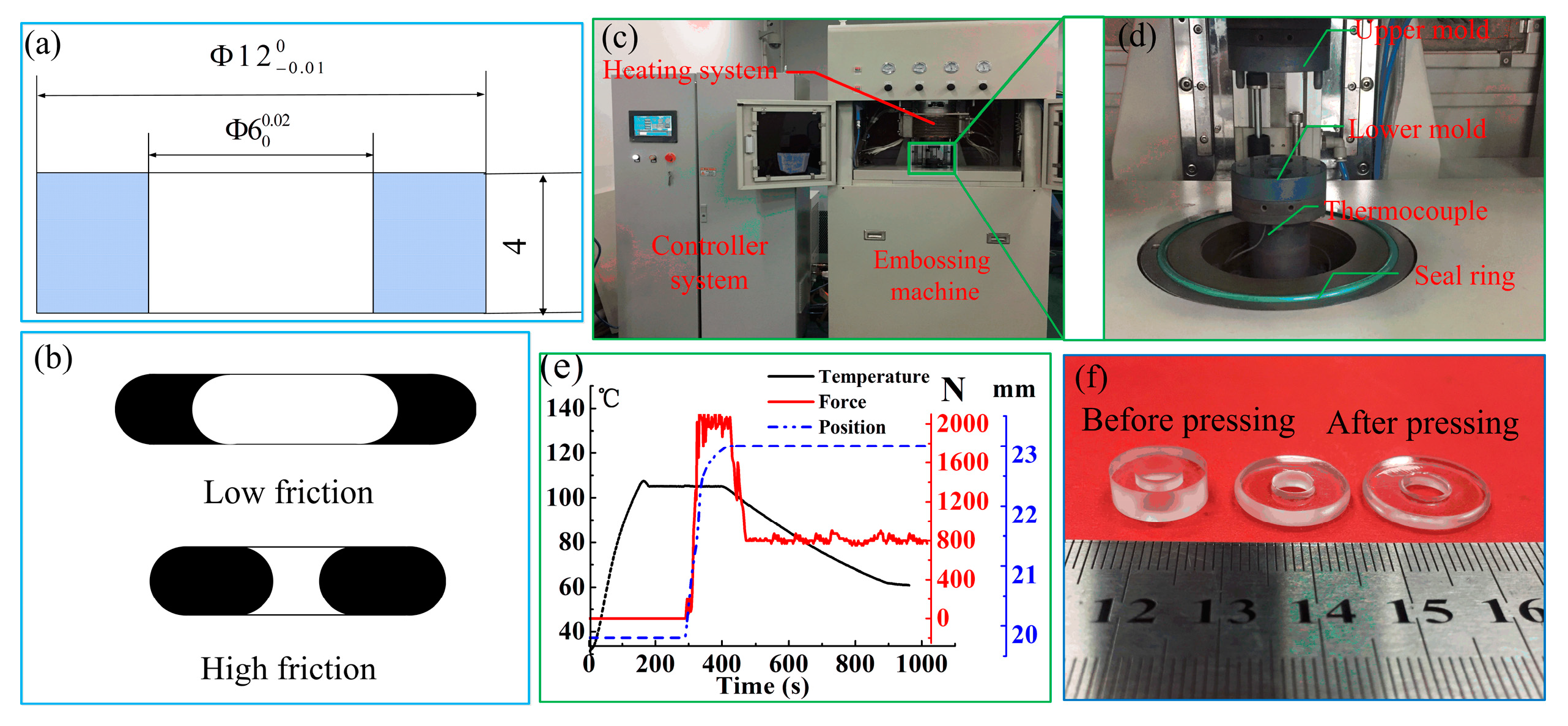
Figure 1a shows that the PMMA rings were fabricated with an internal diameter (ID) of 6 mm, an outer diameter (OD) of 12 mm, and a height (H) of 4 mm, which is a standard ring ratio of OD:ID:H = 6:3:2. Figure 1b shows that effect of friction magnitude on the PMMA deformation during the ring compression test. The high friction force leads to an inward flow of the PMMA material when a ring is compressed between flat molds. On the contrary, the inner diameter of ring increases when the friction is low. Therefore, we can obtain the friction coefficient between PMMA and mold by this relationship. The surface roughness of the PMMA ring is between Ra 5 to 7 nm (see Figure 1f). Our team conducted a series of ring compression tests on SZU’s PGMM30 (see Figure 1c,d). The heating chamber provided a vacuum, or Nitrogen environment, for the embossing process. The upper mold remained stationary, while the lower mold was driven upward and downward by an AC servomotor system. The load of the system was monitored by a load cell with a resolution of 1 N. During the embossing stage, the lower mold position was recorded by a position sensor with a resolution of 1 μm. To obtain the relationship between friction coefficient and temperature, a series of rings were compressed under different temperatures (90, 105, 120, 135, and 150 °C). Figure 1e shows the history of temperature, force, and position time. Figure 1f shows the compressed PMMA ring under different temperatures.
2.3. The Manufacture of the Micro-EDM Mold Insert
The copper micro-electrode, of which diameter was 250 µm, was used in micro-EDM to process micro-hole arrays. Figure 2a shows the schematic of the micro-EDM. Figure 2b shows the image of the electrical discharge machine (Sodick, Japan). The processing parameters of micro-EDM consist of voltage, pulse frequency, pulse width, and pulse interval [37,38]. Through adjusting the processing parameters, micro-EDM can effectively fabricate micro-hole arrays. In the micro-EDM process, the voltage was set as 100 V, applied to the material. The workpiece material was a SKD-11 mold tool. The pulse frequency was set to 0.2 MHz. The pulse width and pulse internal was set to 500 and 400 nanoseconds, respectively. Figure 2c,d show the experimental results. From the local SEM image of micro-hole array, the diameter of micro-holes is consistent. It is noteworthy that the side wall of micro-holes is not smooth. Therefore, the micro-hole array needs to be polished being applying in embossing. The micro-electrodes always have wear during micro-EDM process, which results in the inconsistent depth of micro-holes [37]. In the study, the fabrication micro-hole was blind. The wear of micro-electrodes affected the depth accuracy of micro-holes, which should be avoided. Thus, the depth of micro-holes was ensured by position compensation. The diameter and depth of each hole was around 320 and 300 µm, respectively.
2.4. Fabrication of Micro-Lens Array
The micro-embossing process includes presetting, heating, embossing, cooling, and demolding (see Figure 3). The processing parameters, such as embossing temperature, embossing pressure, keeping pressure, embossing time, and cooling velocity, have great influence on the friction characteristic, deformation behavior, and replication quality of hot embossing micro structures.
At the beginning of embossing, the chamber of the embossing apparatus was vacuumed using a vacuum pump. Then, the mold and the PMMA material were heated to a temperature between glass transition and melting point, and soaked for about 100 s to make temperature uniformly distributed. Furthermore, the lower mold was moved by the servomotor drive, controlled by load cell and position sensor. The embossing pressure was in the range of 200–800 N. Finally, nitrogen flowed through the embossing chamber to cool the molds and substrate to a certain temperature. When the mold cooled to room temperature, the PMMA substrates were demolding.
The main influencing factors, including embossing temperature, embossing pressure, and holding time, were performed with sensitivity analysis by investigating orthogonal experiment. In our case, the orthogonal experiment was composed of three factors with three levels, namely embossing temperature, embossing force, and holding time (see Table 2).
3. Finite Element Model
Between glass transition and melting temperature, PMMA shows as viscoelastic behaviors. In this study, the viscoelastic material was treated as a general Maxwell model. The temperature dependence of PMMA material can be treated as a Thermally Rhetorically Simplicity (TRS) model by the Williams-Landel-Ferry (WLF) equation [39]. C1 and C2 are the WLF equation constants that can be fitted.
The response of PMMA material to the continuous stress history can be expressed by the general Maxwell model
where t is the current time; the past time; are the weigh factors; and G is the modulus of material.
Stress relaxation at different temperatures can be expressed by WLF Equation [39]
where Tref is the reference temperature and C1 and C2 are the WLF equation constants that can be fitted. As for the PMMA material, C1 and C2 can be taken as 17.4 and 51.6, respectively [40]. The mechanical properties were obtained from the literature [41,42].
Figure 4 shows the initial geometry of the model, including the PMMA, the upper mold, lower mold, and mold core. In order to reduce the computation, one fourth of the coupled thermal-displacement model was developed in the software. The PMMA was modeled as linear viscoelastic material, and the molds were treated as elastic material. Two master-slave types of contact interaction pairs were established when the interface behaviors were treated as hard contact and coulomb friction model with penalty formulation. The PMMA/mold interface friction coefficient was obtained from the ring compression tests. The surfaces of upper and lower mold were defined as the master surface. The vertical displacement of the upper mold was fixed with the horizontal displacement to keep free. The heating mechanism in the PMMA embossing refers to gap heat conductance and radiation.
4. Results and Discussion
4.1. Friction Coefficient between PMMA and Mold
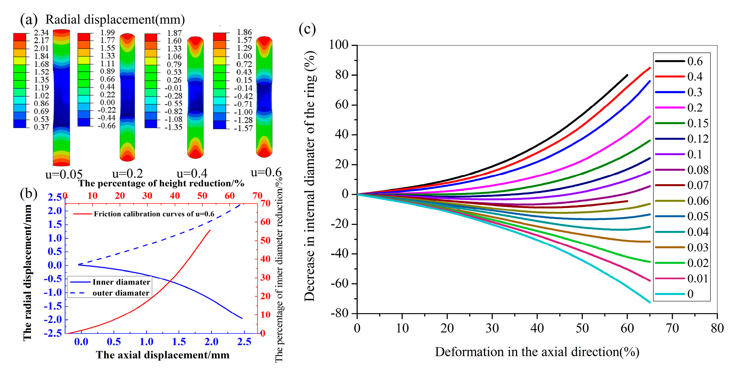
Friction at the mold/PMMA interface affects the flow ability, molding force, shape of molded PMMA, and mold life in forming process. To understand the deformation behaviors of PMMA, numerical simulation is an effective method to predict the shape of molded PMMA. Figure 5a shows the simulation results of the PMMA ring for different interface friction coefficients, assuming the PMMA ring was pressed to the same vertical displacement. If the interfacial friction was low, the deformation configuration of the PMMA material was radially outward. On the contrary, the inner diameter reduced when the external diameter increased with the increased friction coefficient. Figure 5b shows the change curve of the ring deformation during the pressing stage. Figure 5c shows the numerical friction calibration curves by extracting the dimensional changes of the PMMA ring.
To investigate the influence of temperature, the forming temperature of the PMMA ring was set at 90, 105, 120, 135 and 150 °C, respectively. Figure 6a shows the deformation dimension of the pressed rings at the range of 90–150 °C. Interesting changes were that the inner diameter of PMMA ring largened as the temperature rose, and the outer diameter was slightly bulged. Therefore, we obtained the friction condition by observing the dimensional changes of the inner diameter. The inner diameter and height of the ring after cooling were measured by digital Vernier caliper. Table 3 shows the experimental results of the ring compression test. To reduce the size error, each dimension was measured ten times in each different position, with the average taken. Figure 6b shows the numerical calibration curves and measured data points. The friction coefficient at the PMMA/mold was obtained by comparing the friction curves and experimental data. In the range of 90–150 °C, the friction coefficient decreased with the increasing pressing temperature. This was because the deformation resistance gradually reduced by raising the temperature.
4.2. Fabrication of Micro-Lens Array
The height ratios of the micro-lens array change with different processing parameters. It is worth mentioning that the profile of micro-lens array can be replicated randomly by controlling the embossing conditions. The three processing parameters had significant effects on the deformation of the micro-lens array. The results indicated that the flow behaviors of PMMA were much better with the increase of embossing temperature. In addition, the increasing holding pressure and time can reduce the recovery deformation of micro-lens array. The height ratios of micro-lens array became larger as the embossing force rose.
Figure 7 shows the embossed PMMA microstructure under different processing parameters. The aspect ratios of the microstructure changed with different processing parameters. Much like the profile of micro-lens array, the profile of microstructure can also be replicated randomly by controlling the embossing conditions. With the increase of temperature, the depth of the replicated structures increased, and their recovery deformation decreased. The defects occurred on the edge of the microstructures, due to the mold quality, because the edge of mold machined by EDM appeared with some defects affecting the replication quality. In the future studies, the problem of fabrication quality will be solved by polishing or coating.
The ContourGT-X 3D Optical Profiler (Bruker, Germany) was used to observe the surface morphology and profile shape. Figure 8 shows the measurement results of different embossing processing parameters, and the 3D profile and shape of the formed micro-lens array (with diameter ≈ 300 µm, and height ≈ 10 µm) corresponding to Figure 7a. Figure 8b shows the profile shape of the micro-lens array (with diameter ≈ 300 µm, and height ≈ 33 µm) by filtering. It can be concluded that embossing temperature and force are the important factors on the contactless hot embossing process.
The stress inside the microstructure affected the optical quality of the embossed micro-lens because of temperature gradient during cooling. The simulation can be used to investigate the evolution mechanism of residual stress during hot embossing. Figure 9 shows the Von Mise stress and friction shear stress of the micro-lens array from FE simulation. The maximum stress focused on the edge of the microstructure, and the lowest stress took place around the center of microstructure. The deformation characteristic of the PMMA during hot embossing is dependent on temperature. The stress concentrated in the contact edge region of the lens, during thermal loading process, which led to large plastic deformation in the region. Stress concentration and shear flow led to the defects and strain hardening of the micro-lens, affecting the optical quality. The friction coefficient had a great effect on the shear deformation. To reduce the stress concentration and shear stress, we increased the temperature of mold in the certain range.
4.3. Micro-Optics of Micro-Lens Array
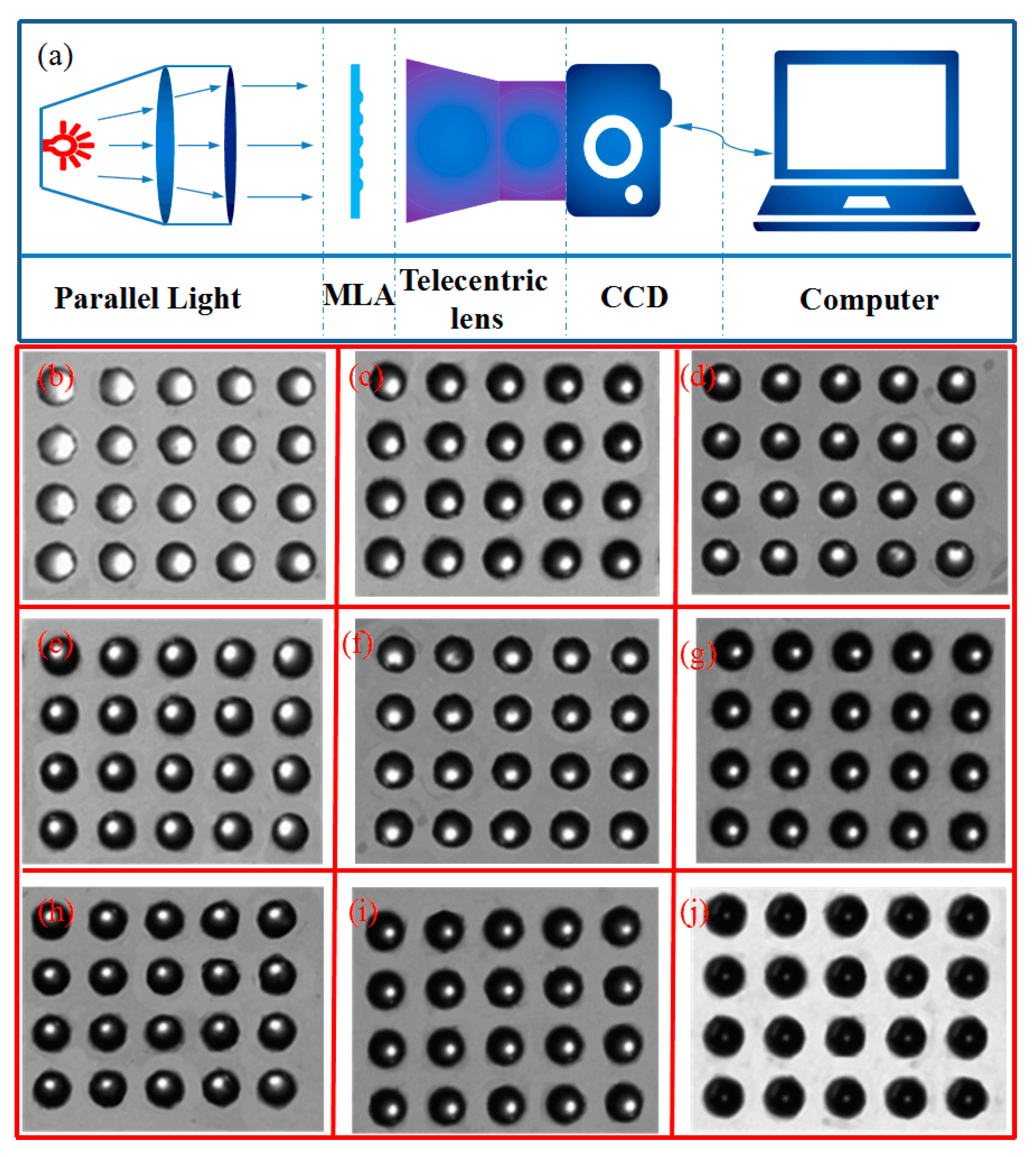
The optical quality of the micro-lens array was the most important parameter. To verify the imaging performance of the micro-lens array, it can be detected by optical measurement system. Figure 10a shows the schematic diagrams of the system. The experiment system consisted of a charge-coupled device (CCD) camera, workbench, directional light source, and computer system. The system had the advantage of convenience and rapid response. Through the projection information, we can estimate the imaging quality.
Figure 10b–j shows the focused light spots of the embossed micro-lens array corresponding to micro-lens array of Figure 7. The light spots of the micro-lens array had a great difference in the same projection position. From the imaging performance of the micro-lens array, the processing parameters had a great influence on the profile of the lens array. The light spots are non-uniform due to the non-uniformity of the lens shape. In the embossing process, the deformation of the PMMA material had a recovery stage, which was related to the temperature and pressure. When the embossing temperature is 105 °C with embossing force of 200 N and holding time of 120 s, the micro-lens endured larger recovery deformation than that of other processing parameters. Large recovery led to irregular deformations if the process had no intervention. An apparent optical imaging difference can be observed among these micro-lenses under different processing parameters. The temperature and the embossing force were the two crucial parameters affecting the fabrication of micro-lens array.
5. Conclusions
This work reported the embossed micro-lens arrays based on micro-EDM micro-hole array molds. The ring compression test indicated that in the viscous region, the friction force between PMMA and mold decreased as temperature rose. The recovery occurred in the cooling stage without loading, which affected the replication precision. The embossing temperature and force affected deformation and surface morphology of the embossed micro-lens array. The results of this work indicated that the deformation behaviors can be used to fabricate different local lengths of micro-lens. Contactless embossing on the micro-EDM molds was a flexible method with low cost for fabrication of micro-structures arrays.
Author Contributions
Conceptualization, F.G., G.X. and K.L.; Methodology, F.G., K.L. and X.H.; Software, K.L.; Writing-original Draft Preparation, K.L. and Z.X.; Funding Acquisition, F.G.
Funding
The authors gratefully acknowledge the financial support of the Natural Science Foundation of Guangdong Province (2018A030313466) and the Shenzhen Science and Technology Innovation Commission (SGLH20150213170331329).
Acknowledgments
The author would like to appreciate the colleagues for their help to improve the paper.
Conflicts of Interest
The authors declare no conflict of interest.
References
- Kuang, D.; Zhang, X.; Gui, M.; Fang, Z. Hexagonal microlens array fabricated by direct laser writing and inductively coupled plasma etching on organic light emitting devices to enhance the outcoupling efficiency. Appl. Opt. 2009, 48, 974. [Google Scholar] [CrossRef] [PubMed]
- Lim, C.S.; Hong, M.H.; Kumar, A.S.; Rahman, M.; Liu, X.D. Fabrication of concave micro lens array using laser patterning and isotropic etching. Int. J. Mach. Tool Manuf. 2006, 46, 552–558. [Google Scholar] [CrossRef]
- Mccall, B.; Descour, M.; Tkaczyk, T. Fabrication of plastic microlens arrays for array microscopy by diamond milling techniques. Opt. Eng. 2010, 49, 730. [Google Scholar] [CrossRef] [PubMed]
- Wu, H.; Odom, T.W.; Whitesides, G.M. Reduction photolithography using microlens arrays: Applications in gray scale photolithography. Anul. Chem. 2002, 74, 3267–3273. [Google Scholar] [CrossRef]
- Luo, C.W.; Chiang, Y.C.; Cheng, H.C.; Wu, C.Z.; Huang, C.F.; Wu, C.W.; Shen, Y.K.; Lin, Y. A novel and rapid fabrication for microlens arrays using microinjection molding. Poly. Eng. Sci. 2011, 51, 391–402. [Google Scholar] [CrossRef]
- Chang, C.Y.; Yang, S.Y.; Huang, L.S.; Chang, J.H. Fabrication of plastic microlens array using gas-assisted micro-hot-embossing with a silicon mold. Infrared Phys. Technol. 2006, 48, 163–173. [Google Scholar] [CrossRef]
- Albero, J.; Perrin, S.; Bargiel, S.; Passilly, N.; Baranski, M.; Gauthier-Manuel, L.; Bernard, F.; Lullin, J.; Froehly, L.; Krauter, J.; et al. Dense arrays of millimeter-sized glass lenses fabricated at wafer-level. Opt. Express 2015, 23, 11702–11712. [Google Scholar] [CrossRef] [PubMed]
- Ong, N.S.; Koh, Y.H.; Fu, Y.Q. Microlens array produced using hot embossing process. Microelectron. Eng. 2002, 60, 365–379. [Google Scholar] [CrossRef]
- Chang, C.Y.; Yang, S.Y.; Chu, M.H. Rapid fabrication of ultraviolet-cured polymer microlens arrays by soft roller stamping process. Microelectron. Eng. 2007, 84, 355–361. [Google Scholar] [CrossRef]
- Kunnavakkam, M.V.; Houlihan, F.M.; Schlax, M.; Liddle, J.A.; Kolodner, P.; Nalamasu, O.; Rogers, J.A. Low-cost, low-loss microlens arrays fabricated by soft-lithography replication process. Appl. Phys. Lett. 2003, 82, 1152–1154. [Google Scholar] [CrossRef]
- Lin, C.R.; Chen, R.H.; Hung, C. Preventing non-uniform shrinkage in open-die hot embossing of PMMA microstructures. J. Mater. Process. Technol. 2003, 140, 173–178. [Google Scholar] [CrossRef]
- Chang, C.Y.; Yu, C.H. A basic experimental study of ultrasonic assisted hot embossing process for rapid fabrication of microlens arrays. J. Micromech. Microeng. 2015, 25. [Google Scholar] [CrossRef]
- Liu, Y.; Zhang, P.; Deng, Y.; Hao, P.; Fan, J.; Chi, M.; Wu, Y. Polymeric microlens array fabricated with PDMS mold-based hot embossing. J. Micromech. Microeng. 2014, 24, 95028. [Google Scholar] [CrossRef]
- Chang, C.Y.; Yang, S.Y.; Huang, L.S.; Hsieh, K.H. Fabrication of polymer microlens arrays using capillary forming with a soft mold of micro-holes array and UV-curable polymer. Opt. Express 2006, 14, 6253–6258. [Google Scholar] [CrossRef] [PubMed]
- Hu, C.N.; Hsieh, H.T.; Su, G.D.J. Fabrication of microlens arrays by a rolling process with soft polydimethylsiloxane molds. J. Micromech. Microeng. 2011, 21, 65013. [Google Scholar] [CrossRef]
- Kim, M.; Moon, B.U.; Hidrovo, C.H. Enhancement of the thermo-mechanical properties of PDMS molds for the hot embossing of PMMA microfluidic devices. J. Micromech. Microeng. 2013, 23, 95024. [Google Scholar] [CrossRef]
- Goral, V.N.; Hsieh, Y.C.; Petzold, O.N.; Faris, R.A.; Yuen, P.K. Hot embossing of plastic microfluidic devices using poly(dimethylsiloxane) molds. J. Micromech. Microeng. 2010, 21, 17002–17009. [Google Scholar] [CrossRef]
- Pan, L.W.; Shen, X.; Lin, L. Microplastic lens array fabricated by a hot intrusion process. J. Micoelectromech. Syst. 2004, 13, 1063–1071. [Google Scholar] [CrossRef]
- Dong, S.K.; Lee, H.S.; Lee, B.K.; Sang, S.Y.; Tai, H.K.; Lee, S.S. Replications and analysis of microlens array fabricated by a modified LIGA process. Poly. Eng. Sci. 2006, 46, 416–425. [Google Scholar] [CrossRef]
- Lan, S.; Lee, H.J.; Kim, E.; Ni, J.; Lee, S.H.; Lai, X.; Song, J.H.; Lee, N.K.; Lee, M.G. A parameter study on the micro hot-embossing process of glassy polymer for pattern replication. Microelectron Eng. 2009, 86, 2369–2374. [Google Scholar] [CrossRef]
- Youn, S.W.; Okuyama, C.; Takahashi, M.; Maeda, R. A study on fabrication of silicon mold for polymer hot-embossing using focused ion beam milling. J Mater. Process. Technol. 2008, 201, 548–553. [Google Scholar] [CrossRef]
- Deng, Y.; Yi, P.; Peng, L.; Lai, X.; Lin, Z. Experimental investigation on the large-area fabrication of micro-pyramid arrays by roll-to-roll hot embossing on PVC film. J. Micromech. Microeng. 2014, 24, 45023–45034. [Google Scholar] [CrossRef]
- Yeo, L.P.; Ng, S.H.; Wang, Z.F.; Xia, H.M.; Wang, Z.P.; Thang, V.S.; Zhong, Z.W.; De Rooij, N.F. Investigation of hot roller embossing for microfluidic devices. J. Micromech. Microeng. 2009, 20, 837–854. [Google Scholar] [CrossRef]
- Schulze, J.; Ehrfeld, W.; Loewe, H.; Michel, A.; Picard, A. Contactless embossing of microlenses: A new technology for manufacturing refractive microlenses. Proc. SPIE 1997, 89–98. [Google Scholar] [CrossRef]
- Schulze, J.; Ehrfeld, W.; Mueller, H.; Picard, A. Compact self-aligning assemblies with refractive microlens arrays made by contactless embossing. Proc. SPIE 1998. [Google Scholar] [CrossRef]
- Xie, D.; Chang, X.; Shu, X.; Wang, Y.; Ding, H.; Liu, Y. Rapid fabrication of thermoplastic polymer refractive microlens array using contactless hot embossing technology. Opt. Express 2015, 23, 5154–5166. [Google Scholar] [CrossRef] [PubMed]
- Moore, S.; Gomez, J.; Lek, D.; You, B.H.; Kim, N.; Song, I.H. Experimental study of polymer microlens fabrication using partial-filling hot embossing technique. Microelectron. Eng. 2016, 162, 57–62. [Google Scholar] [CrossRef]
- Ho, K.H.; Newman, S.T. State of the art electrical discharge machining (EDM). Int. J. Mach. Tool Manuf. 2003, 43, 1287–1300. [Google Scholar] [CrossRef]
- Abbas, N.M.; Solomon, D.G.; Bahari, M.F. A review on current research trends in electrical discharge machining (EDM). Int. J. Mach. Tool Manuf. 2006, 47, 1214–1228. [Google Scholar] [CrossRef]
- Worgull, M.; Xe, H.; Tu, J.F.; Kabanemi, K.K.; Heckele, M. Hot embossing of microstructures: Characterization of friction during demolding. Microsyst. Technol. 2008, 14, 767–773. [Google Scholar] [CrossRef]
- Guo, Y.; Liu, G.; Zhu, X.; Tian, Y. Analysis of the demolding forces during hot embossing. Microsyst. Technol. 2007, 13, 411–415. [Google Scholar] [CrossRef]
- Zhao, F.; Li, H.; Ji, L.; Wang, Y.; Zhou, H.; Chen, J. Ti-DLC films with superior friction performance. Diam. Relat. Mater. 2010, 19, 342–349. [Google Scholar] [CrossRef]
- Male, A.T.; Depierre, V. The Validity of Mathematical Solutions for Determining Friction from the Ring Compression Test. J. Tribol. 1970, 92, 389. [Google Scholar] [CrossRef]
- Yao, Z.; Mei, D.; Chen, Z. A Friction Evaluation Method Based on Barrel Compression Test. Tribol. Lett. 2013, 51, 525–535. [Google Scholar] [CrossRef]
- Zhu, Y.; Zeng, W.; Ma, X.; Tai, Q.; Li, Z.; Li, X. Determination of the friction factor of Ti-6Al-4V titanium alloy in hot forging by means of ring-compression test using FEM. Tribol. Int. 2011, 44, 2074–2080. [Google Scholar] [CrossRef]
- Sarhadi, A.; Hattel, J.H.; Hansen, H.N. Evaluation of the viscoelastic behaviour and glass/mold interface friction coefficient in the wafer based precision glass molding. J. Mater. Process. Technol. 2014, 214, 1427–1435. [Google Scholar] [CrossRef]
- Xu, B.; Wu, X.Y.; Lei, J.G.; Cheng, R.; Ruan, S.C.; Wang, Z.L. Laminated fabrication of 3D queue micro-electrode and its application in micro-EDM. Int. J. Adv. Manuf. Technol. 2015, 80, 1701–1711. [Google Scholar] [CrossRef]
- Xu, B.; Wu, X.Y.; Lei, J.G.; Zhao, H.; Liang, X.; Cheng, R.; Guo, D.J. Elimination of 3D micro-electrode’s step effect and applying it in micro-EDM. Int. J. Adv. Manuf. Technol. 2018, 96, 1–10. [Google Scholar] [CrossRef]
- Williams, D.; Landel, R.F.; Ferry, J.D. The temperature dependance of relaxation mechanisms in amorphous polymers and other glass form liquids. J. Am. Chem. Soc. 1955, 77, 3701–3707. [Google Scholar] [CrossRef]
- Cheng, E.; Yin, Z.; Zou, H.; Jurčíček, P. Experimental and numerical study on deformation behavior of polyethylene terephthalate two-dimensional nanochannels during hot embossing process. J. Micromech. Microeng. 2013, 24, 5004. [Google Scholar] [CrossRef]
- Omar, F.; Brousseau, E.; Elkaseer, A.; Kolew, A.; Prokopovich, P.; Dimov, S. Development and experimental validation of an analytical model to predict the demolding force in hot embossing. J. Micromech. Microeng. 2014, 24, 55007. [Google Scholar] [CrossRef]
- He, Y.; Fu, J.Z.; Chen, Z.C. Research on optimization of the hot embossing process. J. Micromech. Microeng. 2007, 17, 2420. [Google Scholar] [CrossRef]
Figure 1.
(a) Dimension of the polymethyl methacrylate (PMMA) rings; (b) effect of friction magnitude with PMMA deformation during ring compression test; (c) Shenzhen University’s precision glass molding machine (SZU’s PGMM30); (d) mold assembly; (e) time history of the force, temperature, and position; (f) before and after pressing of the PMMA ring.

Figure 2.
(a) The schematic of the micro-electric discharge machining (EDM); (b) picture of the experiment apparatus (AP1L); (c) the SEM diagram of the micro-hole array of mold; (d) the dimensions and layout of the micro-holes array.
Figure 2.
(a) The schematic of the micro-electric discharge machining (EDM); (b) picture of the experiment apparatus (AP1L); (c) the SEM diagram of the micro-hole array of mold; (d) the dimensions and layout of the micro-holes array.

Figure 3.
Schematic of micro-embossing process using electrical discharge machining (EDM) mold.

Figure 4.
The initial geometry model used for simulation of the contactless micro-embossing process.
Figure 4.
The initial geometry model used for simulation of the contactless micro-embossing process.

Figure 5.
The simulation results. (a) The PMMA ring compression for different interface friction coefficient; (b) the displacement change of the diameters, and the friction calibration curve obtained from the simulation results; (c) numerical friction calibration curves under different friction coefficient.

Figure 6.
PMMA compression test: (a) The ring after compression under different temperatures; (b) numerical friction calibration curves and experimental data.
Figure 6.
PMMA compression test: (a) The ring after compression under different temperatures; (b) numerical friction calibration curves and experimental data.

Figure 7.
Micro-Embossing PMMA micro-lens array under different processing parameters. (a) 105 °C/200 N/120 s; (b) 105 °C/400 N/180 s; (c) 105 °C/800 N/240 s; (d) 120 °C/200 N/120 s; (e) 120 °C/400 N/240 s; (f) 120 °C/800 N/180 s; (g) 135 °C/200 N/240 s; (h) 135 °C/400 N/180 s; (i) 135 °C/800 N/120 s.

Figure 8.
Profile of micro-lens measured using ContourGT-X 3D Optical Profiler. (a) Forming under conditions of 105 °C/200 N/120 s; (b) forming under conditions of 135 °C/800 N/120 s.
Figure 8.
Profile of micro-lens measured using ContourGT-X 3D Optical Profiler. (a) Forming under conditions of 105 °C/200 N/120 s; (b) forming under conditions of 135 °C/800 N/120 s.

Figure 9.
The stress distribution of micro-lens array. (a) Von Mises stress; (b) friction shear stress.
Figure 9.
The stress distribution of micro-lens array. (a) Von Mises stress; (b) friction shear stress.

Figure 10.
(a) Schematic diagram of the experimental system; (b) the light spots of the micro-lens array from Figure 7a; (c) The light spots of the micro-lens array from Figure 7b; (d) the light spots of the micro-lens array from Figure 7c; (e) the light spots of the micro-lens array from Figure 7d; (f) the light spots of the micro-lens array from Figure 7e; (g) the light spots of the micro-lens array from Figure 7f; (h) The light spots of the micro-lens array from Figure 7f; (i) the light spots of the micro-lens array from Figure 7h; (j) the light spots of the micro-lens array from Figure 7i.


Table 1.
The physical properties of polymethyl methacrylate (PMMA) and SKD-11 mold.
| Property | PMMA | SKD-11 |
|---|---|---|
| Young’s Modulus (GPa) | 2.4 | 210 |
| Poisson ratio | 0.37 | 0.2 |
| Density (kg/m3) | 1185 | 7700 |
| Thermal conductivity (W/m2∙K) | 0.2 | 200 |
| Specific heat (J/kg∙K) | 1466 | 460 |
| Thermal expansion (K−1) | 4.4 × 10⁻⁴ | 11 × 10−6 |
| Glass transition temperature (°C) | 105 | - |
| Melting temperature (°C) | 220 | - |
Table 2.
List of factors, levels for orthogonal design.
| Levels | Factors | ||
|---|---|---|---|
| Embossing Temperature (°C) | Embossing Force (N) | Holding Time (s) | |
| 1 | 105 | 200 | 120 |
| 2 | 120 | 400 | 180 |
| 3 | 135 | 800 | 240 |
Table 3.
The experimental results of the ring compression test.
| No. | Temp./ °C | Force/N | ID/mm | OD/mm | T/mm |
|---|---|---|---|---|---|
| 1 | 90 | 3000 | 5.21 | 13.26 | 3.10 |
| 2 | 90 | 3000 | 4.66 | 13.85 | 2.75 |
| 3 | 90 | 3000 | 2.34 | 14.66 | 3.96 |
| 4 | 105 | 2000 | 5.17 | 13.37 | 3.05 |
| 5 | 105 | 2000 | 4.61 | 14.08 | 2.66 |
| 6 | 105 | 2000 | 3.88 | 14.48 | 2.20 |
| 7 | 120 | 1500 | 5.51 | 14.25 | 2.73 |
| 8 | 120 | 1500 | 5.22 | 15.06 | 2.33 |
| 9 | 120 | 1500 | 3.87 | 16.09 | 1.89 |
| 10 | 135 | 1000 | 5.81 | 14.47 | 2.72 |
| 11 | 135 | 1000 | 5.37 | 15.48 | 2.22 |
| 12 | 135 | 1000 | 5.01 | 17.00 | 1.75 |
| 13 | 150 | 500 | 6.30 | 15.26 | 2.70 |
| 14 | 150 | 500 | 6.06 | 15.78 | 2.15 |
| 15 | 150 | 500 | 5.88 | 17.51 | 1.71 |
© 2018 by the authors. Licensee MDPI, Basel, Switzerland. This article is an open access article distributed under the terms and conditions of the Creative Commons Attribution (CC BY) license (http://creativecommons.org/licenses/by/4.0/).
Share and Cite
MDPI and ACS Style
Li, K.; Xu, G.; Huang, X.; Xie, Z.; Gong, F. Manufacturing of Micro-Lens Array Using Contactless Micro-Embossing with an EDM-Mold. Appl. Sci. 2019, 9, 85. https://doi.org/10.3390/app9010085
AMA Style
Li K, Xu G, Huang X, Xie Z, Gong F. Manufacturing of Micro-Lens Array Using Contactless Micro-Embossing with an EDM-Mold. Applied Sciences. 2019; 9(1):85. https://doi.org/10.3390/app9010085
Chicago/Turabian StyleLi, Kangsen, Gang Xu, Xinfang Huang, Zhiwen Xie, and Feng Gong. 2019. "Manufacturing of Micro-Lens Array Using Contactless Micro-Embossing with an EDM-Mold" Applied Sciences 9, no. 1: 85. https://doi.org/10.3390/app9010085
Note that from the first issue of 2016, this journal uses article numbers instead of page numbers. See further details here.