Optically Transparent Nano-Patterned Antennas: A Review and Future Directions


Department of Electrical Engineering, Pohang University of Science and Technology (POSTECH), Pohang 37673, Korea
*
Author to whom correspondence should be addressed.
Appl. Sci. 2018, 8(6), 901; https://doi.org/10.3390/app8060901
Submission received: 30 April 2018
/
Revised: 16 May 2018
/
Accepted: 18 May 2018
/
Published: 31 May 2018
(This article belongs to the Special Issue Nano-Antennas)
Abstract
:Transparent antennas have been continuously developed for integration with solar cells, vehicular communications, and ultra-high-speed communications such as 5G in recent years. A transparent antenna takes advantage of spatial extensibility more so than all other antennas in terms of wide range of usable area. In addition, the production price of transparent antennas is steadily decreasing due to the development of nano-process technology. This paper reviews published studies of transparent antennas classified by various materials in terms of optical transmittance and electrical, sheet resistance. The transparent electrodes for the transparent antenna are logically classified and the transparent antennas are described according to the characteristics of each electrode. Finally, the contributions transparent antennas can make toward next-generation 5G high-speed communication are discussed.
1. Introduction
As nanotechnology continues to develop rapidly, antennas fabricated by transparent conductive films (TCFs) instead of conventionally used metal, i.e., copper, are being fabricated. As a kind of TCF, nano carbon (graphene, carbon nanotubes), transparent conductive oxides, conductive polymer, and metallic nanostructures (metallic nanowires, thin metal films, and patterned metal-grids) are used to design novel antennas. The idea of a transparent antenna was first proposed in order to overlap the antenna with a solar cell on a limited satellite surface area [1]. Since nanomaterial technology processes have progressed, the development of more sophisticated and better performance nano-patterned transparent antennas has been researched over the last decades.
Transparent antennas that have been sporadically studied using different types of TCFs are analyzed material-analytically in Section 2. In Section 3, we summarize the performance of the published examples of transparent antennas, referring to the figure of merit (FoM) of the TCFs. Finally, the role and promising contribution of the transparent antenna that can be directly integrated within active displays and denoted as Antenna-on-Display (AoD) is discussed.
2. Transparent Antennas: A Review
2.1. Nano Carbon
2.1.1. Graphene
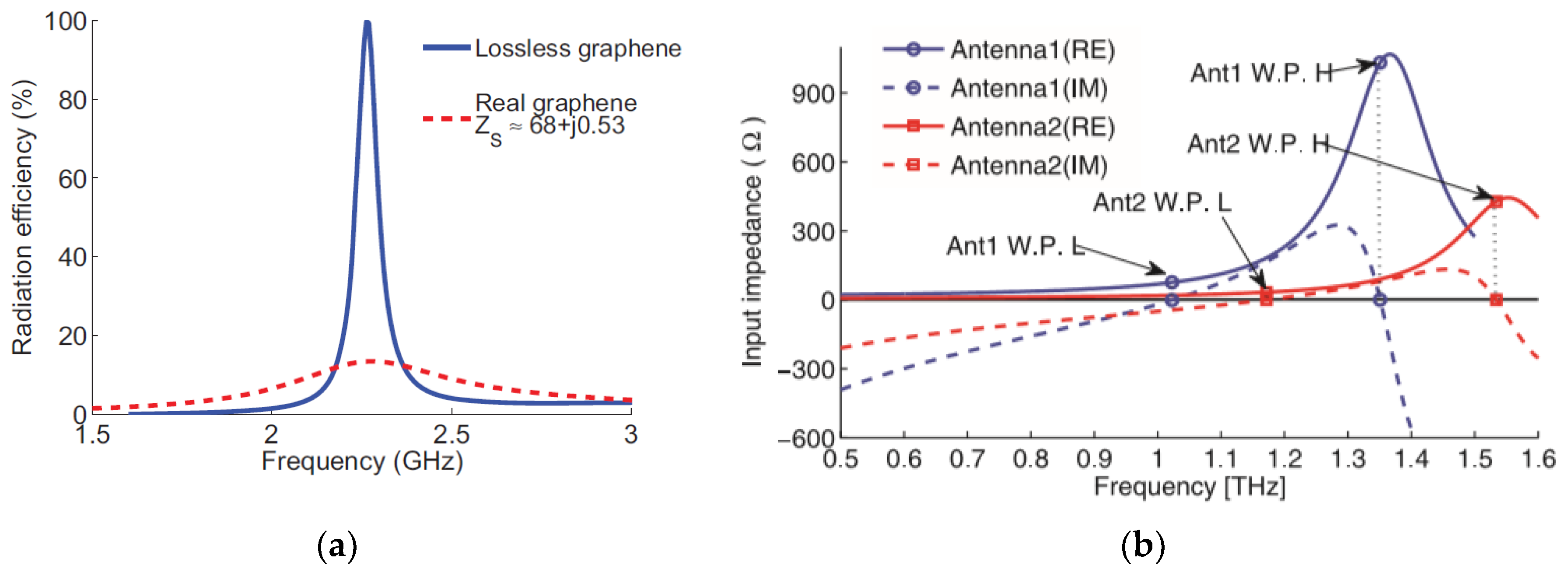
Graphene is one of the carbon isotopes and it has a structure in which carbon atoms gather to form a two-dimensional plane. Each carbon atom forms a hexagonal lattice, with the carbon atoms located at the vertices of the hexagon, called a honeycomb lattice. General methods to obtain graphene thin films include micromechanical exfoliation, epitaxial growth, chemical vapor deposition (CVD), and reduced graphene oxide [2,3]. From an electrical point of view, graphene is a zero-gap semiconductor, or semi-metal, whose complex conductivity nature (frequency-dependent conductivity) allows the propagation of plasmonic modes at THz frequencies [4]. Therefore, a graphene antenna operates at the THz frequency using the negative imaginary conductivity characteristics of graphene, as shown in Figure 1.
In Reference [6,7], graphene-based antennas devised in microwave frequency and THz frequency are investigated. A graphene-based patch antenna resonating at the microwave frequency features a radiation efficiency of 8% in Figure 2a. On the other hand, using plasmonic propagation in the THz frequency, it is confirmed that the antenna efficiency is 60% due to transverse magnetic plasmon surface mode in Figure 2b. Owing to its negative imaginary conductivity, research on tunable devices, frequency selective surface, or reconfigurable antennas using graphene is now being conducted [8,9].
2.1.2. Carbon Nanotubes
Carbon nanotubes (CNTs), discovered in 1991 [10], have been studied for various physical and chemical properties and applications. Types of CNTs include single wall carbon nanotubes (SWCNT), double wall carbon nanotubes (DWCNT), and multi wall carbon nanotubes (MWCNT). SWCNTs are more difficult to synthesize than MWCNT and have high utilization because they have excellent electronic characteristics. The high purity SWCNT required in the field of electronic equipment is currently produced at a small amount at a high cost. MWCNTs have already started to be commercially produced in high volumes and are now used in super capacitors, lithium ion batteries, etc.
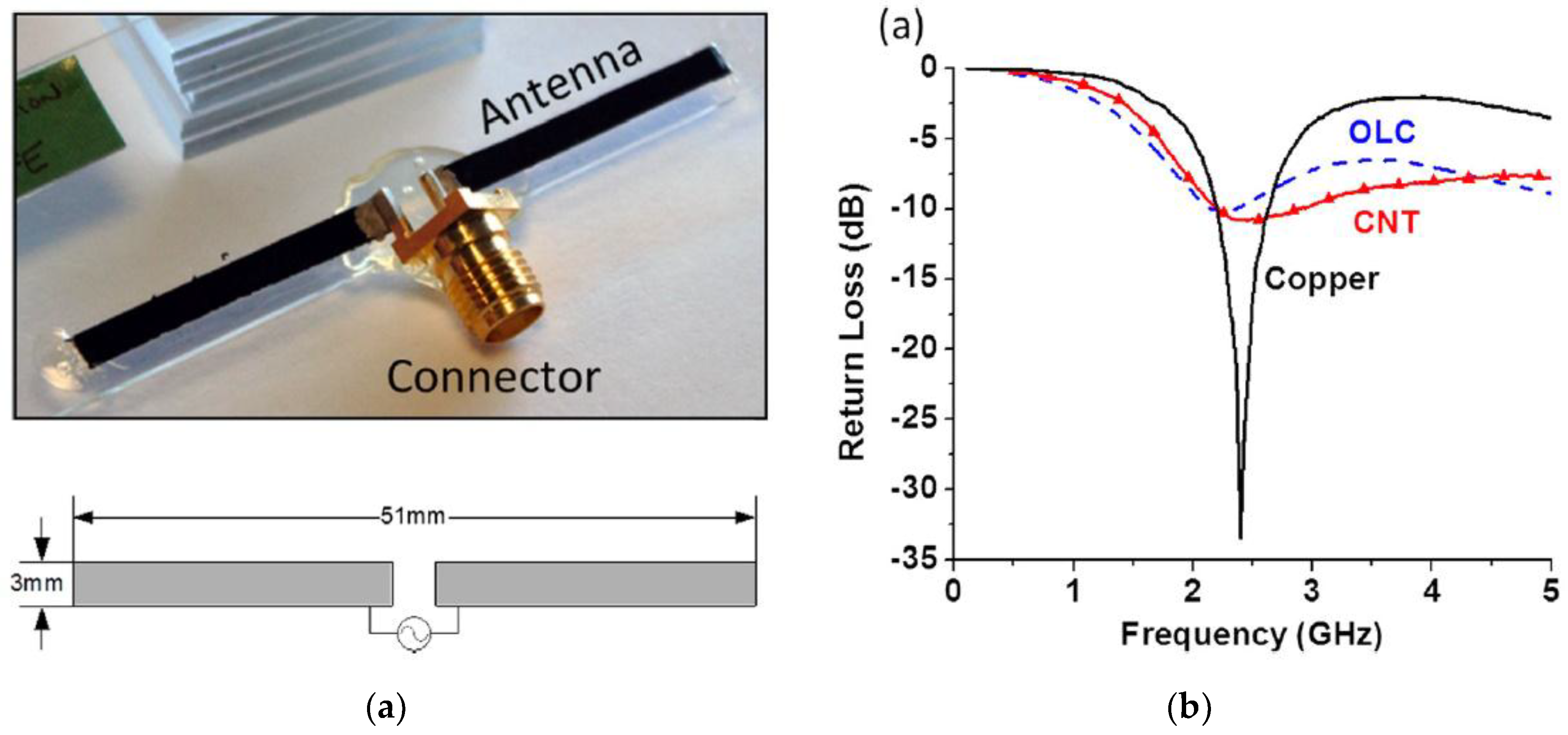
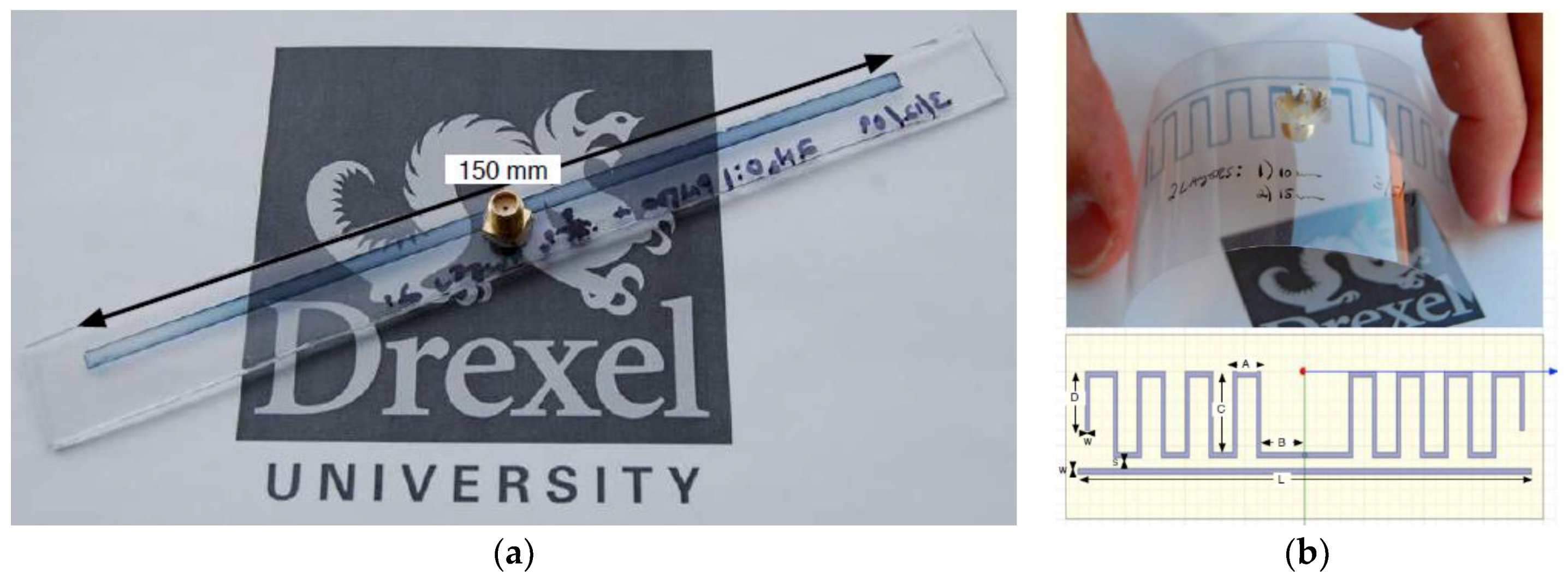
In Reference [11], onion-like carbon (OLC) and MWCNT dipole antennas operating at 2.4 GHz for a wireless local area network (WLAN) such as IEEE 802.11.b/g are studied. The OLC antenna is fabricated with annealing process at 1800 °C for 3 h while the MWCNT antenna is grown on ethylene vapor using an iron catalyst. The sample with 3.5 mm square dimensions features conductivity of 1.5 S/cm and 9.0 S/cm for OLC and MWCNT films, respectively. The dipole antenna is attached to borosilicate glass with a thickness of 1 mm and a relative permittivity of 4.6. As illustrated in Figure 3, while the copper film dipole antenna shows a peak return loss of −30 dB, both the OLC and MWCNT dipole antennas exhibit a peak return loss of below −10 dB. Moreover, both the OLC and MWCNT antennas exhibit peak gains of −1.48 dBi and −2.76 dBi, respectively, while the copper film antenna features a peak gain of 3.5 dBi at 2.4 GHz.
In Reference [12], an MWCNT-based microstrip patch antenna operating at diverse frequencies is proposed. A conductive MWCNT ink-jet printing process is used to pattern patch antennas in two dimensions (10 mm × 10 mm and 20 mm × 20 mm) with three different substrates (RO3210, CCFR4, and TMM4). MWCNT ink features an average DC conductivity of 2.2 × 10⁴ S/m with four probe techniques, and complex relative permittivity is obtained from 6.5−j0.9 to 4.5−j0.1 at a frequency range from 300 kHz to 8.5 GHz. While the MWCNT antenna has low gain compared to a copper-based antenna owing to its lower conductivity, it shows a bandwidth increase compared to the corresponding copper antenna without critical degradation in gain and radiation patterns.
As analyzed above, graphene and CNT classified as nano carbon features a much higher sheet resistance than that required for use as a transparent antenna. Graphene is expected to be more active in studying antenna operation at terahertz frequencies using the plasmonic mode. Most of the CNT film electrodes mass-produced at present show a sheet resistance (Rs) of about 200–500 Ω/sq and an optical transmittance (T) of 80%. So, to use CNT film as an antenna in microwave frequencies, it is necessary to study a composite material composed of two or more materials in order to compensate for the disadvantages while maintaining the advantages of one material [13,14], such as spin coating base graphene/SWCNT (Rs = 280 Ω/sq, T = 90%, FoM = 12.4) [15]. Therefore, the development of transparent antennas using nano carbon is expected to be required for the electrical performance improvement of the aforementioned TCFs.
2.2. Transparents Conductive Oxides
Transparent conductive oxides (TCOs), which are mainly used in the industry, are typically indium tin oxide (ITO) with an Rs of 30 to 80 Ω/sq and a T of 90%. Electron beam (e-beam) deposition is a method that is mainly used in the production of ITO film. E-beam deposition has the advantage of making a uniform thin film and can enable ITO to be easily applied to other materials. ITO fabrication is generally based on a vacuum deposition process, resulting in high uniformity, but also an increase in production cost. In addition, if stable supply and demand is difficult due to the use of indium, which is a rare element, the price volatility is very high. Transparent antennas based on TCO electrodes featuring the above characteristics are further described below. Moreover, TCO-based transparent antennas can be classified as mono-layer or multilayer.
2.2.1. Mono-Layer
In Reference [16], solar transparent patch antennas operating at 28 GHz, which combine function of antenna and solar cell, is presented using TCO films. Transparent antennas help to reduce the shadowing region of the antenna to ensure maximum efficiency of the solar cell. As an antenna part, the rectangular microstrip patch antenna designed with a solar cell is illustrated in Figure 4a. Four types of TCO films (ITO, fluorine-doped tin oxide (FTO), silver-coated polyester films (AgHT-4, AgHT-8)) were used with a glass substrate, which has a dielectric constant of 4.82 and a thickness of 1.1 mm. The sheet resistances of the four TCO films (ITO, FTO, AgHT-4, AgHT-8) are 10, 24, 4.5, and 8 Ω/sq, respectively. The TCO-based transparent antennas show a wide bandwidth property since they used a thicker glass substrate compared to the RT5880 substrate of copper film, which has a dielectric constant of 2.2 and a thickness of 0.254 mm. Also, FTO provides the highest bandwidth while ITO gives the best performance of return loss.
In Reference [17], ITO- and FTO-based transparent U-shape patch antennas that operate at 750 GHz are analyzed. The ITO (t = 400 nm, σ = 2.88 × 10⁵ S/m), FTO (t = 400 nm, σ = 1.67 × 10⁵ S/m), and reference thin copper (t = 400 nm, σ = 5 × 10⁶ S/m) are fabricated on a transparent polyimide substrate, and the optical transmittance of ITO and FTO is greater than 80%. The thickness, relative permittivity, and loss tangent of the transparent substrate are 20 μm, 3.5, and 0.008, respectively. The bandwidths of the ITO and FTO antennas are 9.54% and 11.49%, which are both is higher than the 3.86% of the reference copper antenna, shown in Figure 4b. The peak radiation efficiencies of the ITO, FTO, and reference antennas are 49.45%, 43.22%, and 79.47%.
2.2.2. Multilayer
In Reference [18], the electrical properties of a multilayer ITO film consisting of ITO/Cu/ITO with a maximum optical transmittance of 61% are investigated to validate the feasibility at the ultrahigh frequency (UHF) band. A transparent monopole antenna is printed on a glass substrate with an ITO/Cu/ITO film, featuring an Rs of 4.7 Ω/sq with an 85- (ITO), 13- (Cu), and 85-nm (ITO) thickness. The glass substrate is Corning glass with a relative permittivity of 5.7 and a loss tangent of 0.0002. The transparent monopole antenna operating at the UHF band (500 to 1300 MHz) is discussed. The ITO/Cu/ITO films feature a theoretical gain of −1.96 dBi, while the gain of the ITO film is −4.10 dBi.
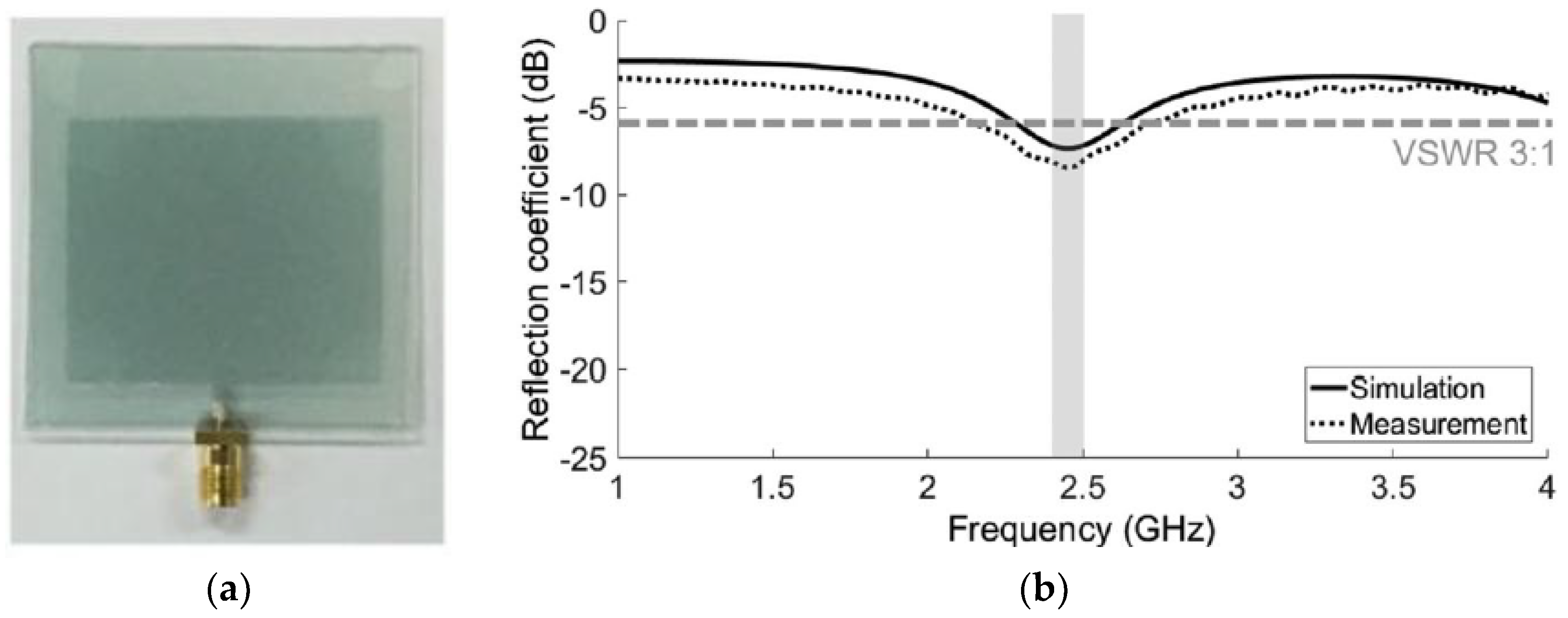
Meanwhile, since ITO has a fragile characteristic at room temperature, other representations of ITO such as Indium Zinc Tin Oxide (IZTO) have been investigated to overcome the inherent weakness of ITO [19]. In Reference [20], the feasibility of a multilayer film-based transparent patch antenna with IZTO is studied at a Wi-Fi service band at 2.45 GHz, as depicted in Figure 5a. The IZTO/Ag/IZTO multilayer film features a sheet resistance of 2.52 Ω/sq and an optical transmittance of above 80%. These antennas used the transparent acryl substrate with a multilayer film with a 100-nm thickness. To evaluate the performance, the reflection coefficient of the multilayer film patch antenna is retrieved in Figure 5b. The multilayer film patch antenna features a peak gain of −4.23 dBi with an efficiency of 7.76%.
2.3. Conductive Polymer
Since the discovery of the conductive polymer polyacetylene in 1977 [21], the study of conductive polymers has been continuously performed. Conductive polymer has a structure in which the main chain is a repeating form of a double bond, which is a structure of an unsaturated hydrocarbon. It is also a form of a single bond, such as in a saturated hydrocarbon structure, and is referred to as a π-conjugated polymer. When the π-conjugated form is present in the polymer skeleton, the electron density is uniform due to doping. Also, electrical conduction occurs. Currently, the most actively studied conductive polymer is poly(3,4-ethylenedioxythiophene): PSS (polystyrene sulfonate), which is a thiophene-based polymer.
In Reference [22], an optically transparent conductive polymer dipole antenna operating at 900 MHz is designed for radio frequency identification (RFID) applications, as illustrated in Figure 6a. An addition of 10% dimethyl sulfoxide (DMSO) is made to the conductive polymer, Clevios PH500 PEDOT-PSS (σ = 300 S/m), to increase the conductivity by 5 × 10³ S/m. The modified conductive polymer (thickness: t = 250 nm) is fabricated on polyethylene terephthalate (PET) (with a thickness of 0.5 mm and a relative permittivity of 3.8) with screen printing and ink-jet printer methods. The optical transmittance of the antenna is between 40% and 70% at different optical wavelengths. The reference dipole copper antenna (σ = 5.8 × 10⁷ S/m) features 2.5 dB and 8 dB higher gain than the screen-printed conductive polymer and ink-jet-printed conductive polymer antennas, respectively. The meandered dipole copper antenna has a 6 dB higher gain than the screen-printed conductive polymer meander antenna in Figure 6b.
In Reference [23], a microstrip-fed proximity-coupled conductive polymer patch antenna resonating at 10 GHz is designed. A polyaniline (Pani) film featuring a conductivity, relative permittivity, and thickness of 6 × 10³ S/m, 6000, and 100 μm is fabricated on alumina using a screen printing technique. The fabricated Pani antenna has a 2.08 dB lower gain than the reference copper antenna due to the many orders of magnitude difference in conductivity.
Conducting polymer has been widely studied for use as a transparent electrode for 40 years. However, conducting polymer has a distinctive color and the disadvantage of lacking atmospheric stability. There is also a limit to the high sheet resistance that nano carbon can suffer. It should be noted that a hybrid process, in which two materials are mixed or multilayered, showed better performance than using one material. Typically, the AgNW/PEDOT:PSS-coated bar shows a sheet resistance of 25 Ω/sq and an optical transmittance of 90% [24].
2.4. Metallic Nanostructure
2.4.1. Nanowire
Silver Nanowires
Silver nanowires (AgNWs) are flexible and conductive materials with very small nanometer (nm) diameters in their cross-section [25]. Due to this characteristic, silver nanowires are attractive as next-generation transparent electrode materials that can replace the indium tin oxide (ITO) in conventional transparent electrodes. In particular, there is a strong interest in silver nanowire transparent electrodes that can be produced in large areas in flexible touch panels and displays. However, the conventional nanowire transparent electrode has a rough surface and a large contact resistance between the nanowires. There is also a limit to the haze phenomenon, which is reflected in the sunlight and shattered. The turbidity and surface roughness of the AgNW can be affected by the dimensions of the AgNW, which is usually from 40 to 100 nm in mean diameter and 1 to 20 μm in mean length [25]. It is possible to realize various Rs (10~100 Ω/sq) by controlling the density of AgNWs. However, as the Rs decreases, the density of AgNWs increases and the optical transmittance T decreases and the turbidity increases [26].
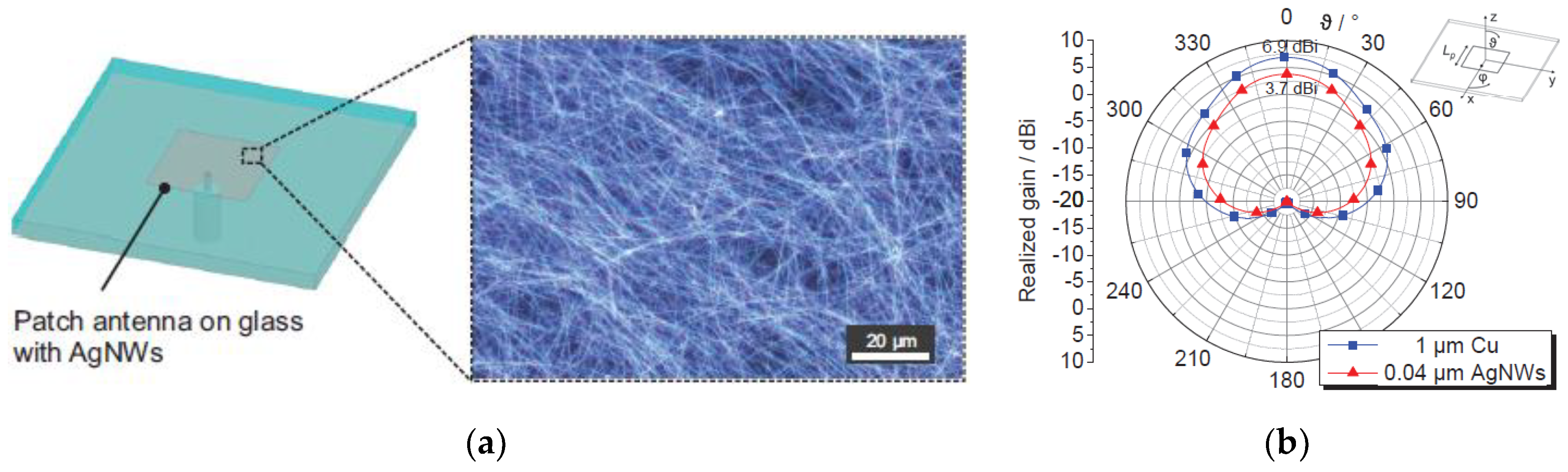
In Reference [27], patch antennas based on optically transparent silver nanowire (AgNW) coatings operating at 24 GHz and 61 GHz are analyzed, as shown in Figure 7a. This AgNW has a mean diameter of 40 nm and a mean length of 15 μm and is coated on glass featuring a thickness of 0.22 mm, relative permittivity of 3.81, and loss tangent of 0.0004 at 24 GHz. The electrical conductivity of AgNW is obtained by comparing the simulation results with the measured insertion loss of coplanar waveguide (CPW), assuming a constant coating thickness of t = 40 nm. The electrical conductivity σ = 7 × 10⁶ S/m is obtained from the comparison. From the result, the sheet resistance of the patch antenna operating at 24 GHz is 0.36 Ω/sq. The patch antennas operating at 24 GHz and 61 GHz have radiation efficiencies of 8.9% and 49.4%, respectively, as shown in Figure 7b, and both have an overall optical transmittance of 51% at 550 nm.
In Reference [28], AgNW patch antennas resonating at 2 GHz for strain sensors are designed. AgNW is embedded in polydimethylsiloxane (PDMS). The final structure features a thickness of 3 mm and an Rs of below 5 Ω/sq. The AgNW patch antenna’s resonant frequency changes with the force applied on it. In Reference [29], a AgNW resonating at 3 GHz patch antenna and a 6 GHz two-element patch array are devised. Similarly, AgNW is embedded in PDMS, which features a relative permittivity of 2.67 to 3 and a loss tangent of 0.01 to 0.05. The conductivity of AgNW is approximately 8.13 × 10⁴ S/cm, and it can be considered as 8.13 × 10⁴ S/cm assuming that the applied strains are relatively small. The radiation efficiency and bandwidth (S11 < −10 dB) of the single antenna and antenna array are 41.83%/88 MHz and 48.8%/330 MHz, respectively. The radiation efficiency deterioration is mainly caused by PDMS rather than AgNW.
Copper Nanowires
Copper nanowires (CuNW) can be coated on various substrates (film, glass, silicon wafer, etc.) by dispersing nanoparticles in solvent and applying wet coating and roll-to-roll coating technology, as compared to existing ITO films. In addition, it has excellent conductivity and flexibility, and is applicable to almost all applications where excellent conductivity and optical transmittance are required, for example, electromagnetic interference (EMI) shielding films, solar cells, transparent electrodes, antennas, and the like. Also, the line spacing between the patterns is so small that it is invisible and usually maintains an interval of 100 to 200 μm.
In Reference [30], a transparent dual-band meandered-monopole antenna with a micro metal mesh conductive film is studied. Using nonconductive glue, the antenna pattern is glued on glass with a 1.09-mm thickness and a relative permittivity of 5.5. The overall dimensions of the fabricated antenna are 40 mm × 40 mm. The micro metal mesh conductive film has a low sheet resistance of 0.05 Ω/sq and a high optical transmittance of above 75%, as given in Figure 8a. The S21 in Figure 8b shows the little effect of mutual coupling between two antennas since S21 is lower than −15 dB at the operating frequency. Moreover, it offers high efficiencies of 43% and 46% and peak gains of 0.74 and 2.30 dBi at 2.44 and 5.5 GHz, which are much higher than those of other materials such as TCOs.
In [31], a transparent 3 dB Branch-Line Coupler based on a micro metal mesh conductive film is investigated, operating at 2.45 GHz. This antenna pattern is printed on a stacked substrate which has PET/glass/PET layers. The thickness of the glass substrate is 2 mm with a dielectric constant of 5.7. Owing to the large thickness (2.25 mm) of the overall substrate, a wide band property is obtained. It can reduce the low sheet resistance to 0.7 Ω/sq, but it has a transmittance of 75% and also yields a return loss of 20.2 dB and an isolation of 23.5 dB.
2.4.2. Ultra-Thin Metal Films
Transparent ultra-thin metal films have been reported as good candidates for transparent electrodes because they are easy to process and feature high conductivity. Metal candidates for ultra-thin metal electrodes are mainly Ag and Cu. Ag is the most commonly used film material because it has the lowest electrical resistance and optical loss in the visible spectrum of known metals [32].
AgHT commercial product, which is widely used, is a silver-coated highly conductive ITO film and the value 4 at AgHT-4 is a sheet resistance of the product [33]. A unique combination of high visible light transmission, which is nearly a neutral color, and low electrical resistance makes it ideal as an EMI shield for electronic displays and membrane switches [33].
In Reference [34], a dual-band coplanar-waveguide (CPW)-fed transparent antenna operating at both 2.45 GHz and 5.8 GHz is investigated using AgHT-8 films in Figure 9a. The designed antenna featuring a size of 36 mm × 39 mm × 0.175 mm is printed on 2-mm thick glass with a dielectric permittivity of 7. The AgHT-8 thin film features a high transmittance of above 80% and a high electrical conductivity of σ = 1.25 × 10⁵ S/m, but it has a sheet resistance of Rs = 8 Ω/sq, which is quite high compared to other conductive films like multilayer TCOs or nanowires. The fabricated antenna shows good dual band performance such that the return loss value has a reasonable value (less than −10 dB) at the frequency of interest, as illustrated in Figure 9b.
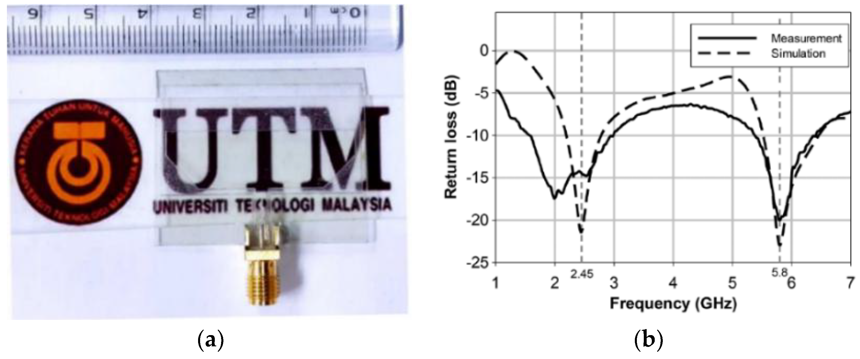
In Reference [35], a CPW dual band meander-line transparent antenna with AgHT-4 film is introduced. A meander-shaped resonant radiator is combined with an inverted U-slot CPW ground plane to take advantage of the compact size and dual band of the antenna. This transparent antenna is printed on a glass substrate with a 2-mm thickness. This AgHT-4 film with dimensions of 30 mm × 30 mm × 0.175 mm has σ = 2.2 × 10⁵ S/m conductivity and Rs = 4 Ω/sq resistance. The proposed antenna has a performance below −10 dB at the dual band frequency referring to the return loss and it yields gains of 2.42 and 2.85 dBi at 2.4 and 5.8 GHz.
2.4.3. Patterned Metal Grid
Using a patterned metal grid is one way to make an optically transparent antenna. This structure features optical transmittance because light is transmitted between the metal grid structures. However, the current still flows because the grids are connected [36]. With metal grids, an advantage is increased optical transmittance compared to continuous metal sheets due to the fact that the area between the grid lines is 100% transparent. However, this increase in transmittance comes at the expense of sheet resistance reduction. If the thickness of the metal grid is greater, the light transmittance is reduced, and therefore a thinner thickness than skin depth is generally required. Thinner than skin depth, however, leads to an increase in sheet resistance, which leads to a decrease in the electrical conductivity and radiation efficiency of the antenna. However, making the line width thinner than the wavelength of light has the additional advantage of minimizing scattering from the film [24].
Au and Ag Grids
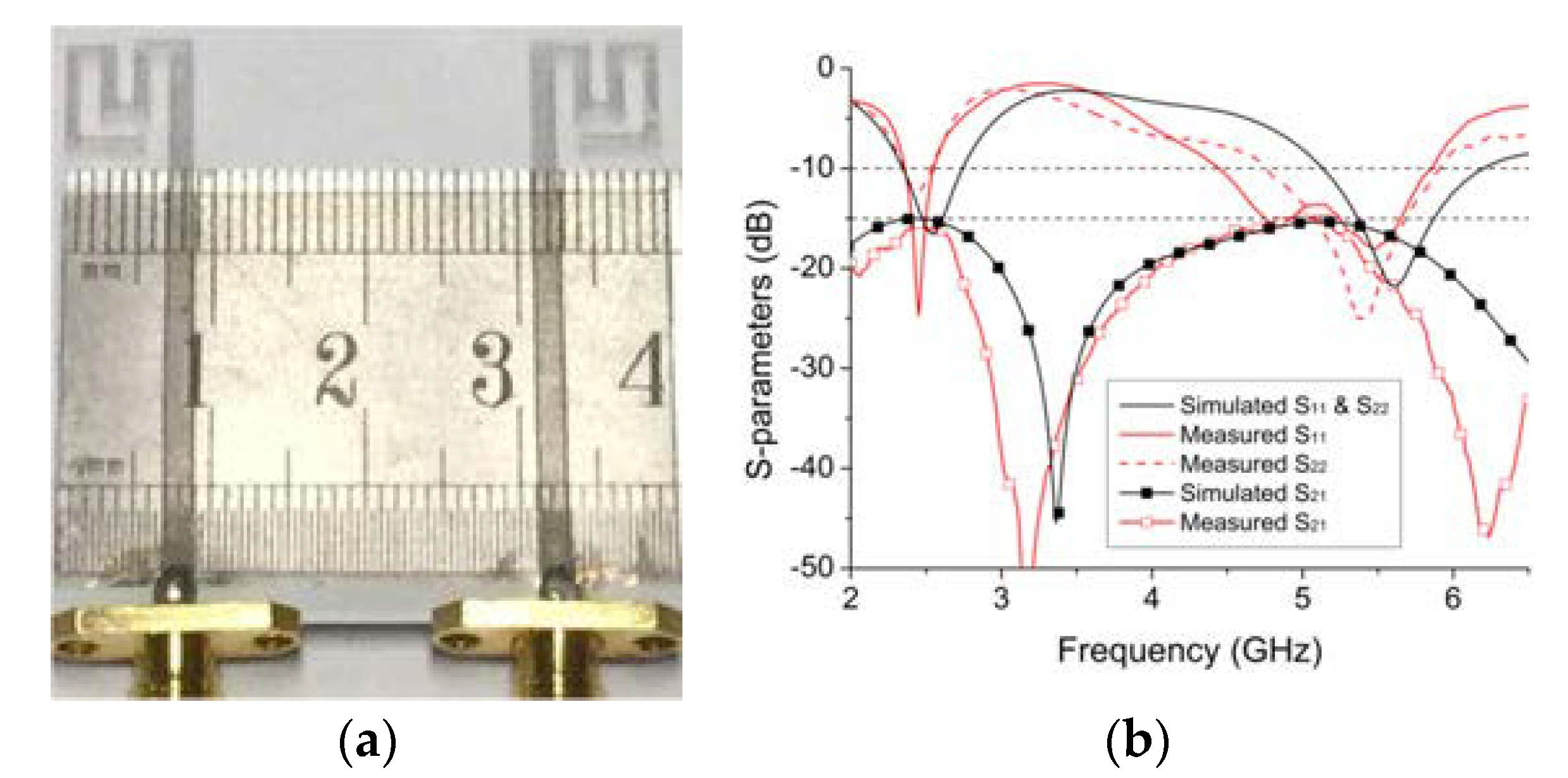
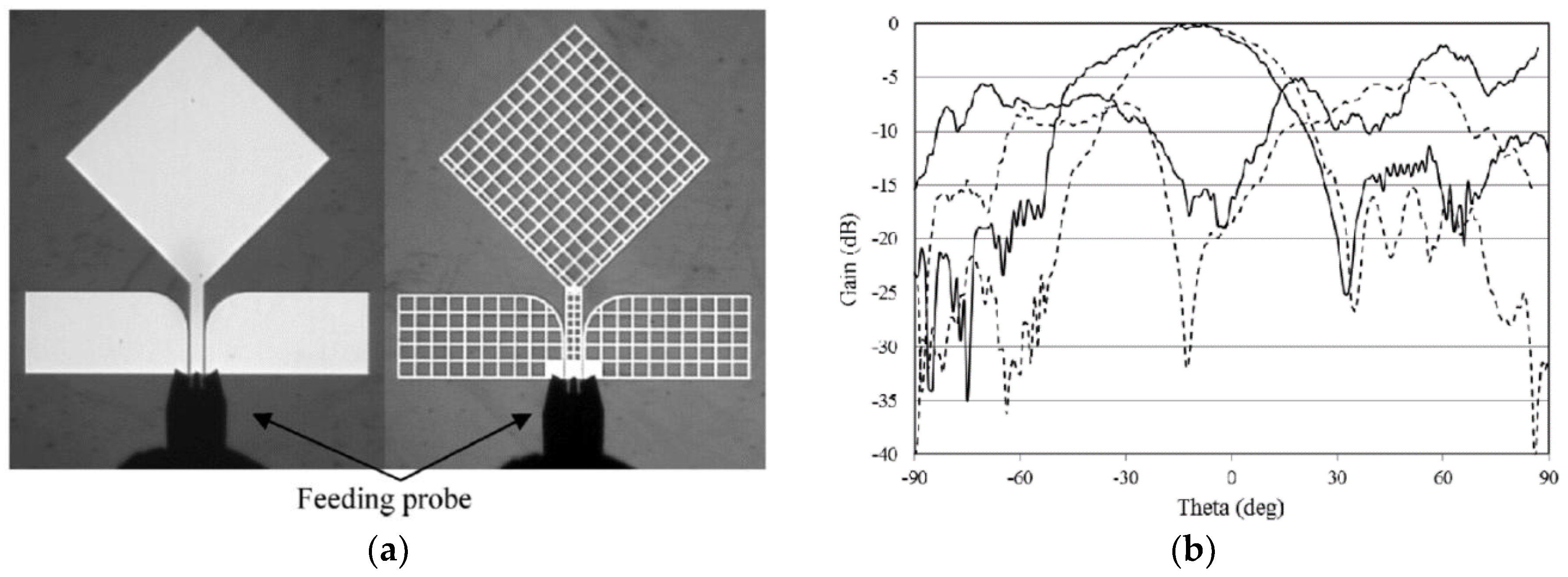
In Reference [36], a gold grid layer (AuGL) CPW-fed planar monopole lozenge antenna operating at 60 GHz is proposed. The structure of AuGL is deposited on a 0.2-mm thick fused silica 7980 Corning substrate with a relative permittivity of 3.8 and a loss tangent of 0.0001. The AuGL has better optical transmittance and sheet resistance than others. The sheet resistance decreases as the metal area increases. The theoretical sheet resistance and the optical transmittance of the AuGL are 0.04 Ω/sq and 83%, respectively (thickness of layer: 1 mm, pitch of the grid: 200 μm, and gold strip grid-width: 10 μm). Figure 10a shows the structure of the fabricated reference antenna and mesh transparent antenna. Notably, there is no difference in radiation efficiency between the reference antenna and the transparent antenna despite the very short wavelength of 54 GHz in Figure 10b.
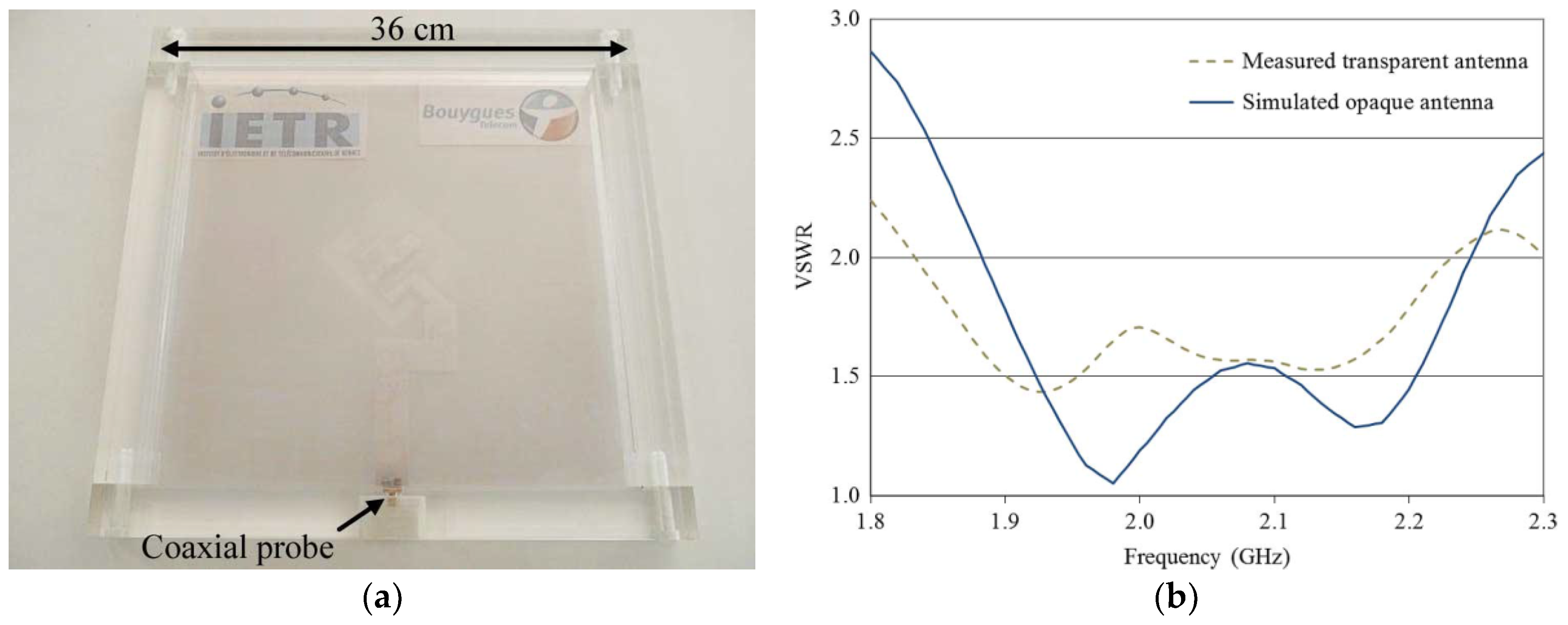
In Reference [37], a multilayer H-shaped slot antenna composed of three silver grid layers (AgGLs) printed on each glass substrate is proposed, as depicted in Figure 11a. It operates in the FDD-UMTS band (1920–2170 MHz), shown in Figure 11b. It is built on three 300 mm × 300 mm × 1.1 mm 1737 Corning glass substrates (with a relative permittivity of 5.7 and a loss tangent of 0.006 at 2 GHz). AgGL features the lowest sheet resistance of 0.054 Ω/sq compared to 8 Ω/sq of ITO and 4.5 Ω/sq of AgHT, so AgGL is used. The theoretical optical transmittance in this antenna structure is between 51.6% and 70.7% over the whole visible light spectrum. It also has a radiation efficiency of 60% (around 5 dBi of antenna gain), compared with 90% of the ideal opaque antenna.
Metal Grid
In Reference [38], a broadside radiating patch antenna consisting of a diamond grid representing the fundamental TM010 mode at 28 GHz is designed. The patch is detailed for a 2000-Å thick Ag alloy with various dielectrics. The patch width and length are 2.5 and 1.8 mm, respectively. This value is obtained by a numerical analysis of multiple substrates consisting of a transparent film insulator, OCA, and display panel. The diamond-grid patch antenna achieves an impedance bandwidth of about 800 MHz, which can cover the Federal Communications Commission (FCC) assigned to the 28 GHz band spectrum for 5G. The measured radiation gain of the diamond-grid patch antenna is confirmed to be 3.2 dBi.
3. Summary of Various Transparent Antennas
The Rs-T performance of TCFs is evaluated using a FoM consisting of σdc/σopt, as expressed in Reference [38]. Table 1 summarizes the results of recently published transparent antennas featuring various TCFs. While graphene [4] and CNT [13] exhibit higher optical transmittances, the electrical sheet resistance remains excessively high for microwave applications. Compared to nano carbons and TCOs, metallic nanostructures feature smaller values of Rs and higher values of T, resulting in enhanced σdc/σopt. In the case of IZTO/Ag/IZTO [20], CuNW [30], and patterned metal grid [36,37], σdc/σopt is remarkable, but the optical transmittance criteria (T > 85%) requires further improvement. However, the optical transmittance of the sample in Reference [38] (T = 88%) meets the aforementioned optical transmittance criteria (the FoM and Rs of the sample in Reference [38] are 887 and 3.22 Ω/sq, respectively). In addition, not only the sheet resistance and optical transmittance, but also the optical degradation such as haze and moiré effects should be considered when placed above substrates, such as active display panels, in future transparent antenna research.
4. Conclusions
In this paper, material-specific transparent antennas from nano carbon to metallic nanostructures are reviewed. Transparent antennas were first devised by National Aeronautics and Space Administration (NASA) for integration with solar cells. Transparent antennas need to be consistently developed autonomously as well as embedded in active display panels to compensate for the low efficiency of electrically small antennas in mobile devices in the 5G world. In other words, a transparent antenna could be a core technology used in the 5G era and should be studied with the concept of Antenna-on-Display (AoD). In addition, to compensate for 5G millimeter-wave degraded channel characteristics, the authors estimate the transparent antenna to be an array consisting of bandwidth >1 GHz, antenna array gain >10 dBi, and far-field radiation efficiency >60%. It is essential to use an antenna array to obtain high gain (high efficiency) so that AoD can easily utilize the entire display area for transparent arrays. Furthermore, the electrical sheet resistance of TCFs must be below a few Ω/sq to secure the gain of a single antenna element and the optical transmittance must be higher than 85.0% to be transparent at the visible spectrum. Optical degradations such as haze and moiré effects when placed above active display panels should be considered when TCFs are selected for transparent antennas. Along with Antenna-in-Package (AiP) and Antenna-on-Chip (AoC) research, AoD needs to be researched as one of critical technologies in 5G communications.
Funding
This research was supported by the Basic Science Research Program through the National Research Foundation of Korea (NRF) funded by the Ministry of Science, ICT, and Future Planning (2017R1C1B501).
Conflicts of Interest
The authors declare no conflict of interest.
References
- Simons, R.N.; Lee, R.Q. Feasibility study of optically transparent microstrip patch antenna. In Proceedings of the IEEE Antennas and Propagation Society International Symposium, Montreal, QC, Canada, 13–18 July 1997. [Google Scholar]
- Zhang, Q.; Wan, X.; Xing, F.; Huang, L.; Long, G.; Yi, N.; Ni, W.; Liu, Z.; Tian, J.; Chen, Y. Solution-processable graphene mesh transparent electrodes for organic solar cells. Nano Res. 2013, 6, 478–484. [Google Scholar] [CrossRef]
- Hu, L.; Wu, H.; Cui, Y. Metal nanogrids, nanowires, and nanofibers for transparent electrodes. MRS Bull. 2011, 36, 760–765. [Google Scholar] [CrossRef]
- Avouris, P. Graphene: Electronic and photonic properties and devices. Nano Lett. 2010, 10, 4285–4294. [Google Scholar] [CrossRef] [PubMed]
- Perruisseau-Carrier, J.; Tamagnone, M.; Gomez-Diaz, J.S.; Carrasco, E. Graphene antennas: Can integration and reconfigurability compensate for the loss? In Proceedings of the 2013 IEEE European Microwave Conference (EuMC), Nuremberg, Germany, 6–10 October 2013; pp. 369–372. [Google Scholar]
- Gomez-Diaz, J.S.; Perruisseau-Carrier, J. Microwave to THz properties of graphene and potential antenna applications. In Proceedings of the 2012 IEEE International Symposium on Antennas and Propagation (ISAP), Nagoya, Japan, 29 October–2 November 2012; pp. 239–242. [Google Scholar]
- Tamagnone, M.; Gomez-Diaz, J.S.; Mosig, J.R.; Perruisseau-Carrier, J. Analysis and design of terahertz antennas based on plasmonic resonant graphene sheets. J. Appl. Phys. 2013, 112, 114915. [Google Scholar] [CrossRef]
- Carrasco, E.; Tamagnone, M.; Perruisseau-Carrier, J. Tunable graphene reflective cells for THz reflectarrays and generalized law of reflection. Appl. Phys. Lett. 2013, 102, 104103. [Google Scholar] [CrossRef]
- Fallahi, A.; Perruisseau-Carrier, J. Design of tunable biperiodic graphene metasurfaces. Phys. Rev. B 2012, 86, 195408. [Google Scholar] [CrossRef]
- Iijima, S. Helical microtubules of graphitic carbon. Nature 1991, 354, 56. [Google Scholar] [CrossRef]
- Vacirca, N.A.; McDonough, J.K.; Jost, K.; Gogotsi, Y.; Kurzweg, T.P. Onion-like carbon and carbon nanotube film antennas. Appl. Phys. Lett. 2013, 103, 073301. [Google Scholar] [CrossRef]
- Elwi, T.A.; Al-Rizzo, H.M.; Rucker, D.G.; Dervishi, E.; Li, Z.; Biris, A.S. Multi-walled carbon nanotube-based RF antennas. Nanotechnology 2009, 21, 045301. [Google Scholar] [CrossRef] [PubMed]
- Tung, V.C.; Chen, L.M.; Allen, M.J.; Wassei, J.K.; Nelson, K.; Kaner, R.B.; Yang, Y. Low-temperature solution processing of grapheme–carbon nanotube hybrid materials for high-performance transparent conductors. Nano Lett. 2009, 9, 1949–1955. [Google Scholar] [CrossRef] [PubMed]
- Shimoni, A.; Azoubel, S.; Magdassi, S. Inkjet printing of flexible high-performance carbon nanotube transparent conductive films by “coffee ring effect”. Nanoscale 2014, 6, 11084–11089. [Google Scholar] [CrossRef] [PubMed]
- Kim, Y.-K.; Min, D.-H. Durable large-area thin films of graphene/carbon nanotube double layers as a transparent electrode. Langmuir 2009, 25, 11302–11306. [Google Scholar] [CrossRef] [PubMed]
- Ali, N.M.; Misran, N.; Mansor, M.F.; Jamlos, M.F. Transparent solar antenna of 28 GHz using transparent conductive oxides (TCO) thin film. J. Phys. Conf. Ser. 2017, 852, 012036. [Google Scholar]
- Thampy, A.S.; Dhamodharan, S.K. Performance analysis and comparison of ITO-and FTO-based optically transparent terahertz U-shaped patch antennas. Phys. E 2015, 66, 52–58. [Google Scholar] [CrossRef]
- Colombel, F.; Castel, X.; Himdi, M.; Legeay, G.; Vigneron, S.; Cruz, E.M. Ultrathin metal layer, ITO film and ITO/Cu/ITO multilayer towards transparent antenna. IET Sci. Meas. Technol. 2009, 3, 229–234. [Google Scholar] [CrossRef]
- Choi, K.H.; Nam, H.J.; Jeong, J.A.; Cho, S.W.; Kim, H.K.; Kang, J.W.; Kim, D.G.; Cho, W.J. Highly flexible and transparent InZnSnOx/Ag/InZnSnOx multilayer electrode for flexible organic light emitting diodes. Appl. Phys. Lett. 2008, 92, 3302–3305. [Google Scholar] [CrossRef]
- Hong, S.; Kim, Y.; Jung, C.W. Transparent microstrip patch antennas with multilayer and metal-mesh films. IEEE Antennas Wirel. Propag. Lett. 2017, 16, 772–775. [Google Scholar] [CrossRef]
- Chiang, C.K.; Fincher, C.R., Jr.; Park, Y.W.; Heeger, A.J.; Shirakawa, H.; Louis, E.J.; Gau, S.C.; MacDiarmid, A.G. Electrical conductivity in doped polyacetylene. Phys. Rev. Lett. 1977, 39, 1098. [Google Scholar] [CrossRef]
- Kirsch, N.J.; Vacirca, N.A.; Plowman, E.E.; Kurzweg, T.P.; Fontecchio, A.K.; Dandekar, K.R. Optically transparent conductive polymer RFID meandering dipole antenna. In Proceedings of the 2013 IEEE International Conference on RFID, Orlando, FL, USA, 30 April–2 May 2013; pp. 278–282. [Google Scholar]
- Rmili, H.; Miane, J.L.; Zangar, H.; Olinga, T. Design of microstrip-fed proximity-coupled conducting-polymer patch antenna. Microw. Opt. Technol. Lett. 2006, 48, 655–660. [Google Scholar] [CrossRef]
- Lee, J.; Lee, P.; Lee, H.B.; Hong, S.; Lee, I.; Yeo, J.; Lee, S.S.; Kim, T.S.; Lee, D.; Ko, S.H. Room-temperature nanosoldering of a very long metal nanowire network by conducting-polymer-assisted joining for a flexible touch-panel application. Adv. Funct. Mater. 2013, 23, 4171–4176. [Google Scholar] [CrossRef]
- Hecht, D.S.; Hu, L.; Irvin, G. Emerging transparent electrodes based on thin films of carbon nanotubes, graphene, and metallic nanostructures. Adv. Mater. 2011, 23, 1482–1513. [Google Scholar] [CrossRef] [PubMed]
- Hu, L.; Kim, H.S.; Lee, J.Y.; Peumans, P.; Cui, Y. Scalable coating and properties of transparent, flexible, silver nanowire electrodes. ACS Nano 2010, 4, 2955–2963. [Google Scholar] [CrossRef] [PubMed]
- Dao, Q.H.; Tchuigoua, R.; Geck, B.; Manteuffel, D.; von Witzendorff, P.; Overmeyer, L. Optically transparent patch antennas based on silver nanowires for mm-wave applications. In Proceedings of the 2017 IEEE International Symposium on Antennas and Propagation & USNC/URSI National Radio Science Meeting, San Diego, CA, USA, 9–14 July 2017; pp. 2189–2190. [Google Scholar]
- Rai, T.; Dantes, P.; Bahreyni, B.; Kim, W.S. A stretchable RF antenna with silver nanowires. IEEE Electron Device Lett. 2013, 34, 544–546. [Google Scholar] [CrossRef]
- Song, L.; Myers, A.C.; Adams, J.J.; Zhu, Y. Stretchable and reversibly deformable radio frequency antennas based on silver nanowires. ACS Appl. Mater. Interfaces 2014, 6, 4248–4253. [Google Scholar] [CrossRef] [PubMed]
- Li, Q.L.; Cheung, S.W.; Wu, D.; Yuk, T.I. Optically transparent dual-band MIMO antenna using micro-metal mesh conductive film for WLAN system. IEEE Antennas Wirel. Propag. Lett. 2017, 16, 920–923. [Google Scholar] [CrossRef]
- Sa’ad, B.M.; Rahim, S.K.A.; Peter, T.; Rani, M.S.B.A.; Ausordin, S.F.; Zaidel, D.N.A.; Krishnan, C. Transparent branch-line coupler using micro-metal mesh conductive film. IEEE Microw. Wirel. Compon. Lett. 2014, 2, 857–859. [Google Scholar] [CrossRef]
- Yun, J. Ultrathin metal films for transparent electrodes of flexible optoelectronic devices. Adv. Funct. Mater. 2017, 27, 1606641. [Google Scholar] [CrossRef]
- Optical Filters for Electronic Displays. Available online: http://www.instrumentplastics.co.uk/products/ito-film-and-ito-coatings (accessed on 30 April 2018).
- Malek, M.A.; Hakimi, S.; Rahim, S.A.; Evizal, A.K. Dual-band CPW-fed transparent antenna for active RFID tags. IEEE Antennas Wirel. Propag. Lett. 2015, 14, 919–922. [Google Scholar] [CrossRef]
- Jizat, N.M.; Rahim, S.K.A.; Lo, Y.C.; Mansor, M.M. Compact size of CPW dual-band meander-line transparent antenna for WLAN applications. In Proceedings of the 2014 IEEE Asia-Pacific Conference on Applied Electromagnetics (APACE), Johor Bahru, Malaysia, 8–10 December 2014; pp. 20–22. [Google Scholar]
- Hautcoeur, J.; Talbi, L.; Hettak, K. Feasibility study of optically transparent CPW-fed monopole antenna at 60-GHz ISM bands. IEEE Trans. Antennas Propag. 2013, 61, 1651–1657. [Google Scholar] [CrossRef]
- Hautcoeur, J.; Colombel, F.; Himdi, M.; Castel, X.; Cruz, E.M. Large and optically transparent multilayer for broadband H-shaped slot antenna. IEEE Antennas Wirel. Propag. Lett. 2013, 12, 933–936. [Google Scholar] [CrossRef]
- Lee, S.Y.; Choi, D.; Youn, Y.; Hong, W. Electrical characterization of highly efficient, optically transparent nanometers-thick unit cells for antenna-on-display applications. In Proceedings of the 2018 IEEE MTT-S International Microwave Symposium (IMS), Philadelphia, PA, USA, 10–15 June 2018. [Google Scholar]
Figure 1.
Real (a) and imaginary (b) parts of graphene conductivity versus chemical potential. Graphene parameters are τ = 0.5 ps and T = 300 °K [5]. (With permission from IEEE).
Figure 1.
Real (a) and imaginary (b) parts of graphene conductivity versus chemical potential. Graphene parameters are τ = 0.5 ps and T = 300 °K [5]. (With permission from IEEE).

Figure 2.
Analysis of (a) radiation efficiency of an ideal lossless antenna and real graphene-based patch antennas at microwaves [5] and (b) Input impedance Zin of the proposed antennas. The arrows indicate the real impedance W.P. [7]. (With permission from IEEE and AIP).

Figure 3.
(a) Onion-like carbon (OLC) antenna; (b) return loss versus frequency of OLC, carbon nanotubes (CNT), and copper antennas [11]. (With permission from AIP).
Figure 3.
(a) Onion-like carbon (OLC) antenna; (b) return loss versus frequency of OLC, carbon nanotubes (CNT), and copper antennas [11]. (With permission from AIP).

Figure 4.
(a) Structure of designed antenna [16] and (b) frequency versus return loss (dB) for the antennas [17]. (With permission from Elsevier and IOP).
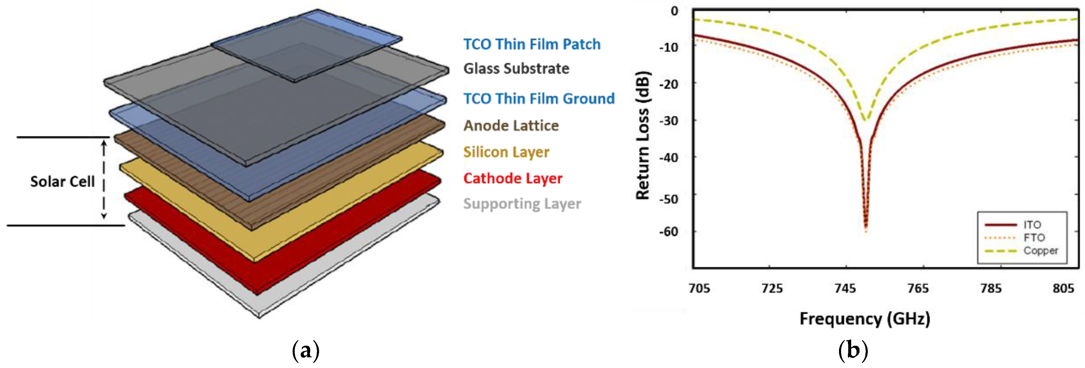
Figure 5.
(a) Fabricated microstrip patch antenna and (b) simulated and measured reflection coefficients of the proposed antenna [20]. (With permission from IEEE).
Figure 5.
(a) Fabricated microstrip patch antenna and (b) simulated and measured reflection coefficients of the proposed antenna [20]. (With permission from IEEE).

Figure 6.
(a) Pictures of a radio frequency identification (RFID) half wavelength dipole antenna and (b) an RFID meandering dipole antenna and diagram [22]. (With permission from IEEE).
Figure 6.
(a) Pictures of a radio frequency identification (RFID) half wavelength dipole antenna and (b) an RFID meandering dipole antenna and diagram [22]. (With permission from IEEE).

Figure 7.
(a) Model of the investigated patch antenna and microscopic image of a single silver nanowire (AgNW) coating with 67.9% optical transmission at 550 nm; (b) simulation radiation pattern of the patch antenna operating at 61 GHz [27]. (With permission from IEEE).
Figure 7.
(a) Model of the investigated patch antenna and microscopic image of a single silver nanowire (AgNW) coating with 67.9% optical transmission at 550 nm; (b) simulation radiation pattern of the patch antenna operating at 61 GHz [27]. (With permission from IEEE).

Figure 8.
(a) Prototyped transparent micro metal mesh conductive film antenna; (b) simulated and measured S-parameters of the proposed antenna [30]. (With permission from IEEE).
Figure 8.
(a) Prototyped transparent micro metal mesh conductive film antenna; (b) simulated and measured S-parameters of the proposed antenna [30]. (With permission from IEEE).

Figure 9.
(a) Photograph of the fabricated antenna using the AgHT-8 transparent thin film; (b) simulated and measured return loss of the proposed antenna [34]. (With permission from IEEE).
Figure 9.
(a) Photograph of the fabricated antenna using the AgHT-8 transparent thin film; (b) simulated and measured return loss of the proposed antenna [34]. (With permission from IEEE).

Figure 10.
Photographs of the coplanar-fed monopole lozenge antennas printed on fused silica 7980 Corning substrates under measurement. (a) Light reflecting reference antenna and meshed transparent antenna; (b) Measured radiation patterns (co-polarization and cross-polarization) of the two monopole antennas at 54 GHz. Solid line: reference antenna; dotted line: optically transparent antenna [36]. (With permission from IEEE).

Figure 11.
(a) Broadband optically transparent H-shaped slot antenna above the lab logo; (b) computed and measured VSWR of the broadband H-shaped slot antenna from 1.8 to 2.3 GHz [37]. (With permission from IEEE).
Figure 11.
(a) Broadband optically transparent H-shaped slot antenna above the lab logo; (b) computed and measured VSWR of the broadband H-shaped slot antenna from 1.8 to 2.3 GHz [37]. (With permission from IEEE).


Table 1.
RS-T performance parameters of transparent conductive films (TCFs).
| Materials | Ref. | Details | Rs (Ω/sq) | T (%) | FoM |
|---|---|---|---|---|---|
| Nano Carbons | [5] | Graphene | N.A. | N.A. | - |
| [6] | Graphene | N.A. | N.A. | - | |
| [4] | Graphene | 30 | 90 | 116.2 | |
| [11] | OLC and MWCNT | N.A. | N.A. | - | |
| [12] | MWCNT | N.A. | N.A. | - | |
| [13] | CNT | 280 | 90 | 12.4 | |
| Transparent Conductive Oxides (TCOs) | [16] | ITO | 10 | N.A. | - |
| [17] | FTO | 24 | N.A. | - | |
| [18] | ITO/CU/ITO | 4.7 | 61 | 143.0 | |
| [20] | IZTO/Ag/IZTO | 2.52 | 80 | 663.7 | |
| Conductive Polymers | [22] | PEDOT-PSS | N.A. | N.A. | - |
| [23] | - | N.A. | N.A. | - | |
| [24] | AgNW/PEDOT:PSS | 25 | 90 | 139.4 | |
| Metallic Nanostructures | [27] | AgNW | 0.36 | 51 | 1308.1 |
| [28] | AgNW | 5 | N.A. | - | |
| [30] | CuNW | 0.05 | 75 | 24,369.6 | |
| [31] | CuNW | 0.7 | 75 | 1740.7 | |
| [34] | AgHT-8 | 8 | 80 | 199.6 | |
| [34] | AgHT-4 | 4 | N.A. | - | |
| [36] | AuGL | 0.44 | 83 | 4387.5 | |
| [37] | AgGL | 0.054 | 81.3 | 32,007.8 | |
| [38] | Metal grid | 3.22 | 88 | 887.0 |
© 2018 by the authors. Licensee MDPI, Basel, Switzerland. This article is an open access article distributed under the terms and conditions of the Creative Commons Attribution (CC BY) license (http://creativecommons.org/licenses/by/4.0/).
Share and Cite
MDPI and ACS Style
Lee, S.Y.; Choo, M.; Jung, S.; Hong, W. Optically Transparent Nano-Patterned Antennas: A Review and Future Directions. Appl. Sci. 2018, 8, 901. https://doi.org/10.3390/app8060901
AMA Style
Lee SY, Choo M, Jung S, Hong W. Optically Transparent Nano-Patterned Antennas: A Review and Future Directions. Applied Sciences. 2018; 8(6):901. https://doi.org/10.3390/app8060901
Chicago/Turabian StyleLee, Seung Yoon, Moogoong Choo, Sohyeon Jung, and Wonbin Hong. 2018. "Optically Transparent Nano-Patterned Antennas: A Review and Future Directions" Applied Sciences 8, no. 6: 901. https://doi.org/10.3390/app8060901
Note that from the first issue of 2016, this journal uses article numbers instead of page numbers. See further details here.