Article

Numerical Simulation of Temperature Fields in a Three-Dimensional SiC Crystal Growth Furnace with Axisymmetric and Spiral Coils

1
Energy Research Institute, Qilu University of Technology (Shandong Academy of Sciences), Jinan 250014, China
2
Shandong Shenhua Shanda Energy & Environment Co., Ltd., Jinan 250014, Shandong, China
3
Shandong Shenzhou Electric Furnace Co., Ltd., Linyi 276000, Shandong, China
*
Authors to whom correspondence should be addressed.
Appl. Sci. 2018, 8(5), 705; https://doi.org/10.3390/app8050705
Submission received: 9 April 2018 / Revised: 20 April 2018 / Accepted: 20 April 2018 / Published: 2 May 2018
(This article belongs to the Section Materials Science and Engineering)

Abstract

:
Three-dimensional numerical simulation platform for silicon carbide crystal growth furnace was established using C programing language, where a physical model of the furnace was built based on cylindrical coordinates; governing equations for electromagnetic and temperature fields were discretized by finite volume method; radiation characteristics were studied with the help of S2S model (surface to surface radiation model); and the least distance method was proposed to check radiation faces visibility efficiently. LU decomposition algorithm based on graphic processing unit (GPU) technology was developed to accelerate the solving process of surface to surface radiation. Then the radiation heat transfer in silicon carbide crystal (SiC) growth chamber and temperature field of silicon carbide growth furnace were studied quantificationally at I = 1250 A and F = 16 kHz. The effects of coil structures (axisymmetric and spiral) on temperature field and its gradient distributions were investigated by standard deviation method. The simulation results demonstrate that spiral electromagnetic coil generates non-axisymmetric temperature field easily; the radiation heat flux is 102~103 times more than conduction heat flux, radiation heat transfer is helpful to increase temperature evenness; the spiral temperature field on the SiC crystal cross-section reduces the poor homogeneity of temperature gradient, which will cause crystal to generate large defects.

Graphical Abstract

1. Introduction

Silicon carbide crystal (SiC) crystals are used to product semiconductor devices under higher-temperature, higher-frequency, and higher-power conditions [1]. Compared with silicon, silicon carbide crystal has better performance on chemical and thermal properties, such as higher thermal conductivity, chemical stability, radiation stability, and mechanical stability [2]. The physical vapor transport (PVT) method is the most successful and common method to grow SiC crystals at pressure ≤ 50 mbar, increasing crystal growth rate [3,4,5]. In this method, graphite crucible is heated by induction coils and the temperature in the furnace reaches more than 2300 K. The temperature distribution is fatal to SiC growth process, which decides the SiC growth speed and the product quality. However, it is difficult to measure temperature in a confined silicon carbide crystal growth furnace at both high temperature and low pressure, and so far, the infrared thermometry method is adopted to monitor temperature through a gap cooler hole. The detailed study of temperature distribution in the furnace is beneficial to the modification of the furnace structure and operation system.
With the development of computer technology, numerical simulation is becoming a powerful tool to analyze temperature fields [3,6,7,8,9], crystal growth processes [10,11,12], and thermal stresses [13] as the SiC grows. These parameters are meaningful to optimize the process of crystal growth. Both conduction and radiation are the main two heat transfer processes in 2~4 inches SiC crystal growth furnaces. The weaker convection heat transfer is always ignored. For radiation heat transfer, species in the growth chamber are not participated in radiation process, so the surface to surface (S2S) radiation model is used to calculate radiation heat flux [2,14,15,16]. The axisymmetric assumption is adopted in the majority of numerical simulation research, so the model is two-dimensional, the effect of non-axisymmetric coils on electromagnetic field and temperature field are always missed artificially. Moreover, some graphite crucible surfaces cannot see other surfaces because of the nontransparent crystal. Therefore, some methods should be developed to check whether radiation surfaces are visible to other surfaces or not, ensuring the accurate calculation of radiation heat flux.
Herein, a three-dimensional numerical simulation algorithm was developed based on cylindrical coordinate system and C programing language to study the effects of axisymmetric model and spiral coils on electromagnetic and temperature fields at coil current I = 1250 A and current frequency F = 16 kHz. The least distance method is proposed to check visibility of radiation facing to others, and a parallel LU decomposition algorithm for radiation view factor matrix based on graphic processing unit technology is developed to accelerate the solution of surface to surface radiation heat transfer.

2. Modeling of Induction Heating and Heat Transfer

Radio frequency (RF) induction heating technology is used to heat the silicon carbide crystal growth furnace. The reasonable temperature field is premised on an accurate electromagnetic field. Generally, mathematical models for the electromagnetic field are developed based on the Maxwell Equation (1)
{ · E = ρ μ 0 · B = 0 × E = B t × B = μ 0 ε 0 E t + μ 0 ( J c + J i )
where E and B are electric field intensity and magnetic induction intensity, respectively; μ0 (4π × 10−7 H/m) is permeability of free space; ε0 (8.855 × 10⁻¹² F/m in vacuum) is permittivity of free space; Jc is current flux in coil; and Ji (A/m2) is induction current flux in graphite crucible.
To simplify Maxwell equations, magnetic potential, A (B = ∇ × A), is introduced and the simplified equation is proposed in 3D cylindrical coordinates
1 r r ( r A r ) + 1 r 2 2 A θ 2 + 2 A z 2 ( A r 2 + i μ 0 σ ω A + μ 0 J c ) = 0
A can be expressed by (0, A0, 0), and A0 = A0r + iA0i, so Equation (2) can be rewrote as [7,17]
{ 1 r r ( r A 0 r r ) + 1 r 2 2 A 0 r θ 2 + 2 A 0 r z 2 A 0 r r 2 + μ 0 σ ω A 0 i + μ 0 J c = 0 1 r r ( r A 0 i r ) + 1 r 2 2 A 0 i θ 2 + 2 A 0 i z 2 A 0 i r 2 μ 0 σ ω A 0 r = 0
where ω is angular velocity (rad/s, ω = 2πF) and F is current frequency (Hz); Jc is current flux in coil (A/m2, Jc = I/Acoil) and I is current (A), Acoil is area of coil cross section; σ (1.1 × 10⁵ Ω−1·m−1) is coil electric conductivity.
For the different subsystems—such as crystals, silicon carbide powder, graphite crucible, insulation layer, and air of outside furnace—the heat transfer process can be described as the following energy Equation (4)
λ [ 1 r r ( r T r ) + 1 r 2 2 T θ 2 + 2 T z 2 ] + Q e d d y + Q I F = 0
where Qeddy is induction heating source term in the graphite crucible; QIF is heating source term acting on cell interfaces, such as radiation and convection heat exchange (Qinsu) on felt walls, radiation heat exchange (Qrad) on growth chamber walls.
Equations (1) and (2) are discretized by the finite volume method, and solved by the SIMPLE algorithm.
Qeddy as the induction heating source is calculated by [2,18]
Q e d d y = 1 2 σ ω 2 ( A 0 r 2 + A 0 i 2 )
The third boundary condition is used to describe heat release on the felt walls, and the heating source can be added into Equation (2) with the additional source terms method
{ λ T n | w a l l = h ( T T f ) + σ ε ( T 4 T f 4 ) = [ h + σ ε ( T + T f ) ( T 2 + T f 2 ) ] h e f f ( T T f ) S C , a d , i n s u = A Δ V T f 1 / h e f f + δ / λ , S P , a d , i n s u = A Δ V 1 1 / h e f f + δ / λ
where n is vector normal to outer wall. h is convection heat transfer coefficient between the insulation layer and air, σ is the Boltzmann constant (5.67 × 10⁻⁸ W/(m2·K4), e is surface radiation coefficient, heff is the equivalent heat transfer coefficient of convection and radiation heat transfer, d is the grid length in the radial direction, M is the circumference grid area of the volume mesh on the insulation layer, ΔV is the grid volume, and Tf is the fluid temperature. SC,ad,insu and SP,ad,insu are source terms for solving algebraic equations of wall temperatures.

3. Three-Dimensional Silicon Carbide Crystal Growth Furnace

Figure 1 shows a three-dimensional geometry and meshes for silicon carbide crystal growth furnace. To decrease calculation capacity, the electromagnetic and temperature fields are decoupled. Their physical models are presented in Figure 1a,b, respectively. Figure 1c indicates the mesh for physical model in Figure 1a. As shown in the figure, more fine meshes are used for silicon carbide crystal, silicon carbide powder and graphite crucible to get more accurate simulation results. It can be seen from Figure 1a that the coil is quasi-sprial, and the size of its cross section is 10 × 10 mm. The silicon carbide crystal is 50 mm in diameter and 5 mm in height. Graphite crucible is 125 mm in inner diameter, 6 mm thick in r-direction, and 20 mm thick in z-direction. Silicon carbide powder and growth chamber are 55 mm and 25 mm in height, respectively. The furnace is cooled by both top hole with diameter of 20 mm and bottom hole with diameter of 10 mm in diameter. The convection heat transfer coefficient of cooling water (T = 300 K) is 1000 W/(m2·K). The felt is 37 mm thick in r-direction and 40 mm thick in z-direction. The convection heat transfer coefficient of air outside of the furnace (T = 300 K) is 50 W/(m2·K).
Table 1 lists properties of several materials, such as density, heat capacity, heat conductivity coefficient. Properties of porous silicon carbide powder are calculated by φSiC_powder = εφSiC + (1 − εfluid, where ε is void fraction and equals to 0.45.

4. Radiation Heat Transfer in Crystal Growth Chamber

4.1. Surface Visibility Checking Algorithm for S2S Radiation Model

The classical surface to surface (S2S) radiation model is
{ q r = ( A 1 · B ) · ( σ T 4 ) A j k = δ j k ε k F j k 1 ε k ε k , B j k = δ j k F j k F j k = 1 A j A j A k cos θ j cos θ k π d 2 η j k d A j d A k
where A and B are coefficient matrixes of view factors (F); when j = k, δjk = 1, otherwise δjk = 0; T is wall temperature; ηjk = 1 in Fij means face j can see face k, otherwise ηjk = 0. So ηjk should be determined before calculating Fij.
The radiation source term, Qrad, is added into energy equation by qr as the following forms [13]
{ s o l i d : S C , a d , r a d = A Δ V s q r δ f f / λ f δ s f / λ s + δ f f / λ f f l u i d : S C , a d , r a d = A Δ V f q r δ s f / λ s δ s f / λ s + δ f f / λ f T s f = T s λ s / δ s f + T f λ f / δ f f q r λ s / δ s f λ f / δ f f λ s / δ s f + λ f / δ f f
where δsf and δff are distances from the center of solid mesh cell and fluid mesh cell to the fluid–solid interface center.
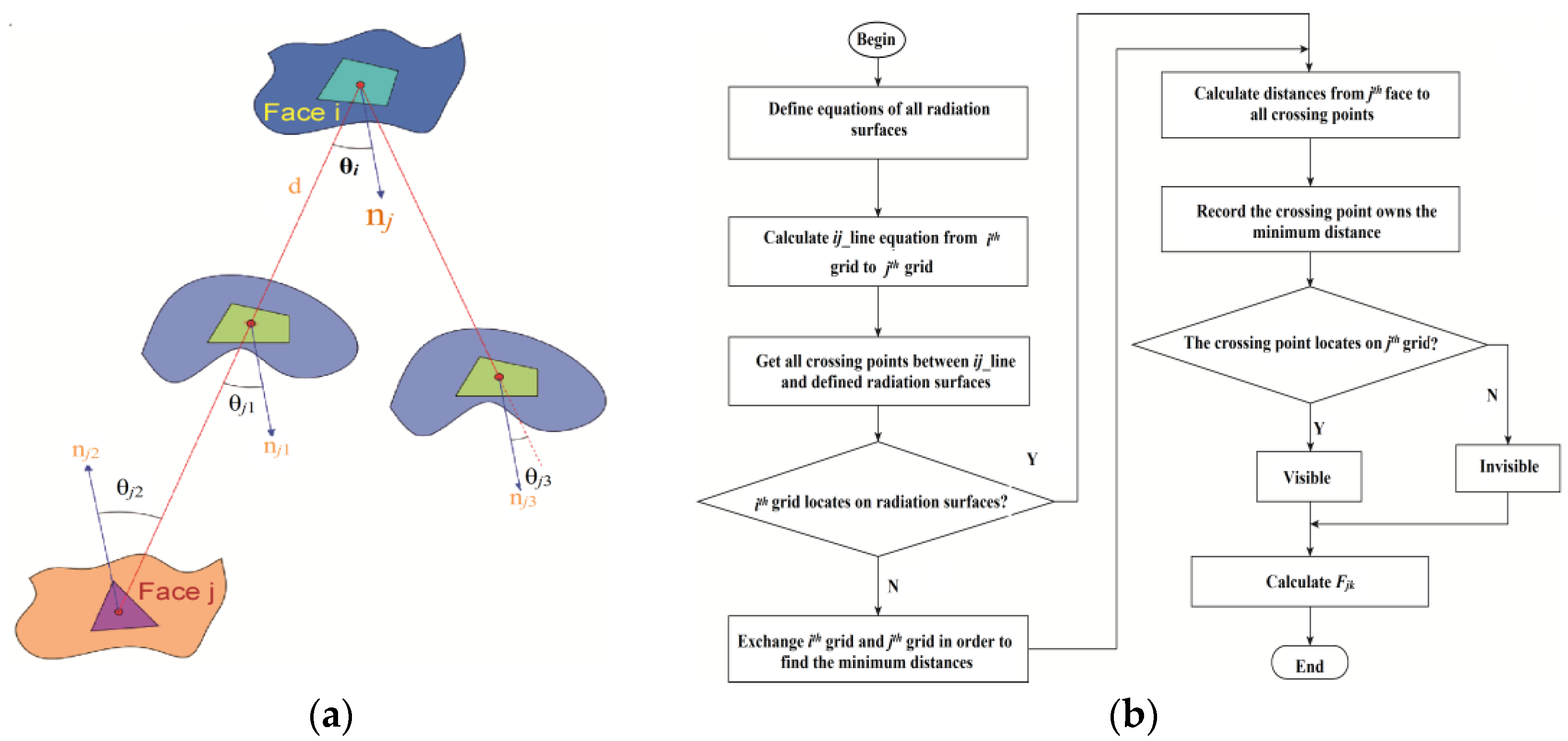
Least distance method (LDM) is proposed to determine the value of ηjk between two wall faces. Figure 2 exhibits a schematic diagram and a flowchart of LDM. An example (ith cell face) is given to illustrate the principle of LDM: (1) give the mathematical forms (F(R)) of block faces, such as growth surface and cylindrical surface of silicon carbide crystal; (2) search all other jth cell faces and save their face information as shown in Figure 2a, such as normal vector n, distance vector d, position coordinates of face center, line equation L(i, j) from ith face center to jth face center, angle θi and θj between n and d; (3) calculate and save all intersection points (P(L, F)) between line L(i, j) and face F(R); (4) calculate all distances from ith face center to P(L, F) and record the point owning a minimum distance; (5) check whether the recorded point coincides with jth face center or not, if not then ηij = 1, otherwise ηij = 0.
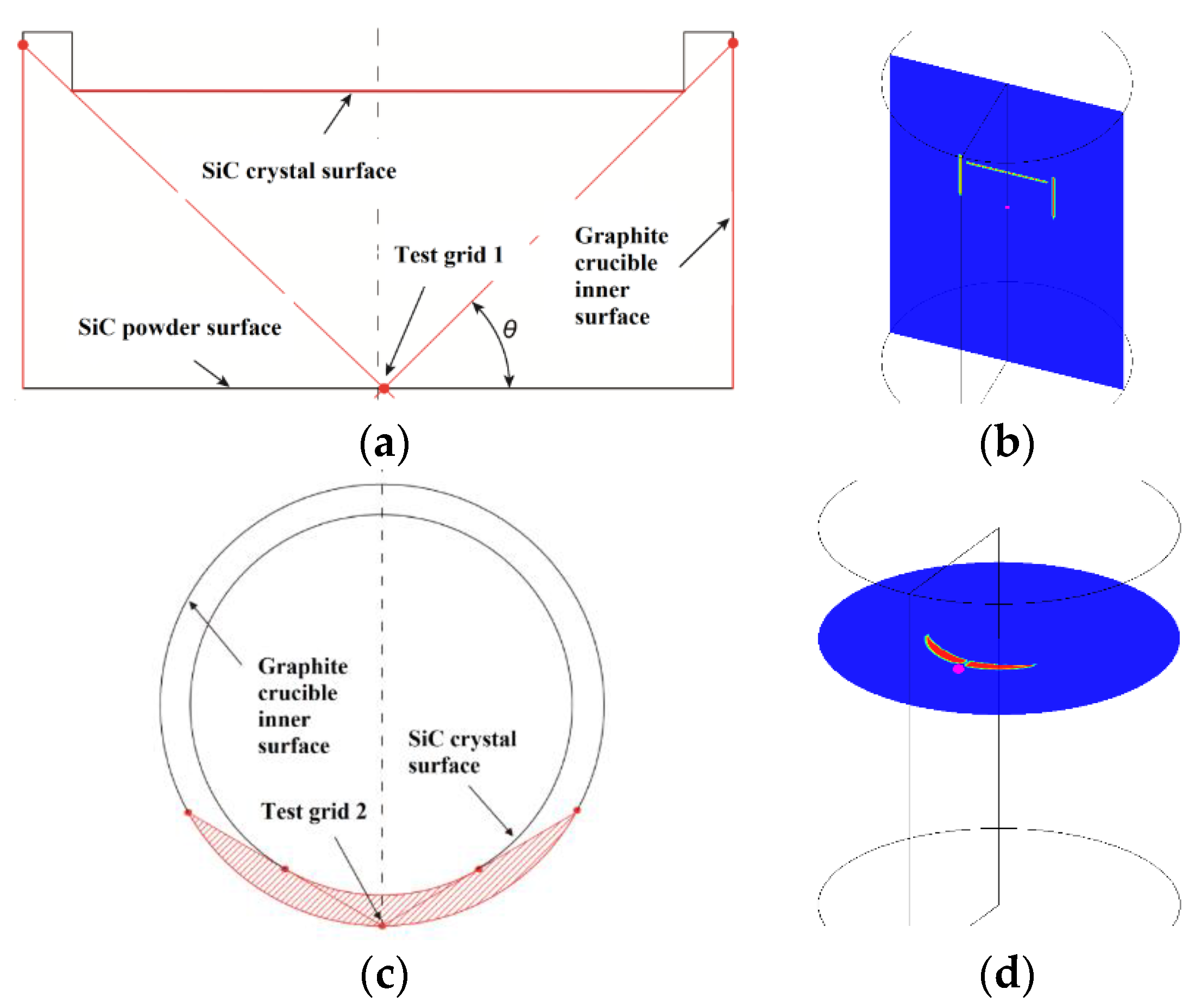
Two wall faces (located on SiC powder surface 1# mesh face and graphite crucible inner surface (2# mesh face)) are selected to verify LDM as shown in Figure 3. The red regions as shown in Figure 3a,c are ideal visible region for 1# mesh face and 2# mesh face, respectively. By comparing of Figure 3a,b, it can be seen that calculated visible region is as same as ideal visible region which locates on graphite cylindrical wall and crystal growth wall. Similar results are shown in Figure 3c,d. These simulation results can be demonstrated that LDM is an efficient and accurate method to check whether radiation faces can see other faces or not.

4.2. Acceleration to Solve S2S Radiation Heat

Matrix A and B in Equation (7) are only relevant with radiation view factors which are determined by physical geometry and meshes. With the increase of mesh number in growth chamber, the calculation capacity increases sharply, not only do matrix A and B need more memory, but also it will take more time for a CPU (central processing unit) to calculate qr. For purpose of solving this problem, constant matrix C is introduced to simplify Equation (7), and matrix C is solved by matrix A and B
{ q r = C · ( σ T 4 ) A C = B
Here, the matrix C was solved by LU decomposition algorithm (which was an algorithm to solve linear algebraic equations) based on parallel GPU codes, and the models of Equations (3)–(8) were solved by a serials of CPU codes. All the simulation works were finished on a workstation with 8 CPUs and 32G memory. The GPU codes were run on a GeForce GTX 580: NVIDIA, Santa Clara, CA, USA graphics card, which owns 512 stream processors and 1536 MB video memory.
For the same mesh and the same physical model, the pre-solved and pre-saved matrix C can be read into the program which will save much time to solve Equation (7). To further improve calculation efficiency, a parallel LU decomposition algorithm based on GPU technology is used. Four cases are set up in order to compare calculation efficiency by CPU and GPU with different mesh numbers, and the time consuming results are listed as shown in Table 2. It can be found that GPU costs less time to get the matrix C than CPU. GPU technology also indicated the faster calculation efficiency with the increase of mesh size. In addition, the temperature difference (ΔT) between crystal surface and SiC powder surface is compared with different mesh size. It can be seen that ΔT for the four cases are close to each other, so 56 × 43 × 71 is chosen to get accurate temperature field and decrease calculation capacity.

5. Test of Mesh Independence

In addition, four mesh sizes listed in Table 3 are compared with each other in order to investigate the relationship between mesh size and both calculation accuracy and calculation efficiency. 2304, 4320, 5184, and 6912 radiation faces are generated in the growth chamber for the four cases, respectively.
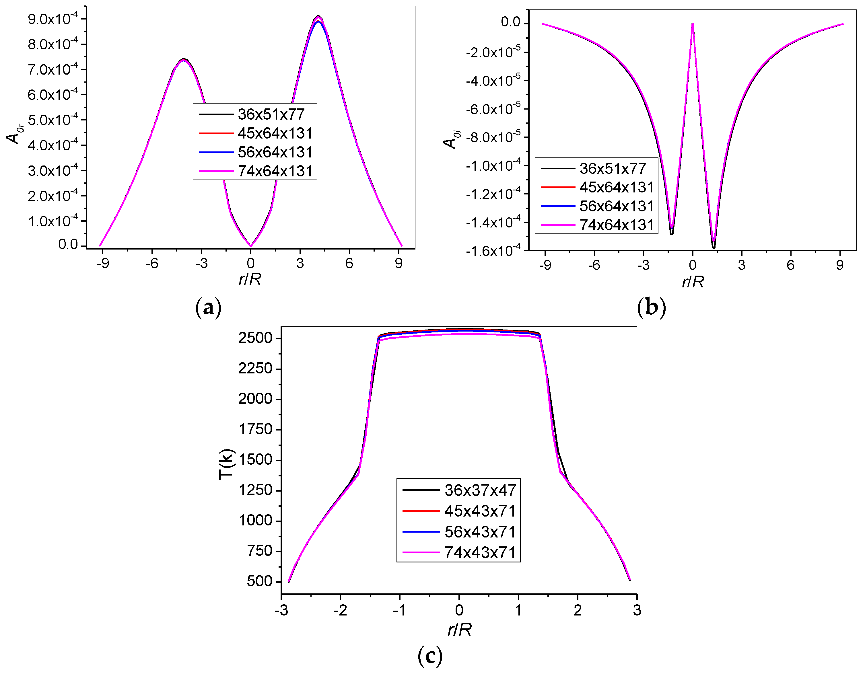
Figure 4 shows profiles of magnetic potential and temperature along with radius. For A0r and A0i presented in Figure 4a,b, the results of case 2, 3 and 4 are in good agreement with each other, which illustrates that meshes for electromagnetic field are fine enough. As seen in Figure 4c, the similar temperature profiles are presented for case 1, 2 and 3, temperature profile of case 4 is slightly lower than those of case 1, 2 and 3. This is because more radiation surfaces reduce to bigger calculation error. Based on the above analysis, 56 × 64 × 131 for electromagnetic field and 56 × 43 × 71 for temperature field are selected.

6. Results and Discussion

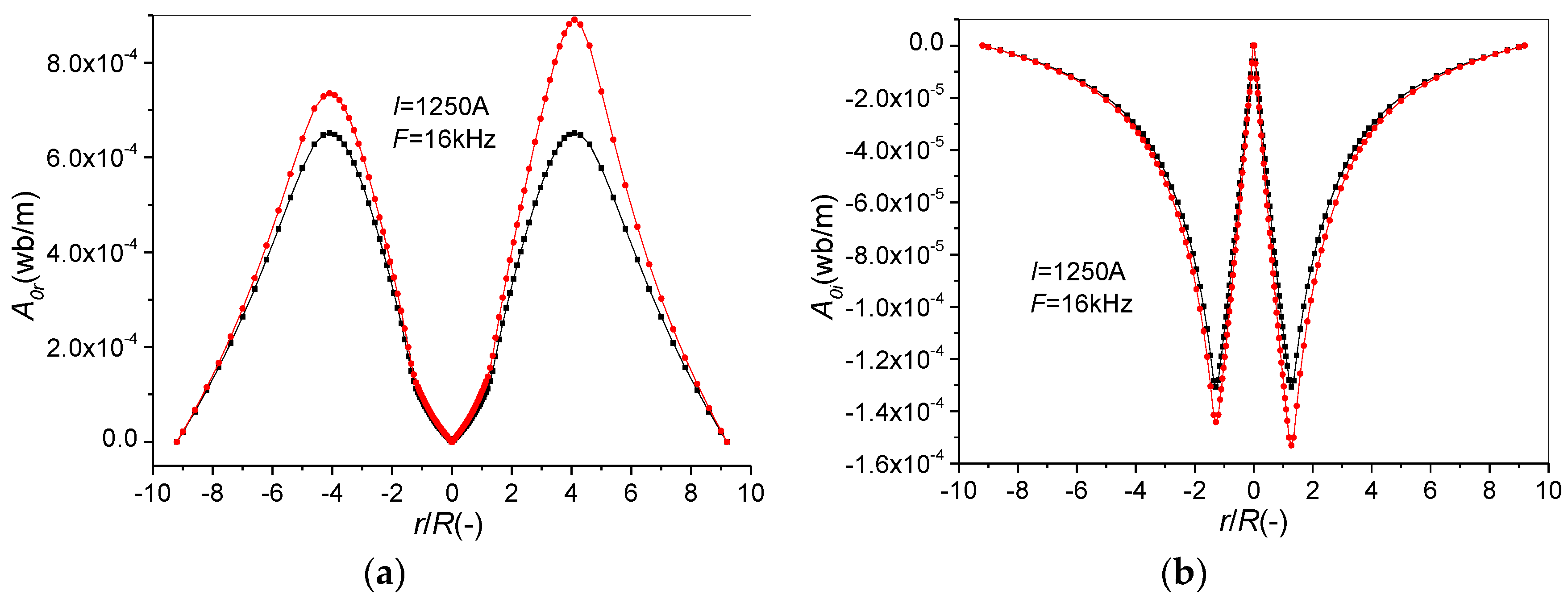
Figure 5 demonstrates the contours of A0r of rz cross section and the iso-surface for axisymmetric coil and spiral coil at I = 1250 A and F = 16 kHz. Axisymmetric A0r are illustrated in Figure 5a for the axisymmetric coil, and it can be seen that it is meaningful 2D axisymmetric model substitute for 3D model for axisymmetric coils. However, it also can be found obviously that A0r is non-axisymmetric as shown in Figure 5b. In addition, as presented in Figure 6, the profile of A0r and A0i in r-direction for axisymmetric and spiral coil also can prove the above viewpoint. Therefore, it demonstrates that the coil structure has a great effect on the electromagnetic field.
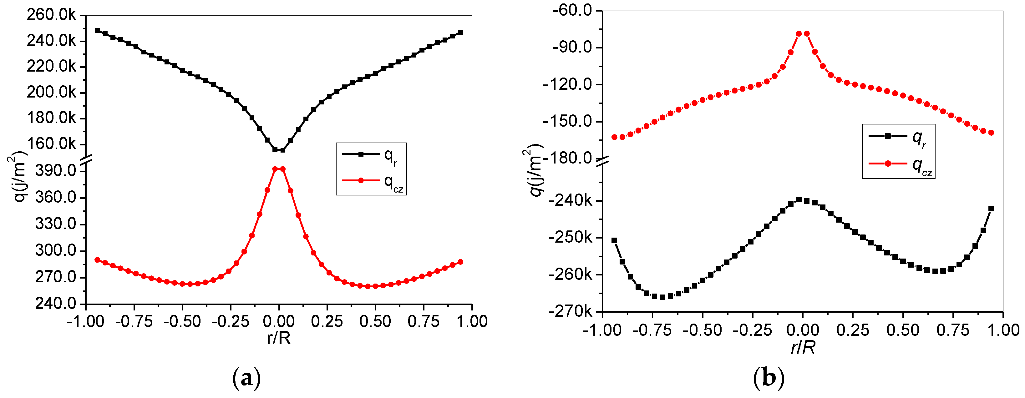
In SiC growth chamber, SiC powder surface, graphite crucible inner surface, and SiC crystal surface radiate strongly. To study the relationship between radiation and conduction heat transfer quantitatively, Figure 7 presents the radiation heat flux (qr) and conduction heat flux (qcz) of SiC powder surface and SiC crystal surface along with radius. It can be seen that: (1) both qr and qcz on SiC powder surface are bigger than 0 as shown in Figure 7a, which illustrates that the surface owns higher temperature and release heat; (2) both qr and qcz on SiC crystal surface are less than 0 as shown in Figure 7b, which illustrates that the surface owns lower temperature and absorption heat; (3) the temperature in the furnace is non-axisymmetric which can be demonstrated by the non-axisymmetric profile of qr and qcz on both surfaces; (4) qr = 160~260 KJ/m2 and qcz = 240~390 J/m2 on powder surface, qr = −160~−80 KJ/m2 and qcz = −270~−240 J/m2 on crystal surface, so qr is about 2~3 orders of magnitude greater than qcz.
Figure 8 shows profiles of temperature of powder surface and crystal surface along with r axis with and without radiation heat transfer, respectively. It can be found that: (1) the average temperature at −0.9 < r/R < 0.9 is 3247.9 K without radiation and it decreases to 2651.7 K with radiation on powder surface; (2) the average temperature is 2212.6 K without radiation and it increases to 2555.3 K with radiation on powder surface; (3) the temperature grandient is 373.1 K/cm without radiation, while it decreases to 34.76 K/cm, which in the suitable temperature ranges (1–50 K/cm) for SiC crystal growth introduced in reference [14]. The above simulation results illustrate that the reasonable temperature difference can be gotten if radiation heat transfer is considered [7] and the radiation is helpful to uniform the temperature field in the chamber.
Figure 9 shows temperature fields of both axisymmetric coil and spiral coil in the furnace at x = 0 cross section, and some similar results with two dimensional axisymmetric model [7,14,18] are obtained: (1) SiC powder and graphite crucible regions own the highest temperature (about 2700~2980 K) which is helpful for SiC to sublimate steadily, this is because the induction coil and induction heat locate in the areas surrounding graphite crucible. The result is coincided with that in the reference [14,18], and the highest growth temperature is about 3000~3100 K on the similar condition; (2) furnace top region owns lower temperature because of continuous heat release from top cooling hole, and then good temperature gradient is formed. Moreover, it can be found obviously that the temperature field of the spiral coil is non-axisymmetric, especially in the powder high temperature region. So it is necessary to simulate the temperature field in the SiC crystal growth furnace by three-dimensional models.
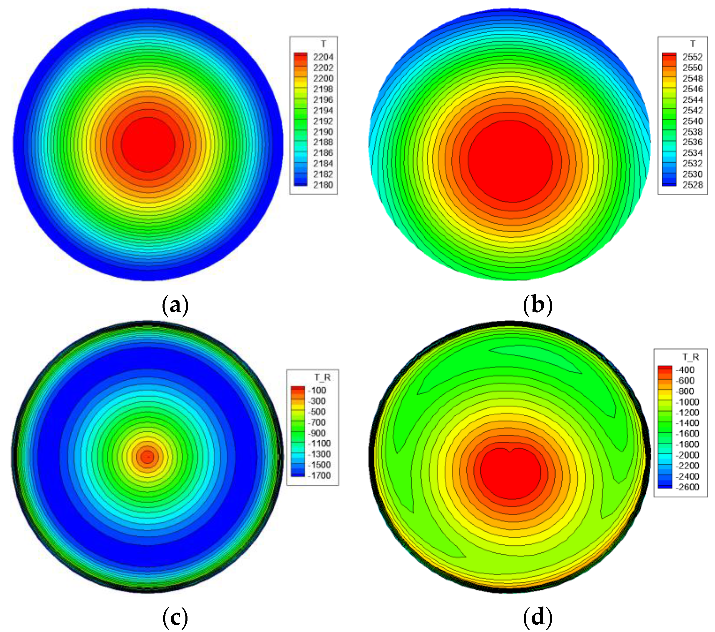
Defects in SiC crystal—such as dislocation, microtubules, etc.—are generated mainly by non-uniform temperature gradient [2,13,19]. Figure 10 presents fields of temperature and temperature gradient (T_R, K/m) in r-direction on rθ cross section in the crystal. A good axisymmetric temperature field is shown in Figure 10a compared with non-axisymmetric temperature field of the spiral coil as shown in Figure 10b. It can be seen from Figure 10b that the highest temperature region deviates from the crystal center, which is as same as the results of Böttcher et al. [13]. The axisymmetric T_R is also gotten for the axisymmetric coil. It is beneficial to grow SiC crystal with fewer defects. As seen from Figure 10d, the T_R is non-axisymmetric for the spiral coil, and the worse T_R are presented in the region far from the center of crystal which may generate more defects.
To study the effect of coil type on the temperature and its gradient evenness (ST, ST_R) quantificationally, the date at r/R = 0.38 are extracted and processed by the sample standard deviation method
{ S = i = 1 n ( T i T ¯ ) 2 n 1 T ¯ = i = 1 n T i n
where Ti is the temperature at mesh cell center, T ¯ is the average temperature, and S means bad temperature or its gradient evenness. For the axisymmetric coil, both ST and ST_R equal 0; for the spiral coil, ST and ST_R are 1.59 and 170.93, respectively. So it is suggested that the coil is closed to axisymmetric structure.

7. Conclusions

A tool to simulate electromagnetic and temperature fields in the SiC crystal growth furnace is developed by using finite volume method with C programing language. LU decomposition algorithm based on GPU technology is developed to accelerate solving process of radiation heat flux, and the least distance method (LDM) is proposed for S2S radiation model to check whether mesh face can see others or not. The electromagnetic and temperature fields are simulated for axisymmetric and spiral coils at I = 1250 A and F = 16 kHz. The radiation and conduction heat transfer are compared with each other quantificationally, and the uniforms of temperature and its gradient are also discussed. The following conclusions are obtained:
(1)
The coil structure has a great effect on temperature field of SiC crystal growth furnace, spiral coil will cause non-axisymmetric temperature field;
(2)
Radiation heat flux is about 2~3 orders of magnitude bigger than conduction heat flux in the growth chamber, and radiation is helpful to make more uniform temperature field and decrease temperature gradient between powder surface and crystal surface;
(3)
The non-axisymmetric temperature and its gradient in the crystal caused by the spiral coil are adverse to grow crystal with fewer defects.

Author Contributions

Chunzhen Yang and Guangxia Liu wrote the paper; Chengmin Chen and Yanjin Hou organized figures; Min Xu and Yongxian Zhang contributed to the paper structure and sentences revise.

Acknowledgments

This work was supported by Shandong Academy of Sciences Foundation (2014QN016, 2016QN005, and 2013QN016).

Conflicts of Interest

The authors declare no conflict of interest.

References

  1. Shiramomo, T.; Gao, B.; Mercier, F.; Nishizawa, S.; Nakano, S.; Kangawa, Y.; Kakimoto, K. Thermodynamical analysis of polytype stability during PVT growth of SiC using 2D nucleation theory. J. Cryst. Growth 2012, 352, 177–180. [Google Scholar] [CrossRef]
  2. Su, J.; Chen, X.; Li, Y. Numerical design of induction heating in the PVT growth of SiC crystal. J. Cryst. Growth 2014, 401, 128–132. [Google Scholar] [CrossRef]
  3. Hofmann, D.; Heinze, M.; Winnacker, A.; Durst, F.; Kadinski, L.; Kaufmann, P.; Makarov, Y.; Schäfer, M. On the sublimation growth of SiC bulk crystals: Development of a numerical process model. J. Cryst. Growth 1995, 146, 214–219. [Google Scholar] [CrossRef]
  4. Hofmann, D.; Bickermann, M.; Eckstein, R.; Kölbl, M.; Müller, S.G.; Schmitt, E.; Weber, A.; Winnacker, A. Sublimation growth of silicon carbide bulk crystals: Experimental and theoretical studies on defect formation and growth rate augmentation. J. Cryst. Growth 1999, 198–199 Pt 2, 1005–1010. [Google Scholar] [CrossRef]
  5. Liu, X.; Chen, B.; Song, L.; Shi, E.; Chen, Z. The behavior of powder sublimation in the long-term PVT growth of SiC crystals. J. Cryst. Growth 2010, 312, 1486–1490. [Google Scholar] [CrossRef]
  6. Selder, M.; Kadinski, L.; Durst, F.; Straubinger, T.; Hofmann, D. Numerical simulation of global heat transfer in reactors for SiC bulk crystal growth by physical vapor transport. Mater. Sci. Eng. B 1999, 61–62, 93–97. [Google Scholar] [CrossRef]
  7. Chen, Q.; Zhang, H.; Ma, R.; Prasad, V.; Balkas, C.M.; Yushin, N.K. Modeling of transport processes and kinetics of silicon carbide bulk growth. J. Cryst. Growth 2001, 225, 299–306. [Google Scholar] [CrossRef]
  8. Klein, O.; Philip, P. Transient temperature phenomena during sublimation growth of silicon carbide single crystals. J. Cryst. Growth 2003, 249, 514–522. [Google Scholar] [CrossRef]
  9. Klein, O.; Philip, P. Transient numerical investigation of induction heating during sublimation growth of silicon carbide single crystals. J. Cryst. Growth 2003, 247, 219–235. [Google Scholar] [CrossRef]
  10. Lu, J.; Zhang, Z.; Chen, Q. Numerical simulation of the flow field and concentration distribution in the bulk growth of silicon carbide crystals. J. Cryst. Growth 2006, 292, 519–522. [Google Scholar] [CrossRef]
  11. Chen, Q.; Yan, J.; Prasad, V. Application of flow-kinetics model to the PVT growth of SiC crystals. J. Cryst. Growth 2007, 303, 357–361. [Google Scholar] [CrossRef]
  12. Inui, F.; Gao, B.; Nakano, S.; Kakimoto, K. Numerical analysis of the velocity of SiC growth by the top seeding method. J. Cryst. Growth 2012, 348, 71–74. [Google Scholar] [CrossRef]
  13. Böttcher, K.; Cliffe, K.A. Three-dimensional thermal stresses in on-axis grown SiC crystals. J. Cryst. Growth 2005, 284, 425–433. [Google Scholar] [CrossRef]
  14. Chen, Q.; Zhang, H.; Prasad, V.; Balkas, C.M.; Yushin, N.K.; Wang, S. Kinetics and modeling of sublimation growth of silicon carbide bulk crystal. J. Cryst. Growth 2001, 224, 101–110. [Google Scholar] [CrossRef]
  15. Bogdanov, M.V.; Galyukov, A.O.; Karpov, S.Y.; Kulik, A.V.; Kochuguev, S.K.; Ofengeim, D.K.; Tsiryulnikov, A.V.; Ramm, M.S.; Zhmakin, A.I.; Makarov, Y.N. Virtual reactor as a new tool for modeling and optimization of SiC bulk crystal growth. J. Cryst. Growth 2001, 225, 307–311. [Google Scholar] [CrossRef]
  16. Geiser, J.; Klein, O.; Philip, P. Transient numerical study of temperature gradients during sublimation growth of SiC: Dependence on apparatus design. J. Cryst. Growth 2006, 297, 20–32. [Google Scholar] [CrossRef]
  17. Xue, S.; Proulx, P.; Boulos, M.I. Extended-field electromagnetic model for inductively coupled plasma. J. Phys. D Appl. Phys. 2001, 34, 1897–1906. [Google Scholar] [CrossRef]
  18. Chen, Q.; Zhang, H.; Prasad, V. Heat transfer and kinetics of bulk growth of silicon carbide. J. Cryst. Growth 2001, 230, 239–246. [Google Scholar] [CrossRef]
  19. Chen, X.; Nishizawa, S.; Kakimoto, K. Numerical simulation of a new SiC growth system by the dual-directional sublimation method. J. Cryst. Growth 2010, 312, 1697–1702. [Google Scholar] [CrossRef]
Figure 1. Silicon carbide crystal growth furnace and its three-dimensional mesh. (a) Physical model for electromagnetic field; (b) physical model for temperature field; (c) mesh for the furnace.
Applsci 08 00705 g001
Figure 2. Diagram and flowchart for visible surface to surface radiation model. (a) Diagram; (b) flowchart.
Applsci 08 00705 g002
Figure 3. Visible regions of grids located on growth chamber. (a) Grid 1 on SiC powder surface; (b) calculated visible region for grid 1; (c) grid 2 on graphite crucible inner surface; (d) calculated visible region for grid 2.
Applsci 08 00705 g003
Figure 4. A0 and T profiles in r-direction for different meshes. (a) real part of magnetic potential, A0r; (b) imaginary part of magnetic potential, A0i; (c) temperature, T.
Applsci 08 00705 g004
Figure 5. Contours of A0r for axisymmetric and spiral coils at I = 1250 A and F = 16 kHz. (a) axisymmetric coil; (b) spiral coil.
Applsci 08 00705 g005
Figure 6. Profiles of A0r and A0i in r-direction for axisymmetric and spiral coil at I = 1250 A and F = 16 kHz. (a) A0r; (b) A0i.
Applsci 08 00705 g006
Figure 7. Radiation and conduction heat flux on surfaces of SiC powder and crystal. (a) SiC powder surface; (b) SiC crystal surface.
Applsci 08 00705 g007
Figure 8. Temperature profiles on SiC powder surface and SiC crystal surface along with r-direction.
Applsci 08 00705 g008
Figure 9. Temperature field at I = 1250 A and F = 16 kHz. (a) Axisymmetric coil; (b) spiral coil.
Applsci 08 00705 g009
Figure 10. Temperature and its gradient fields in SiC crystal. (a) temperature for axisymmetric coil; (b) temperature for spiral coil; (c) temperature gradient for axisymmetric coil; (d) temperature gradient for spiral coil.
Applsci 08 00705 g010
Table 1. Physical properties of materials of SiC growth furnace.
Material NameDensity (ρ)
kg/m3
Heat Capacity (cp)
J/(kg·K)
Conductivity (λ)
W/(m·K)
SiC crystal3140.0 1 3.9 × 10 3 T 3.17 + 1.83 × 10 3 T 0.11 61100 T 115
Graphite crucible1750.0 37.7 e 1.96 × 10 4 T 1 441.12 T 2.3 + 7.97 × 10 4 T 6.65 × 10 2
Felt170.02100.0 { 8.17 × 10 2 + 2.49 × 10 4 T , T 1473 K 4.19 × 10 4 T 0.67 , T > 1473 K
Table 2. Time consumed to solve AC = B by CPU and GPU with different mesh number.
CaseMesh NumberNumber of Radiation SurfaceCPU Time (s)GPU Time (s)ΔT (K/cm)
136 × 51 × 7723042557137.36
245 × 43 × 71432019719734.88
356 × 43 × 715184335520334.76
474 × 43 × 71691214,42124735.15
Table 3. Mesh number for electromagnetic and temperature field (Nθ × Nr × Nz).
No.Electromagnetic FieldTemperature Field
136 × 51 × 7736 × 51 × 77
245 × 64 × 13145 × 43 × 71
356 × 64 × 13156 × 43 × 71
474 × 64 × 13174 × 43 × 71