1. Introduction
A quadrature sinusoidal oscillator is a very important active element for communication, instrumentation, and measurement systems, and can be employed in a quadrature mixer and a single-sideband modulator of telecommunications [
1,
2]. In communication systems, a sinusoidal oscillator can generate an amplitude-controllable sinusoidal signal, which can be used to apply the carrier signal for amplitude modulation (AM) and amplitude shift keying (ASK) signal systems [
3]. Recently, current conveyors are receiving considerable attention due to their potential advantages, such as inherently wide bandwidth, high slew-rate, good linearity, wide dynamic range, simple circuitry, and low power consumption [
4]. This interesting active element, based on second-generation current conveyor transconductance amplifiers (CCIITA) [
5], has been introduced to provide new possibilities in the realization of a class of analog signal processing circuits. This CCIITA can provide flexibility in operating both current and voltage modes, and can enable a variety of circuit designs and provides electronic tuning ability through its transconductance gain,
gm. However, the CCIITA cannot control the parasitic resistance,
RX, at
X port. Hence, when the CCIITA is used in some circuits, it must unavoidably require some external passive components, especially with the resistors. In contrast, the introduced current-controlled current conveyor transconductance amplifier (CCCCTA) [
5,
6] has two electronically adjustable ports, whereas the CCIITA has only one electronically adjustable port. The parasitic resistance,
RX, at current input port of the CCCCTA can be adjusted by an input bias current, which does not require a resistor in practical applications. Intuitively, the CCCCTA is a versatile active building block, which provides the possibility of utilizing its transconductance gain,
gm, and its equivalent input resistance, namely parasitic resistance,
RX, to create a resistorless oscillator scheme. The multiple current output terminals of the CCCCTA can be easily obtained by adding additional current mirrors at these output terminals.
Electronically tunable active components are receiving more attention as traditional electronic components may have deviations in fine-tuning the tolerances of the electronic components [
7]. The electronically tunable active components of the previous second-order oscillators include second generation current controlled conveyors (CCCIIs) [
8,
9]; operational transconductance amplifiers (OTAs) [
10]; current differencing buffered amplifiers (CDBAs) [
11,
12]; the CCIITA [
13]; current differencing transconductance amplifiers (CDTAs) [
14,
15,
16,
17,
18,
19]; multiple-output current controlled current conveyor transconductance amplifiers (MO-CCCCTAs) [
20]; and voltage differencing transconductance amplifiers (VDTAs) [
21]. These circuits were used to design the second-order quadrature current outputs, quadrature voltage outputs, or both quadrature current and voltage outputs. In addition to all of the above second-order quadrature oscillators, several third-order quadrature oscillators have also been proposed [
22,
23,
24,
25,
26,
27,
28,
29,
30,
31,
32].
The third-order oscillators have higher accuracy, higher quality factor, and lower harmonic distortion than the second-order oscillators [
22,
23]. However, the third-order oscillator in
Figure 7 of Reference [
22] uses three OTAs and three grounded capacitors. The third-order oscillator in Reference [
23] uses four multiple-output second-generation current-controlled conveyors (MO-CCCIIs) and three grounded capacitors. The third-order oscillator in
Figure 1 of Reference [
24] uses three second-generation current conveyors (CCIIs), five grounded resistors and three capacitors. The third-order oscillator in Reference [
25] uses two MO-CCCCTAs and three grounded capacitors. The third-order oscillator in
Figure 3 of Reference [
26] uses three voltage controlled differential voltage current conveyors (VC-DVCCs) and three grounded capacitors. The third-order oscillator in Reference [
27] uses three MO-CCCIIs and three grounded capacitors. The third-order oscillator in Reference [
28] uses three multiple-output current differencing transconductance amplifiers (MO-CDTAs) and three grounded capacitors. Although the third-order oscillator in Reference [
29] uses two multiple-output second-generation current conveyors (MO-CCIIs), three resistors, and three grounded capacitors, one of the resistors is a floating connection. The third-order oscillator in Reference [
30] uses three multiple-output differential voltage current conveyors (MO-DVCCs), three resistors, and three grounded capacitors; however, one of the resistors is also a floating connection. The oscillator in
Figure 2 of Reference [
31] uses three operational transresistance amplifiers (OTRAs), four resistors and three capacitors; however, not all of the resistors and capacitors are grounded.
In 2015, two new third-order quadrature oscillators were proposed [
32], which employed two multiple-output differential voltage current conveyor transconductance amplifiers (MO-DVCCTAs), one/two resistors, and three grounded capacitors. However, these circuits [
22,
23,
24,
25,
26,
27,
28,
29,
30,
31,
32] suffered from one or more of the following drawbacks: (i) the inclusion of three/four active components [
22,
23,
24,
26,
27,
28,
30,
31]; (ii) the lack of both a voltage-mode and current-mode quadrature oscillator in one circuit topology [
22,
23,
24,
25,
31]; (iii) the lack of a resistorless oscillator [
24,
29,
30,
31,
32]; (iv) the lack of an independently electronically tunable for the oscillation condition and frequency [
22,
24,
30,
32]; (v) the lack of amplitude-controllable for output current signal [
22,
23,
24,
25,
26,
27,
28,
29,
30,
31,
32]; and (vi) the lack of quadrature voltage outputs, quadrature current outputs, and a high-impedance amplitude-controllable current output in one circuit topology [
22,
23,
24,
25,
26,
27,
28,
29,
30,
31,
32], especially, the electronically controllable amplitude of the sinusoidal current output signal that can be easily used in AM/ASK systems.
In this paper, a new approach to realize third-order quadrature oscillators using a lossy integrator and two lossless integrators is proposed. The proposed third-order quadrature resistorless oscillator employs two MO-CCCCTAs and three grounded capacitors. The proposed third-order quadrature oscillator has the following seven advantages simultaneously: (i) it contains only two active components and three grounded capacitors; (ii) it has both voltage-mode and current-mode third-order sinusoidal quadrature oscillator in the same topology; (iii) it achieves quadrature voltage outputs, quadrature current outputs, and a high-impedance amplitude-controllable current output in one circuit topology; (iv) it has independent electronically tunable characteristics for the condition of oscillation (CO) and the frequency of oscillation (FO); (v) it provides a high-impedance current output of adjustable magnitude, without effecting the CO and FO and is suitable for AM/ASK modulations; (vi) it uses only grounded capacitors; and (vii) it holds low active and passive sensitivity performances.
Table 1 and
Table 2 compare the main features of the proposed circuit with previous third-order sinusoidal oscillators [
22,
23,
24,
25,
26,
27,
28,
29,
30,
31,
32].
3. Circuit Descriptions
The CCCCTA is an active building block, which is useful in simplifying the circuit design. The CCCCTA device integrates a CCCII and an OTA into a versatile component to facilitate the implementation of analog signal-processing circuits. The CCCCTA does not need a resistor in practical applications, as its transconductance gain,
gm, and parasitic resistance,
RX, are electronic adjustable.
Figure 2 shows the symbol of a multiple-output CCCCTA (MO-CCCCTA) [
33]. The MO-CCCCTA properties can be expressed as
VX =
VY +
IXRX,
IZ =
IZC1 =
IZC2 =
IX and
IO1 =
IO2 =
gmVZ, where
RX is the parasitic resistance of the
X-terminal, and
gm is the transconductance gain of the MO-CCCCTA. The bias currents,
IS and
IB, of MO-CCCCTA can control the parasitic resistance,
RX, and the transconductance gain,
gm, respectively [
33,
34].
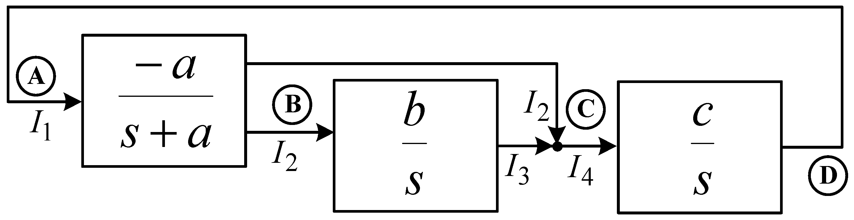
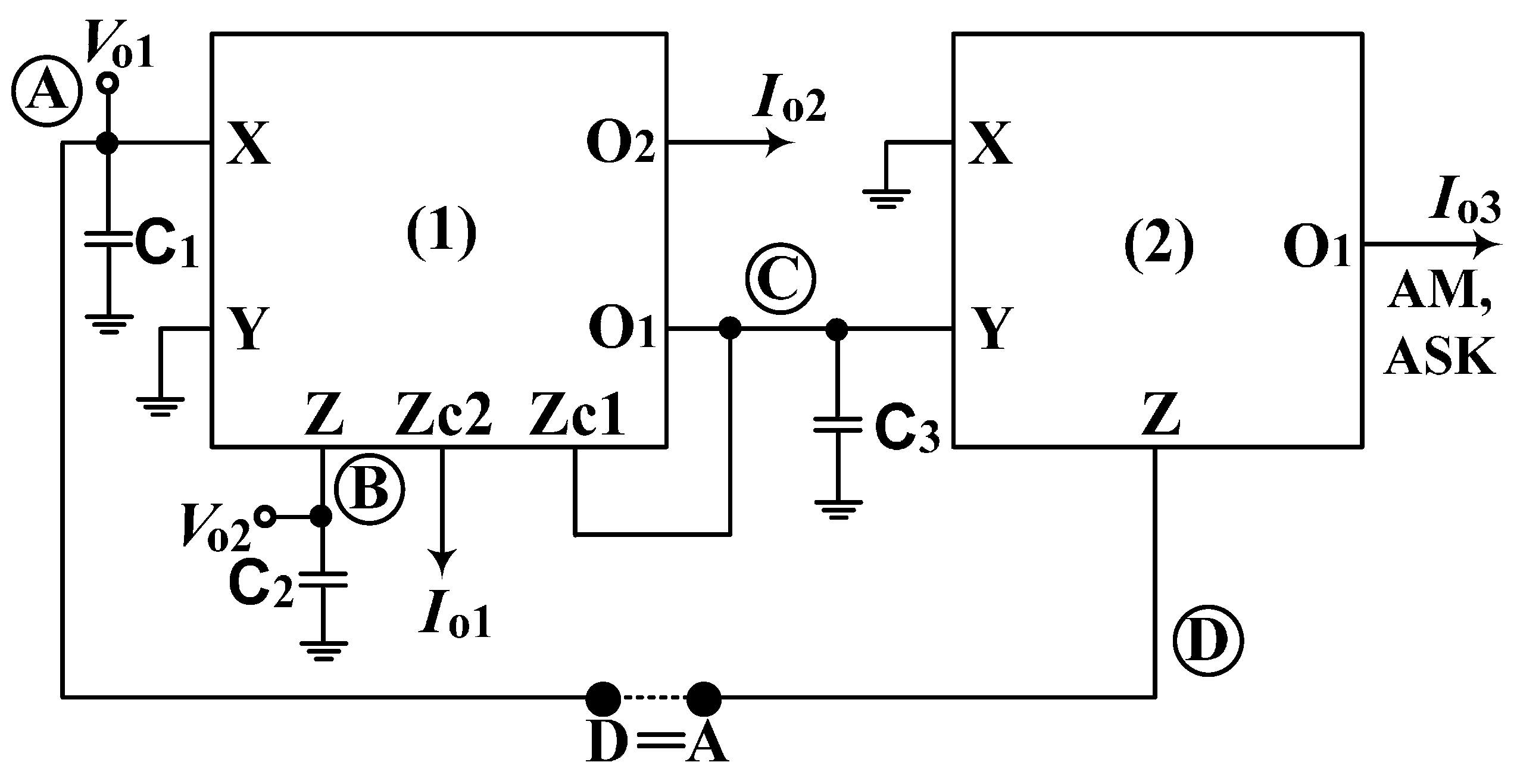
Figure 3 shows the proposed schematic of the resistorless third-order quadrature oscillator, which consists of two MO-CCCCTAs and three grounded capacitors. The only grounded capacitors without a resistor structure in the proposed circuit are easily integrated into a single chip. In
Figure 3, the transfer function,
B/
A, realizes a current-mode lossy integrator, and the transfer functions,
C/
B and
D/
C, realize two current-mode lossless integrators.
Let
D =
A, and the close-loop circuit analysis provides the following system characteristic equation.
and the CO and FO can be obtained as:
As indicated by Equations (9) and (10), the CO can be adjusted by
RX1 without disturbing the FO, and the FO can be controlled by
RX2 without affecting the CO. In other words, the CO and FO are controlled independently by the bias currents,
IS1 and
IS2, respectively. As the parasitic resistances,
RX1 and
RX2, of the MO-CCCCTA can be electronically controlled by
IS1 and
IS2, respectively, both the CO and FO are independently and electronically controllable. In a steady state, the two voltage outputs and two current outputs in
Figure 3 are:
where
, and
.
Equation (11) shows that the proposed circuit can obtain the quadrature voltage outputs and the quadrature current outputs simultaneously. The magnitude ratios of the quadrature voltage outputs and the quadrature current outputs are the function of the operating frequency. Thus, the value of RX2 will affect the oscillation frequency and the magnitude ratios of the generated quadrature signals. However, this problem can be solved by using C1 = C2 = C3, RX1 = RX2, and letting the product gm1RX1 = 1. Subsequently, the amplitude of voltages and currents in Equation (11) are equal and ensure k1 = k2 = 1.
The output current,
Io3, can be given as follows:
where the
gm2 of the second MO-CCCCTA can be independently tuned by the bias current,
IB2. This means that the
gm2-value can be tuned by
IB2, without disturbing the CO and FO. Thus, if a modulating signal is applied to
IB2, then the AM/ASK signals can be obtained from
Io3.
From Equation (11), the magnitude of
Vo2 and
Vo1 or
Io2 and
Io1 is dependent on the factor
k1 or
k2. Therefore, the mechanism of amplitude limitation will depend on the factors
k1 and
k2. For complementary metal oxide semiconductor (CMOS) implementation of CCCCTA [
34], the
RX and
gm are written as:
where
,
.
RX is the parasitic resistance of the
X-terminal and
gm is the transconductance gain of the CCCCTA. Here
k is the physical transconductance parameter of the MOS transistor.
IS and
IB are the bias current used to control the parasitic resistance and transconductance gain, respectively. In other words, the variation of CCCCTA bias current range will limit the stability of the output amplitude.
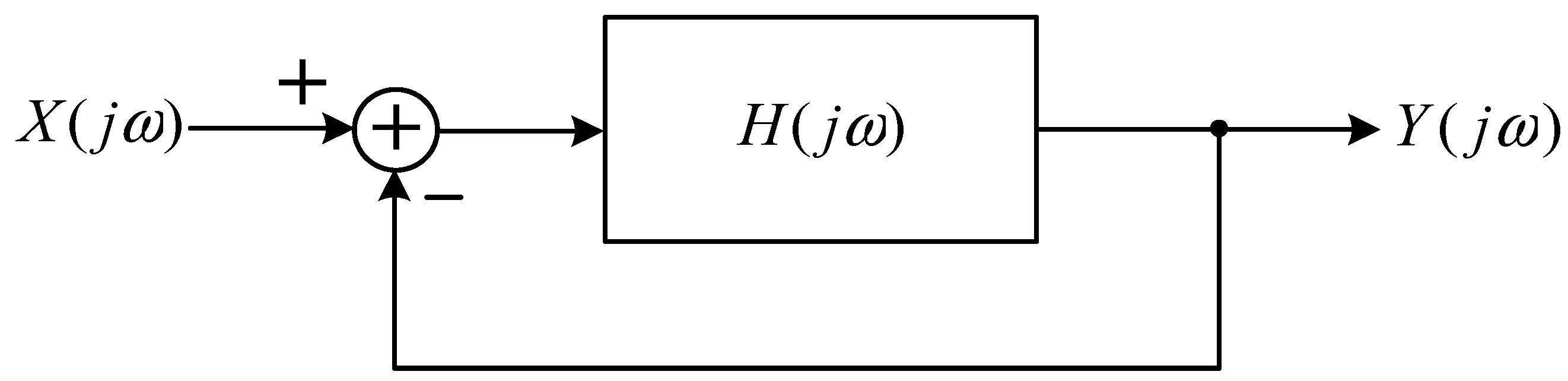
4. Phase Noise and Phase Error Analysis
The phase noise, which are the important performance parameters of an oscillator, can be calculated by the method outlined in Reference [
35] and can be represented in the block diagram of
Figure 4. The spectral density of the phase noise is defined in Reference [
35].
where
ωo is oscillation frequency and
ω =
ωo + Δ
ω is carrier frequency approximation.
If
, then:
Substitute Equation (15) into Equation (14) and get:
The phase noise of the proposed circuit can be obtained by Equations (14)–(16).
Quadrature oscillators are widely used in communication systems due to its in-phase and quadrature phase signals, which deviate from 90°. Therefore, the quadrature phase accuracy between the two output signals should be reasonable. Generally, the in-phase and quadrature phase expressions of the quadrature oscillator signals can be written as:
where
ω is the oscillation frequency and
ϕ is the phase deviation from the quadrature signal.
VI(
t) is the in-phase signal and
VQ(
t) is the quadrature phase signal. The phase error of the proposed circuit can be obtained by Equations (17)–(19).
5. Non-Ideal Discussion
The terminal voltage and current relationships of the non-ideal
ith MO-CCCCTA can be rewritten as
VXi =
βiVYi +
IXiRXi,
IZi =
αiIX,
IZC1i =
ηiIXi,
IO1i =
γigmiVZi and
IO2i =
λigmiVZi for
i = 1, 2, where
βi,
αi.
γi, ηi and
λi represent the tracking errors of the MO-CCCCTA voltage and current, respectively [
20]. The characteristic equation of the proposed circuit in
Figure 3 can be rewritten as:
In this case, the CO and FO of the non-ideal oscillator can be expressed as:
The active and passive sensitivities of the non-ideal oscillator parameters are shown as:
From Equation (23), the active and passive sensitivities are equal to 0.5, which satisfy the sensitivity performance of the circuit.
The parasitic terminal impedances of the
ith non-ideal MO-CCCCTA are (
RYi//
CYi) of terminal
Yi, (
RZi//
CZi) of terminal
Zi, (
RZC1i//
CZC1i) of terminal
ZC1i, (
RZC2i//
CZC2i) of terminal
ZC2i, (
RO1i//
CO1i) of terminal
O1i, and (
RO2i//
CO2i) of terminal
O2i [
20,
33]. The
X,
Z, and
O1 of the first MO-CCCCTA terminals connect to the external
C1,
C2 and
C3 capacitors in parallel, respectively, as shown in
Figure 3. If
C1 >>
CZ2,
C2 >>
CZ1 and
C3 >> (
CO11 +
CY2 +
CZC11), the effects of the parasitic capacitances,
CZ2,
CZ1 and
CO11, can be ignored. Hence, to minimize the effects of the MO-CCCCTA parasitic terminal impedances, the external capacitor values should be restricted by
6. Simulation Results
To verify the theoretical analysis of the proposed circuit, an H-Spice simulation with Taiwan Semiconductor Manufacturing Company (TSMC) 0.18 µm process was performed.
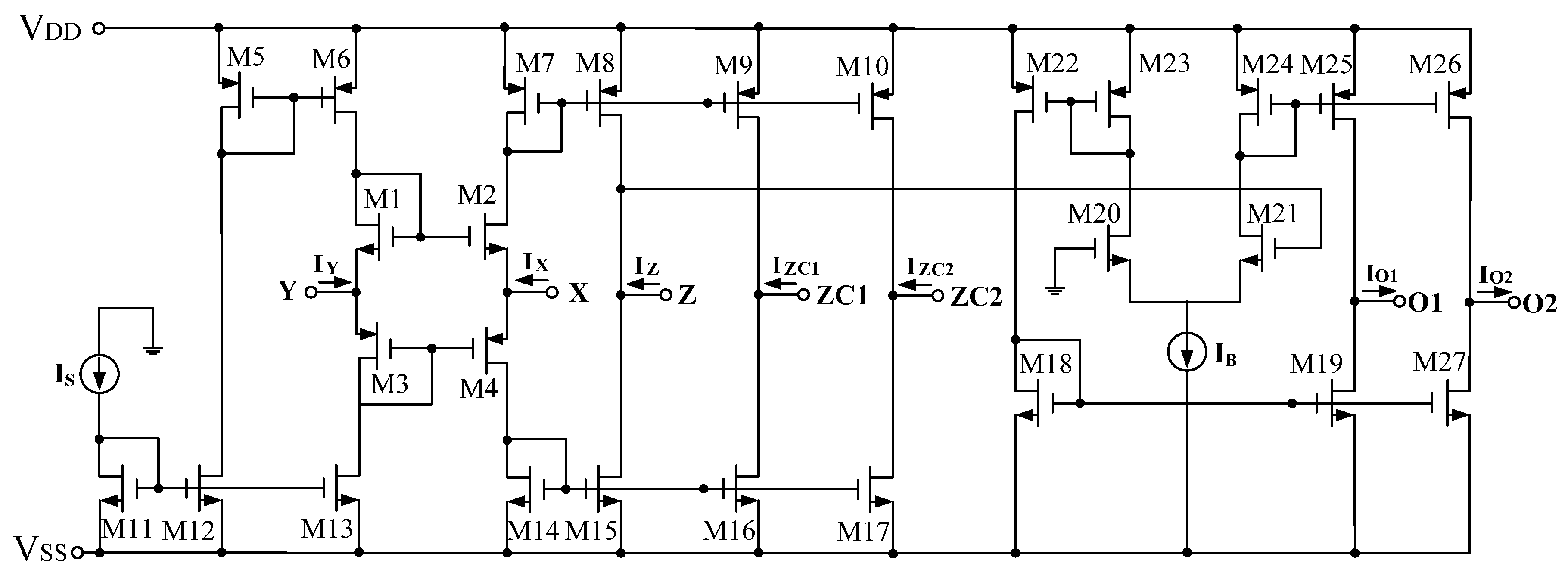
Figure 5 shows the CMOS schematic of a MO-CCCCTA [
34], where the multiple outputs are multiple current mirrors. The aspect ratios (
W/
L) of the MOS transistors of
Figure 5 are given in
Table 3. The supply voltages are
VDD = −
VSS = 0.9 V. In order to get the
fo ≅ 2.12 MHz oscillation frequency of the sinusoidal output waveforms, the values of the active and passive components have been chosen as
gm1 =
gm2 = 133.33 µA/V (
IB = 42.9 µA);
RX1 =
RX2 = 7.5 kΩ (
IS = 3.96 µA);
C1 = 10.1 pF; and
C2 =
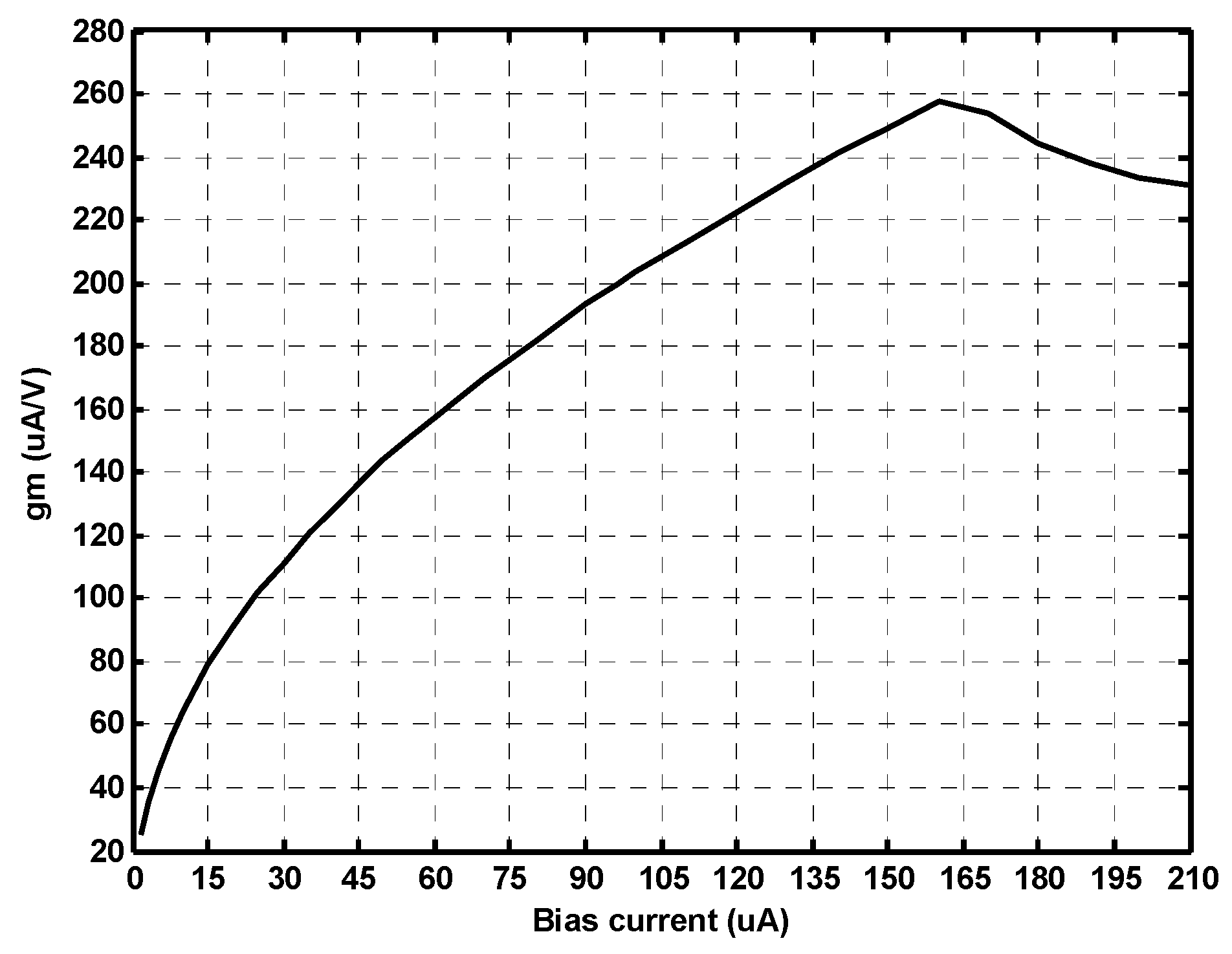
C3 = 10 pF. The variation of the transconductance value changes
IB from 1.5 μA to 210 μA as depicted in
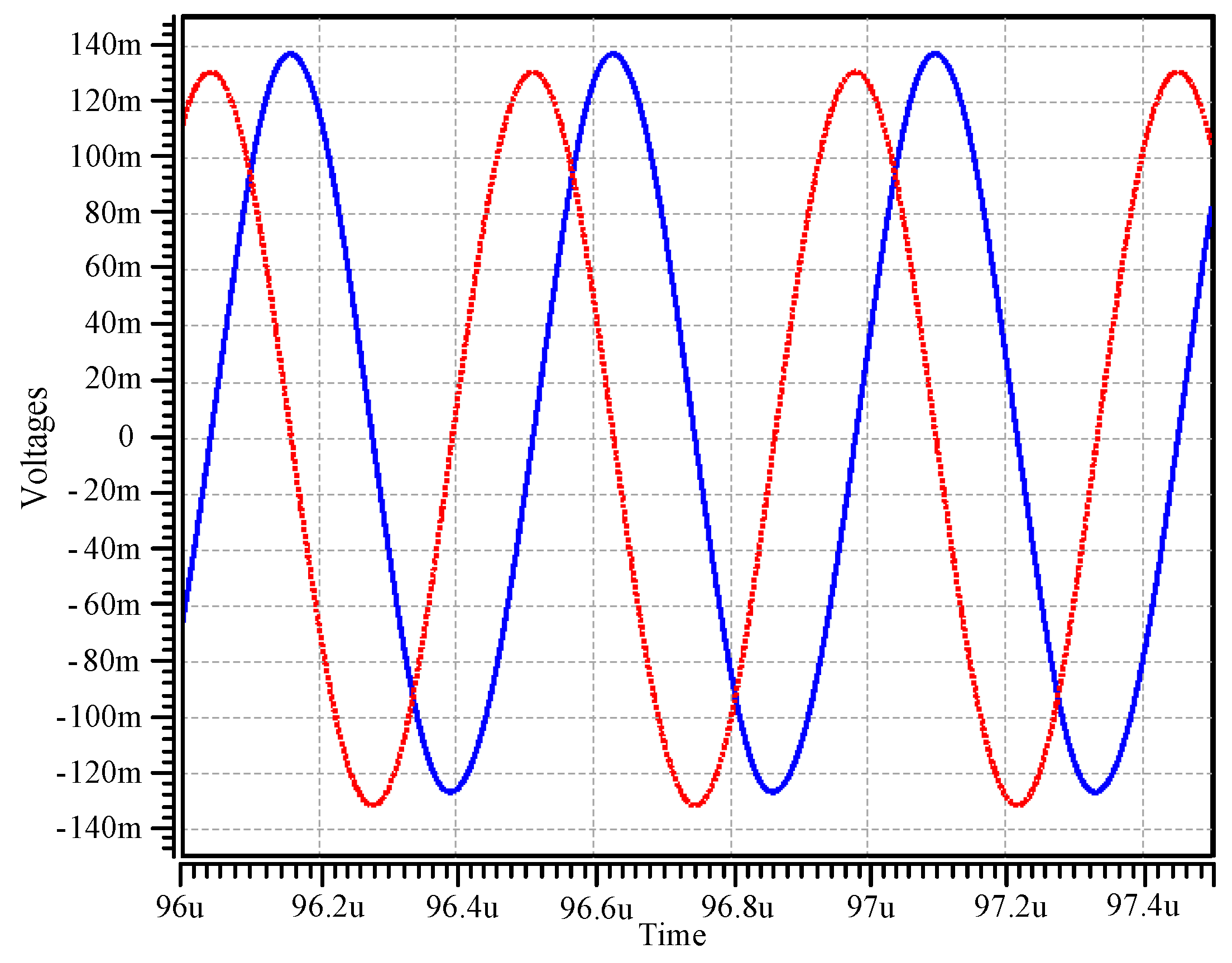
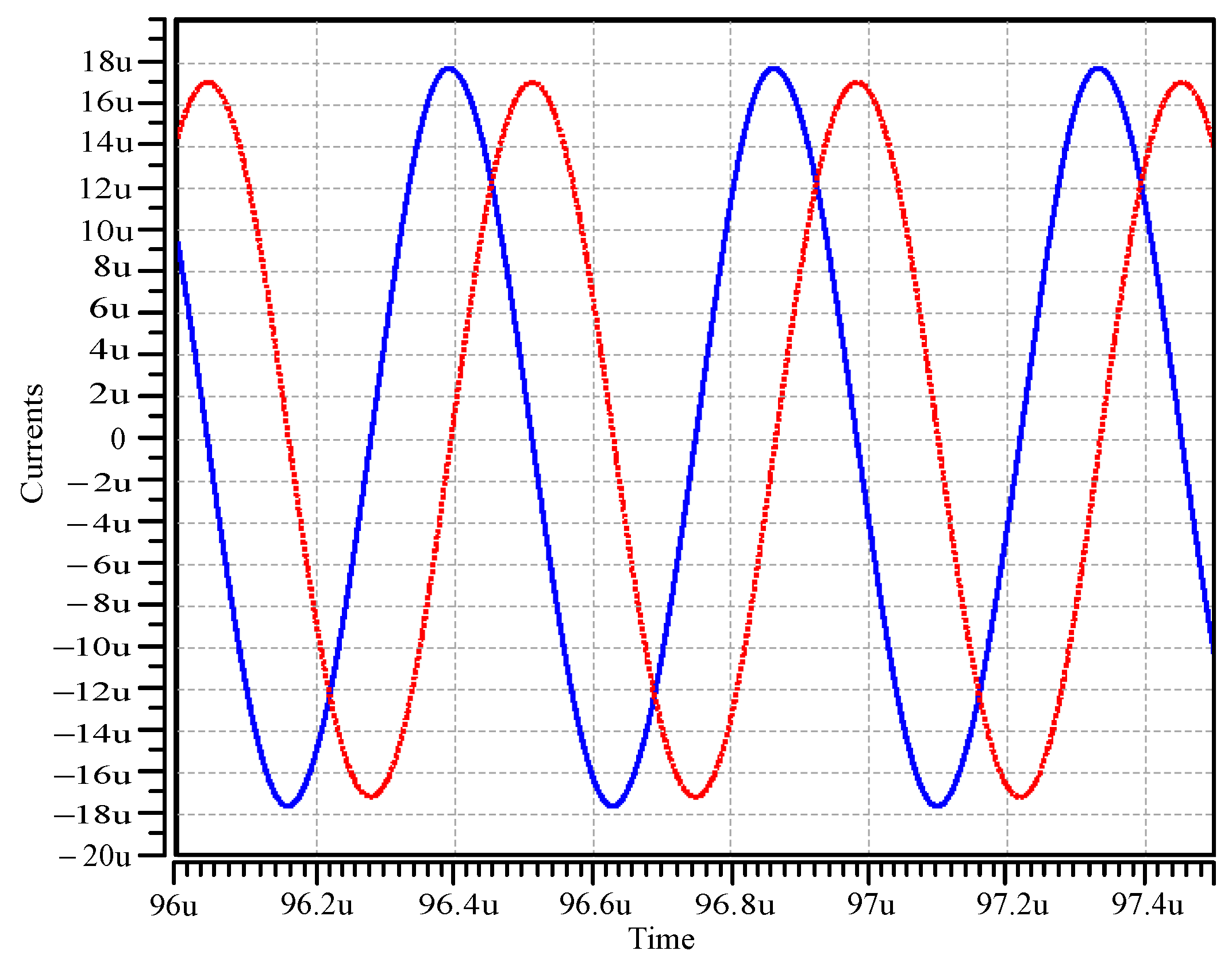
Figure 6. When the bias current is larger than 160 μA, the transconductance gain is decreased as the transistors (M20, M21) enter the linear region from a saturation region. The maximum transconductance gain is approximately 256 µA/V. In other words, when the bias current is larger than 160 μA, the internal construction transistors of the MO-CCCCTA operates in the linear region, which will result in the distortion of the output swing. The steady state output waveforms of the quadrature voltages are shown in
Figure 7 and the quadrature currents are shown in
Figure 8. The oscillation frequency,
fo, of the simulation results is equal to 2.11 MHz, which is consistent with the theoretical analysis. The total harmonic distortion (THD) analysis of the
Vo1,
Vo2,
Io1 and
Io2 are summarized in
Table 4,
Table 5,
Table 6 and
Table 7, respectively. Furthermore, the output current,
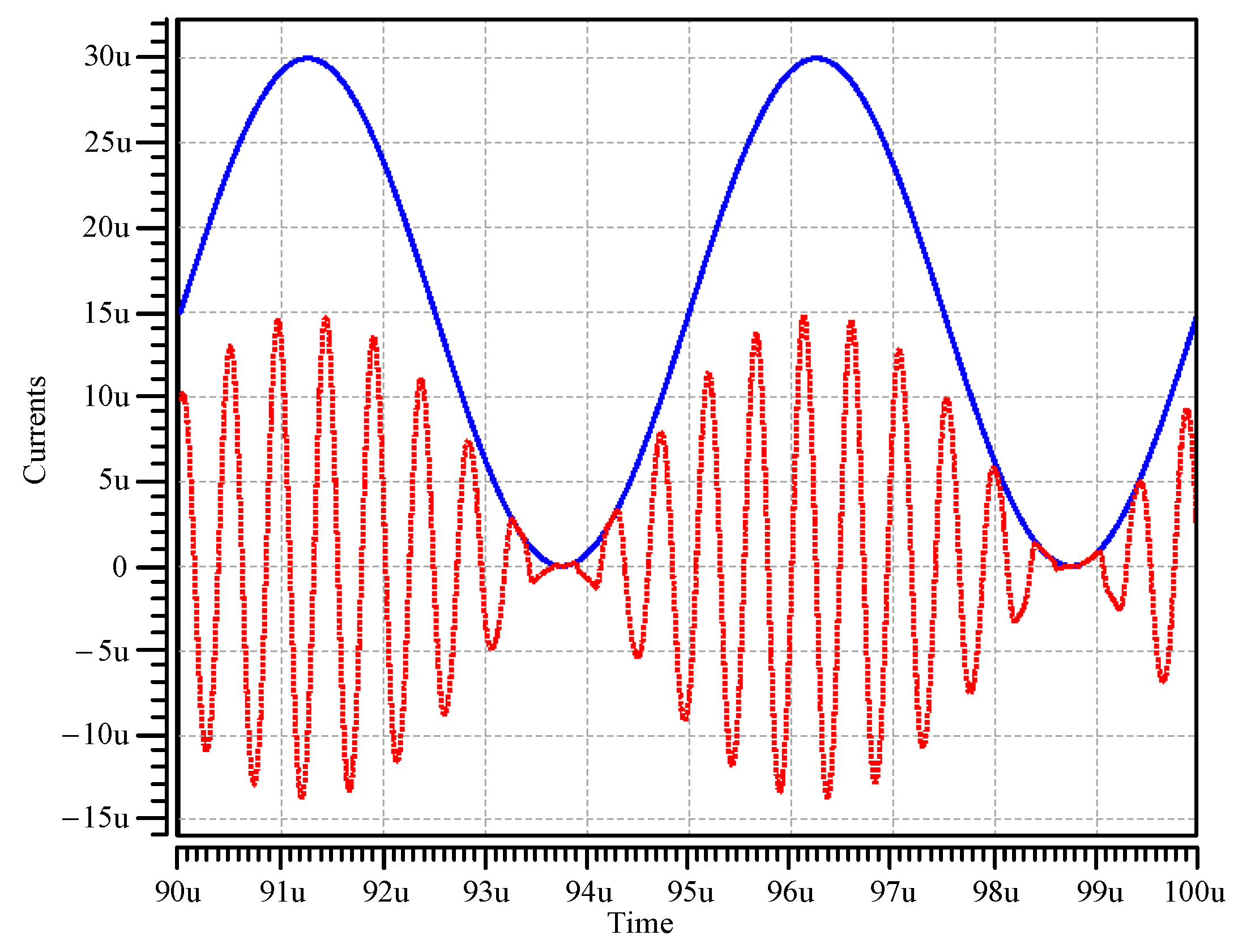
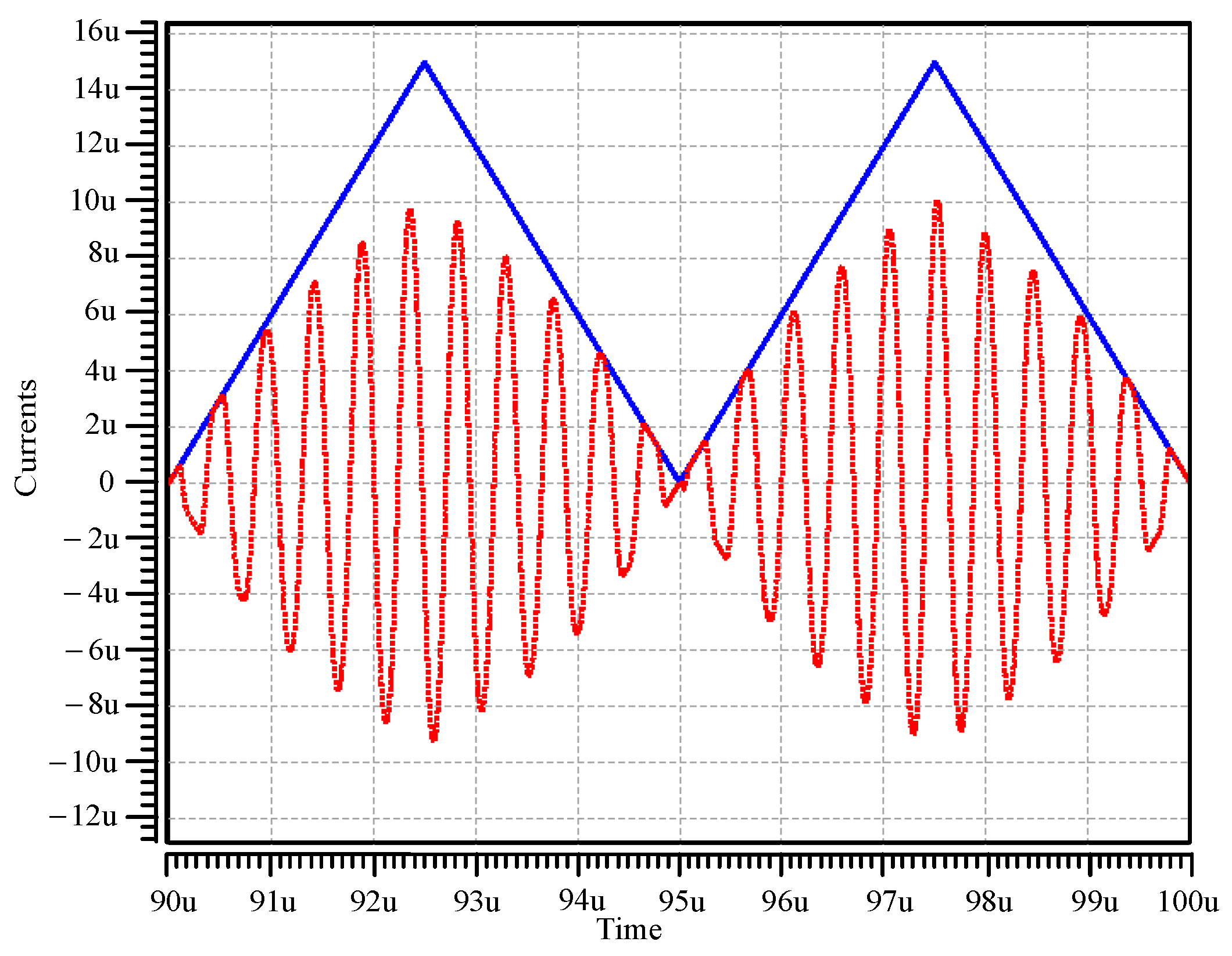
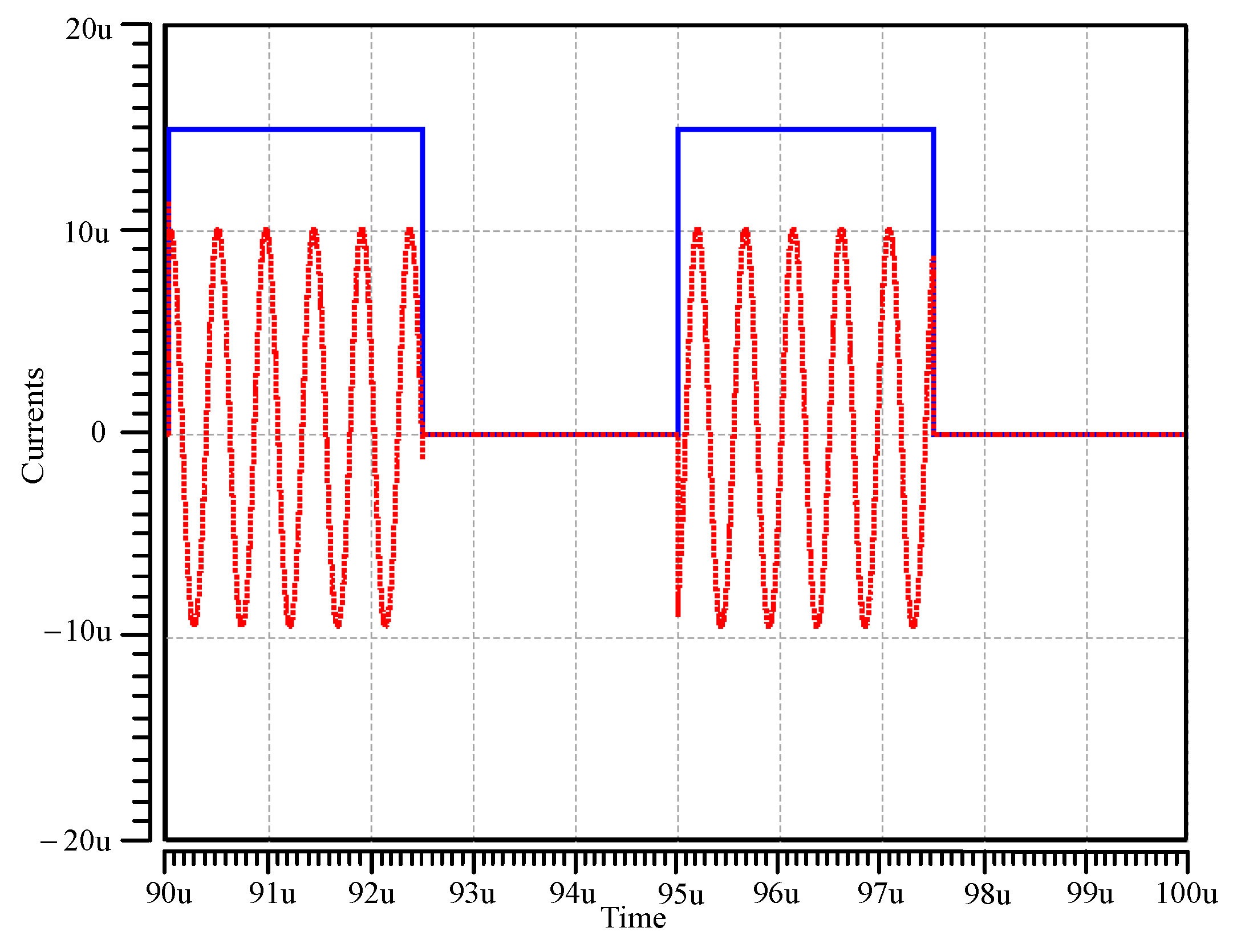
Io3, can be used as an AM or ASK signal generator, when the amplitude of the input bias current,
IB2, is applied to a sinusoidal signal, a triangular signal, or a pulse signal. Thus, the proposed oscillator can generate either AM or ASK signals without additional elements.
Figure 9 and
Figure 10 show the simulated results of the proposed circuit serving as an AM signal generator, when the input bias current,
IB2, is applied to a sinusoidal signal or a triangular signal with a 200-kHz frequency.
Figure 11 shows the simulated results of the proposed circuit serving as an ASK signal generator when the input bias current,
IB2, is applied to a pulse signal with a 200-kHz frequency.
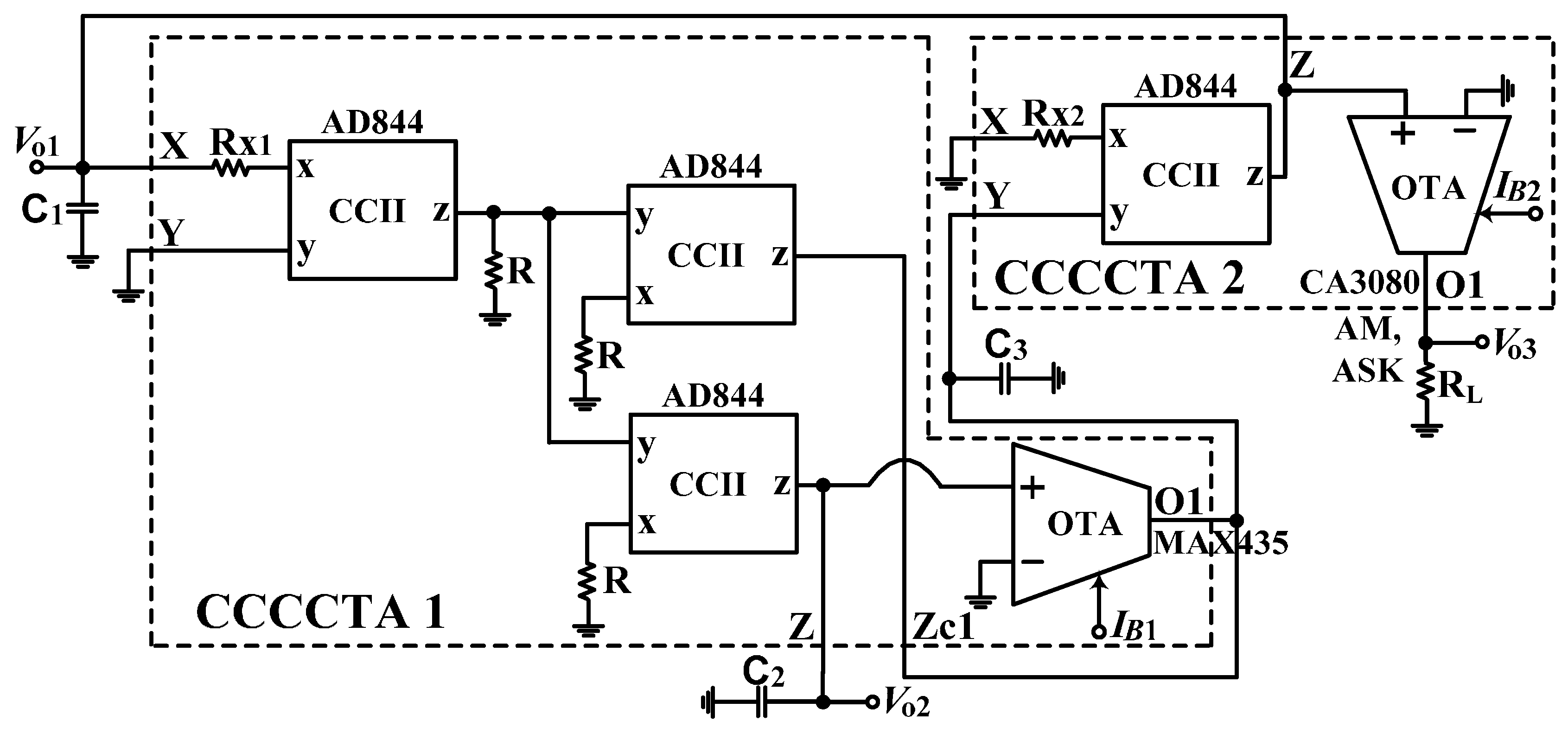
The MO-CCCCTA is not an off-the-shelf component but can be built by commercially available integrated circuits (ICs). For testing the proposed oscillator,
Figure 12 shows an equivalent method similar to
Figure 3 by using ready-to-use ICs, which include the operational amplifiers of AD844s and the operational transconductance amplifiers of MAX435 and CA3080. The DC power supply voltages are ±5 V. The
gm-value of the MAX435 is equal to 4/
Rg, where
Rg is an external resistor [
36]. In general, the applicability of such current-feedback operational amplifier (CFOA)-based oscillators is usually limited to a few hundred kilohertz [
37,
38].
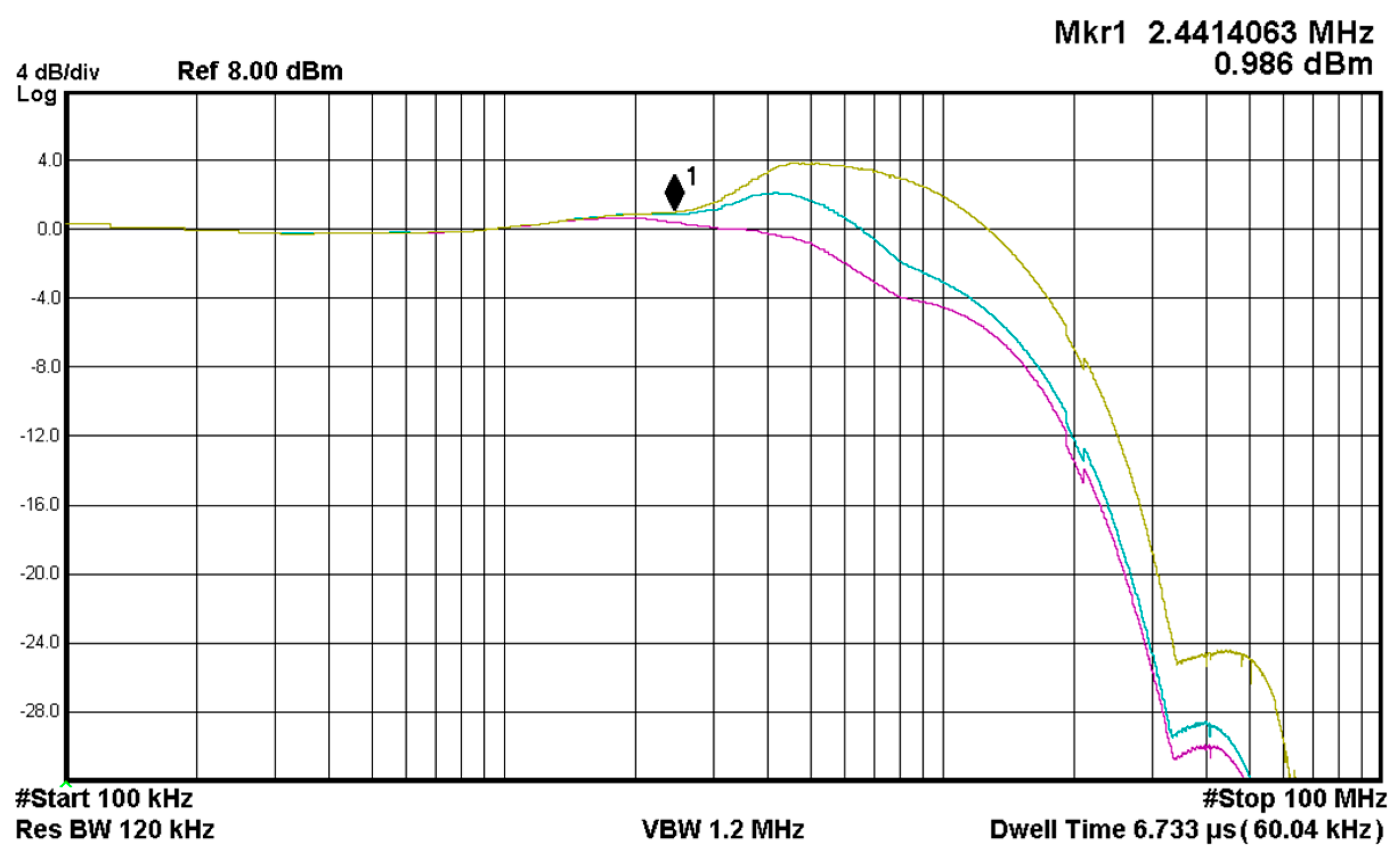
Figure 13 shows the experimental result of the frequency range of a commercially available AD844 with ±5 V DC supply. In
Figure 13, the values of the resistors were chosen as
R1 =
R2 = 1 kΩ (5 kΩ, 10 kΩ),
RL = 500 Ω,
CL = 10 pF, and the input power was 0 dBm.
Figure 14 is the measured result of a spectrum analyzer, which shows that the measured result of the frequency range of AD844 was limited to 2 MHz. The passive component values of the circuit in
Figure 12 were set as
gm1 = 1.428 mS (i.e.,
Rg = 2.8 kΩ),
RX1 = 0.73 kΩ,
RX2 = 0.7 kΩ,
R = 1 kΩ and
C1 =
C2 =
C3 = 750 pF, where
RX1 was designed to be larger than the theoretical value to ensure that the oscillator will start, before the centre frequency was obtained as
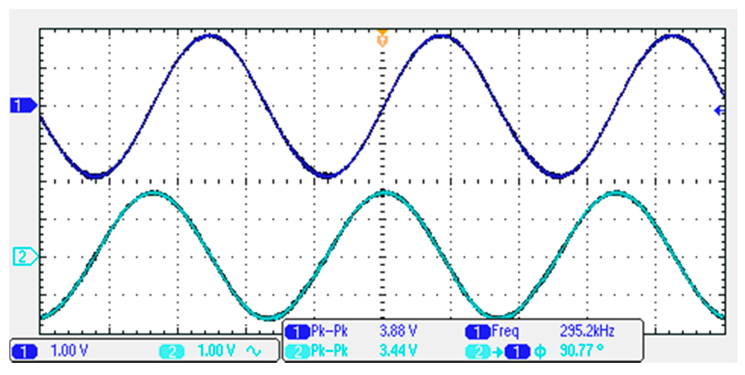
fo = 303.15 kHz. The oscilloscope output waveforms,
Vo1 and
Vo2, of the proposed oscillator are shown in
Figure 15, and the
X–
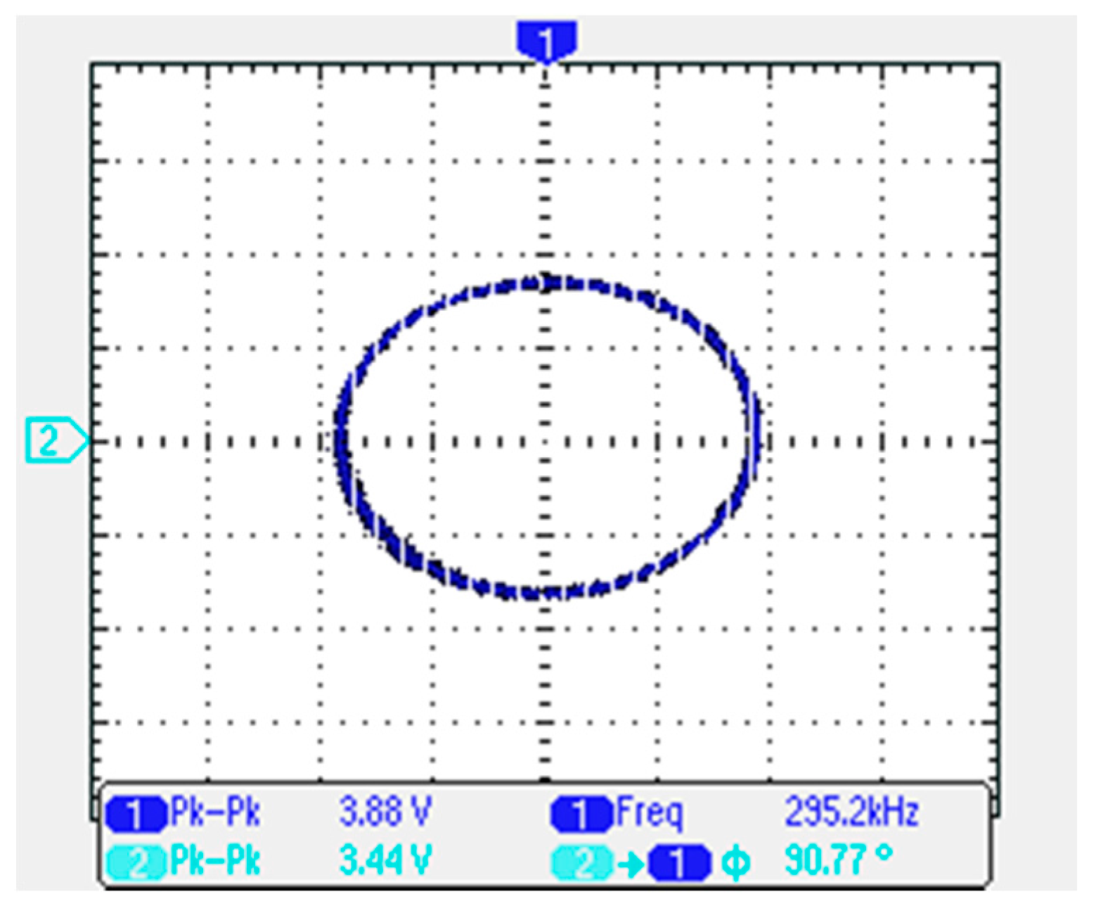
Y plot of
Vo1 and
Vo2 output voltages are shown in
Figure 16. The experimental oscillation frequency in
Figure 15 is 295.2 kHz, which is close to the theoretical value of 303.15 kHz with a 2.62% error rate.
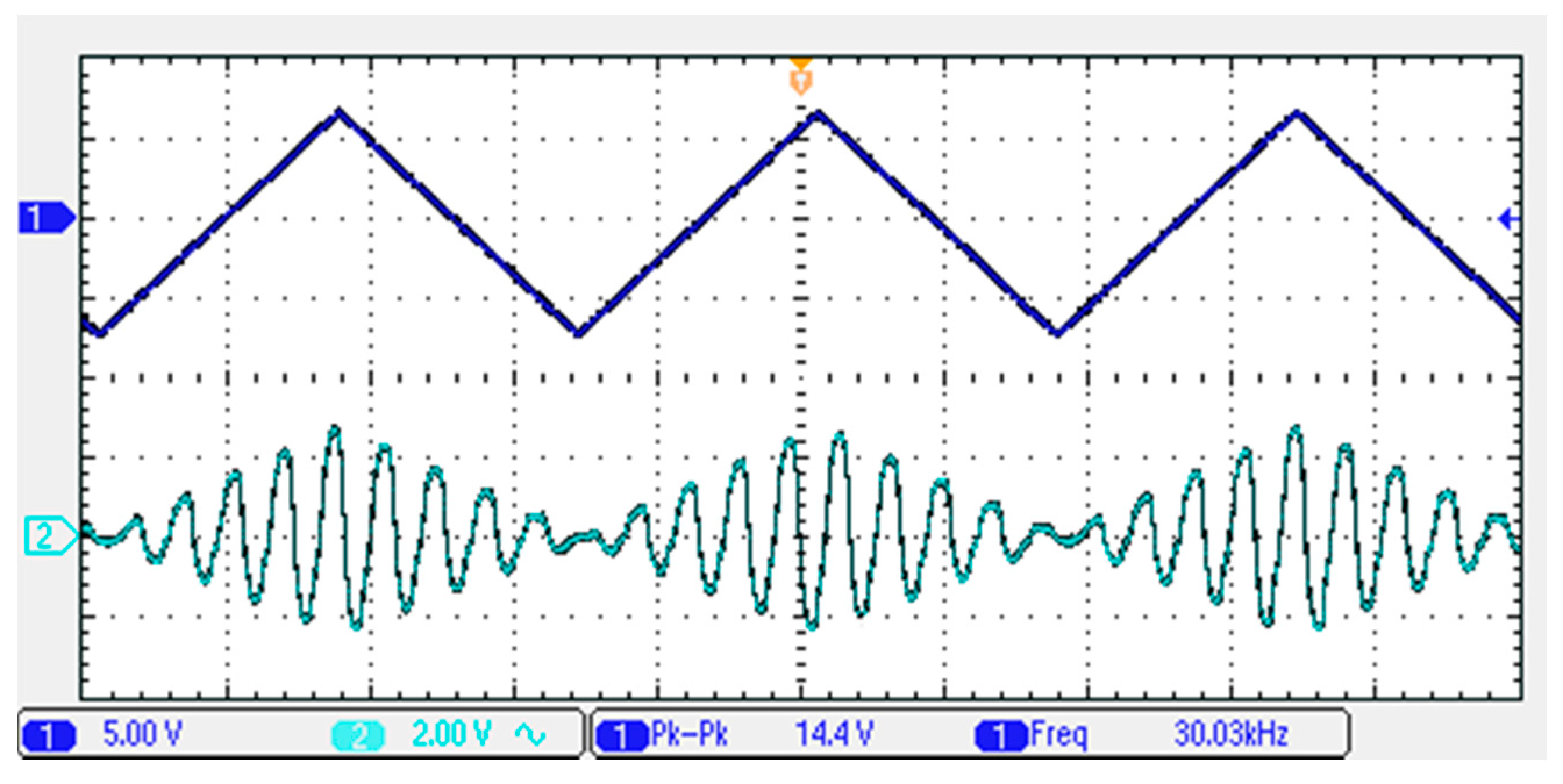
Figure 17,
Figure 18 and
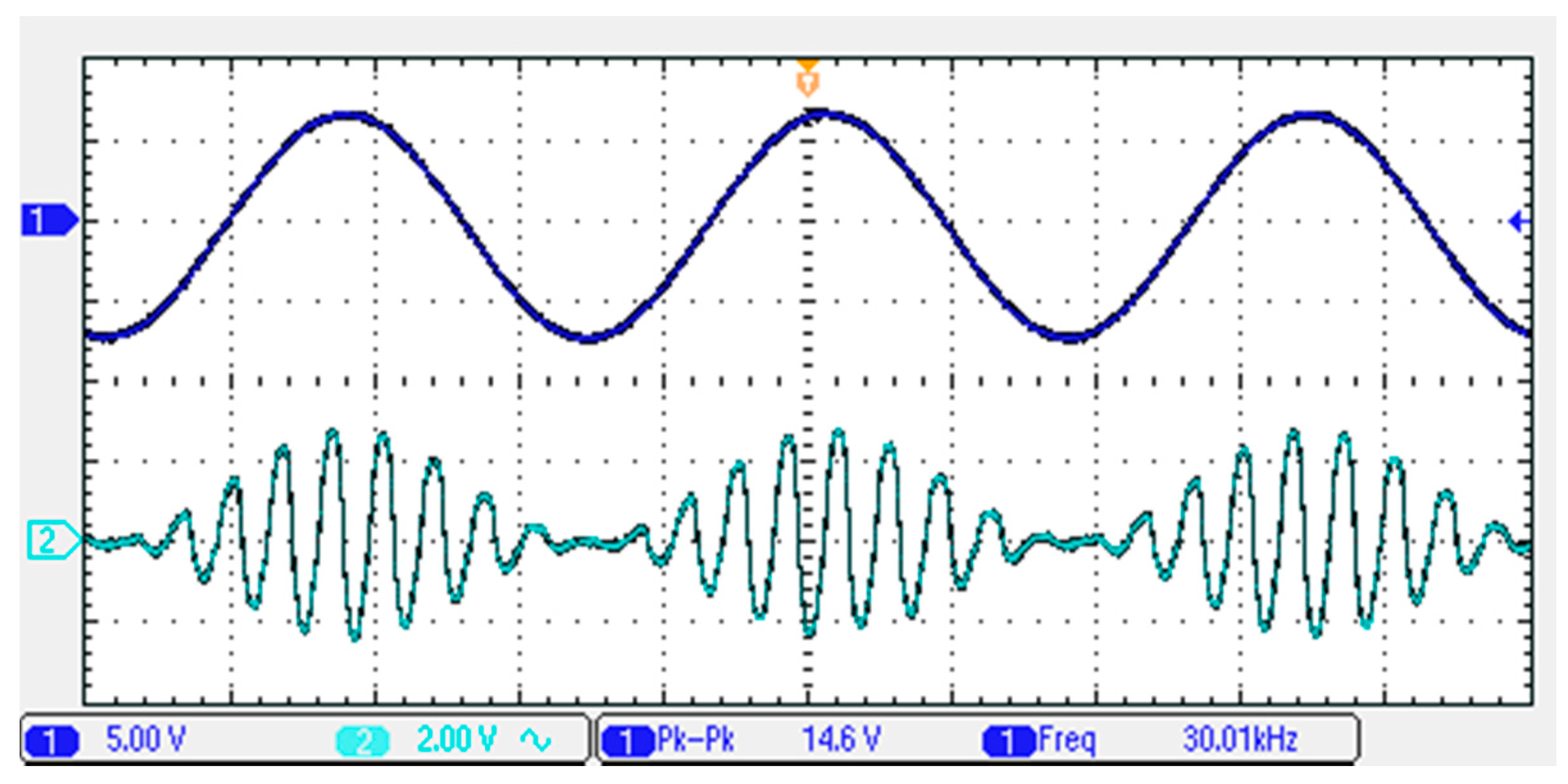
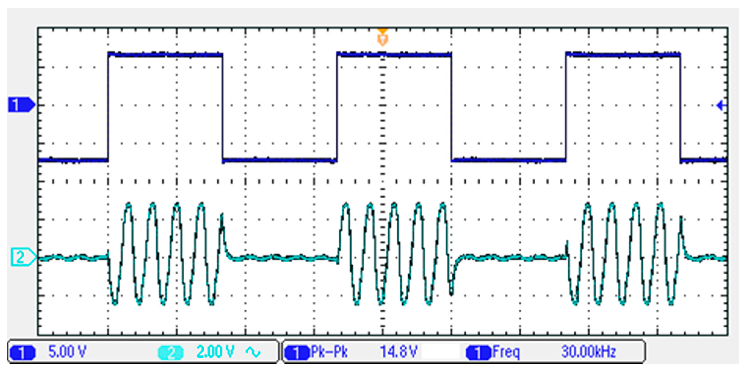
Figure 19 show the AM and the ASK signal outputs of the quadrature oscillator, where the modulation signal,
IB2, applied a sinusoidal signal, a triangular signal, or a pulse signal with a 30-kHz frequency. The experimental results are close to the theoretical analysis of Equation (12).
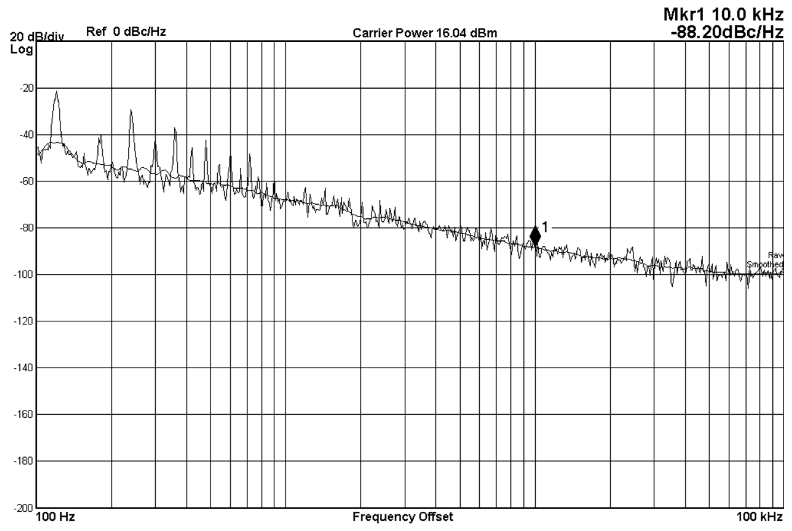
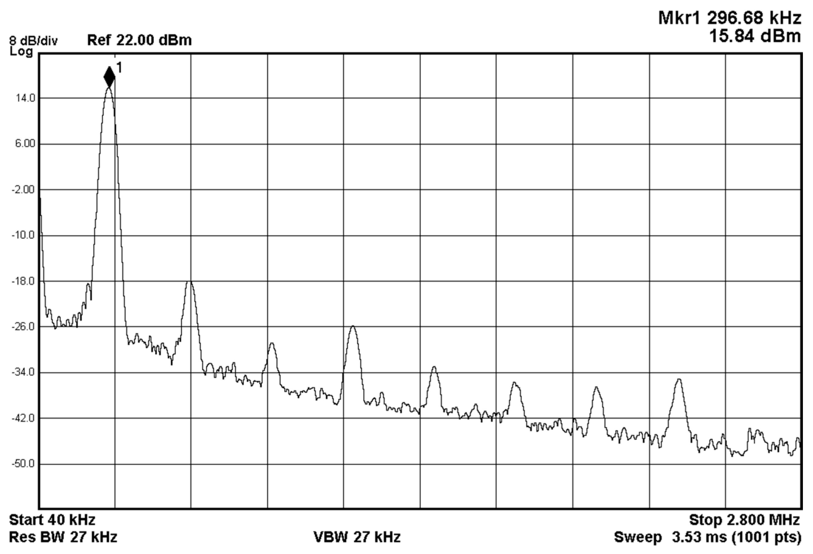
The frequency spectrum of the oscillator output voltage,
Vo1, is shown in
Figure 20. The measured oscillation frequency was 296.68 kHz, which is close to the theoretical value of 303.15 kHz with a 2.13% error rate. The THD, including the first harmonic through to the ninth harmonic components, is approximately 2.35%. The experimental results are consistent with the theoretical values. For oscillators, noise is a major concern where even a small noise in an oscillator will cause dramatic changes in its frequency spectrum and timing properties.
Figure 21 shows the phase noise using the Agilent phase noise measurement solution. The phase noise of the proposed oscillator is less than −88.2 dBc/Hz at 10 kHz offset.
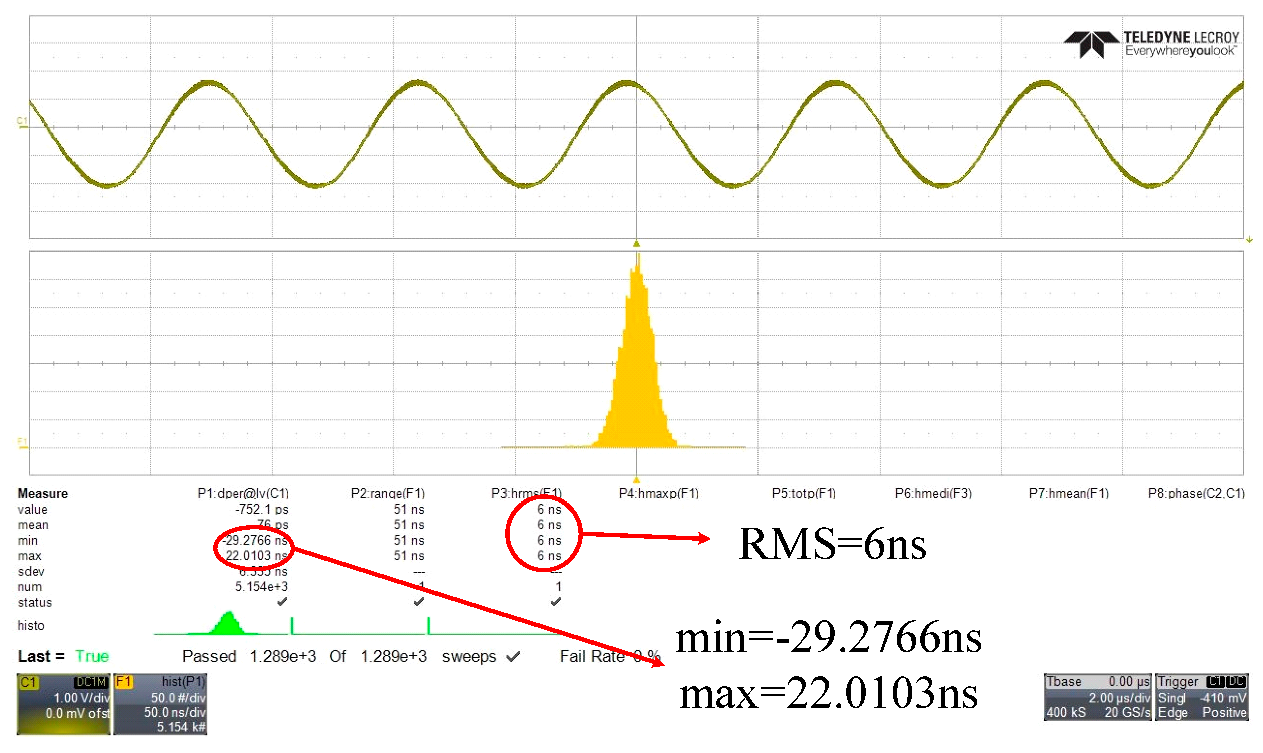
Figure 22 shows the root mean square (RMS) jitter of the proposed oscillator, which is 6 ns at an operating frequency of 295.2 kHz.


