Article

Thickness Dependence of Switching Behavior in Ferroelectric BiFeO3 Thin Films: A Phase-Field Simulation

Department of Physics, University of Science and Technology Beijing, Beijing 100083, China
*
Author to whom correspondence should be addressed.
Appl. Sci. 2017, 7(11), 1162; https://doi.org/10.3390/app7111162
Submission received: 26 September 2017 / Revised: 23 October 2017 / Accepted: 6 November 2017 / Published: 13 November 2017
(This article belongs to the Section Materials Science and Engineering)

Abstract

:
A phase-field approach to the analysis of the thickness effects in electric-field-induced domain switching in BiFeO3 thin films has been formulated. Time evolutions of domain switching percentage for films with different thicknesses were explored to reveal the primary switching path and its dependence on film thickness. In addition, hysteresis loop for these films were calculated to obtain their coercive fields. Results show a nonlinear thickness dependence of coercive field for ultrathin films. A parametric study of the interactions between film thickness, coercive field, current-voltage (I-V) response, and polarization switching behavior is herein discussed, which could provide physical insights into materials engineering.

1. Introduction

Nowadays, progresses in materials science and engineering have shown increasing reliance on the advantages of materials properties that originate from multi-field couplings. In ferroelectric materials, these properties include electrical-mechanical coupling (i.e., piezoelectricity [1,2] and flexoelectricity [3,4,5]), electrical-thermal coupling (i.e., pyroelectricity [6]), magneto-electricity [7] coupling, dielectricity [8,9], and so forth. All of the above properties involve the dynamics of ferroelectric polarization as well as reactions to externally applied fields. Electric-field-induced polarization switching in ferroelectric materials has attracted extensive attention from experimental [10] and theoretical [11,12,13,14] perspectives, owing to their unique features which can potentially provide improvements in data storage [15,16], spintronics [17], tunnel junctions [18], and non-volatile magnetoelectric devices [19]. As less voltage would be needed to generate the same electric field in thin films than that in thick ones, the basic understanding of underlying physics for thickness effects in switching behaviors is of great importance to the applications of ferroelectric thin films in miniaturized devices.
One of the most studied ferroelectric materials, BiFeO3 (BFO), simultaneously possesses ferroelectric properties and antiferromagnetic properties at room temperature, with Neel temperature T N ~ 643   K and Curie temperature T C ~ 1103   K [20,21,22,23]. The crystal structure of BFO below T C is a rhombohedrally distorted perovskite structure with its space group being R 3 c , [20] resulting in eight possible variants for spontaneous polarization in BFO, which can be denoted as R 1 ± = ± [ 111 ] ,   R 2 ± = ± [ 1 ¯ 11 ] ,   R 3 ± = ± [ 1 ¯ 1 ¯ 1 ] ,   R 4 ± = ± [ 1 1 ¯ 1 ] . Polarization switching arises when an external electric field is applied to the film. Due to the specialty of rhombohedral structures, only three paths are symmetrically allowed for polarization switching. According to the rotation angle, these switching paths can be defined as 71 degree switching, 109 degree switching, and 180 degree switching, respectively.
To discover the optimal conditions for BFO films in applications, Singh et al. successively studied the effect of film thickness, annealing treatments, processing temperatures, deposition substrates, and doping on the electric properties, particularly the polarization and leakage current density, of BFO thin films [24,25,26,27]. Lee et al. studied ferroelectric properties including polarization-electric-field (P-E) loop and leakage behavior for BFO films varying from 85 to 280 nm [28]. It was found that the coercive field decreased with increasing thickness. Similar conclusions were drawn by Tang et al. in a study about thickness-dependent multiferroic properties of BFO thin films, with film thicknesses ranging from 210 to 830 nm [29]. Theoretically, a thermodynamic model based on the Landau–Devonshire free energy expression and the Landau–Khalatnikov dynamic equation was employed to analyze the effects of film thickness and surface parameter on switching time and coercive field [30]. Results showed that the sign of surface parameter would determine the trend of coercive field changing with film thickness. Dead-layer effects in polarization switching has also been studied in ultrathin BFO films using both experimental methods and statistical analysis [31]. Chen and Lynch [12] proposed a micromechanics model to study polarization switching in tetragonal and rhombohedral structures and found that it is easier to move 90° (for tetragonal) and 70.5° (for rhombohedral) domain walls than 180° domain walls.
In our previous work [14], we studied the process of electric-field-induced polarization switching with a phase-field model, and the results show that 71 degree switching is the primary switching path when BFO films are subjected to electric fields. To fundamentally understand the effect of film thickness on polarization switching in BFO thin films, we employed a phase field model to simulate the switching behavior in films with various thicknesses. Further, corresponding hysteresis loops (P-E loops) and voltage-dependent leakage current (I-V responses) were also calculated, revealing the relationship between film thickness and coercive field.

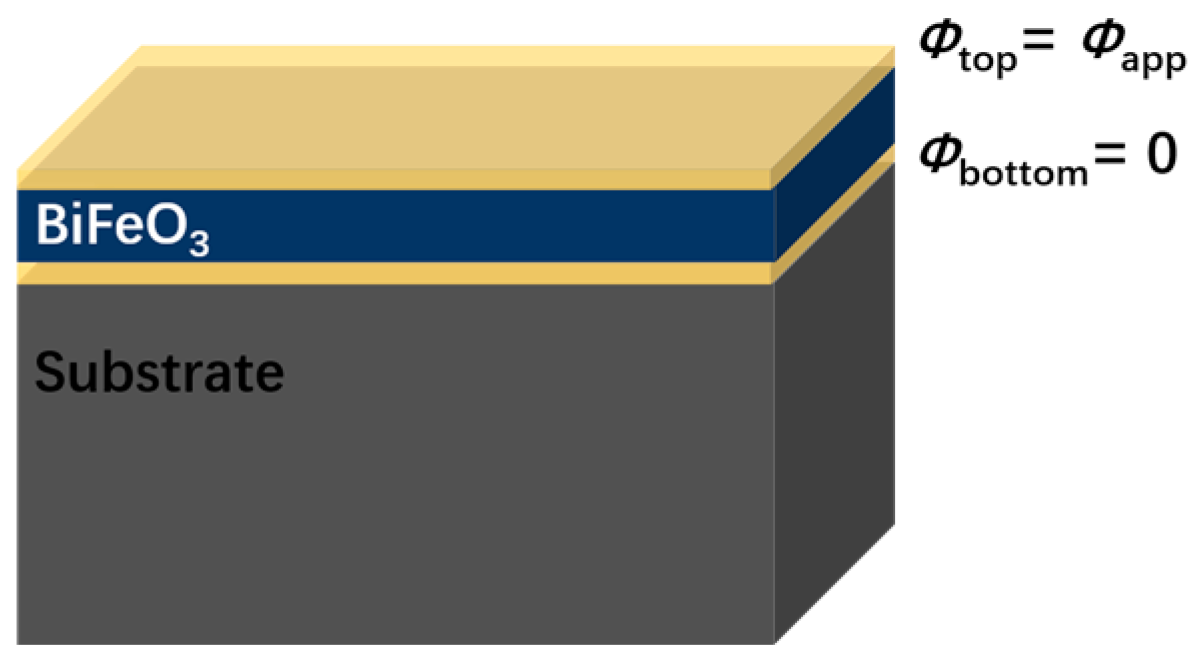
2. The Phase-Field Model

The present phase-field model describes ferroelectric domain configuration and evolution by polarization distributions P = ( P 1 , P 2 , P 3 ) . According to the Landau–Ginzburg–Devonshire theory, total free energy density for a ferroelectric single crystal is given by [14,32,33]
F = F Landau + F grad + F elas + F elec
in which F Landau ,   F grad ,   F elas ,   F elec represent Landau energy, gradient energy, elastic energy, and electrostatic energy, respectively.
Landau energy is expanded as a 4th order polynomial of the polarization components P i ( i = 1 ,   2 ,   3 ) :
F Landau = α 1 ( P 1 2 + P 2 2 + P 3 2 ) + α 11 ( P 1 4 + P 2 4 + P 3 4 ) + α 12 ( P 1 2 P 2 2 + P 1 2 P 3 2 + P 2 2 P 3 2 )
in which α 1 , α 11 , α 12 are Landau coefficients, and only α 1 is assumed to be temperature-dependent. Gradient energy, which represents the energy arising from the polarization gradient across domain walls, here is written as
F grad = 1 2 G 11 ( P i x j ) 2 ,   ( i , j = 1 , 2 , 3 )
in which G 11 is gradient energy coefficient, and x i is the ith component of the Cartesian coordinate system. Elastic energy, which is related to elastic strains originating from phase transitions or lattice accommodations, is written as
F elas = 1 2 c i j k l e i j e k l
in which c i j k l is the elastic stiffness tensor. e i j = ε i j ε i j 0 is the elastic strain, where ε i j is total strain, and ε i j 0 is stress-free strain, induced by spontaneous polarization via the electrostrictive effect:
ε i j 0 = Q i j k l P k P l ,   ( i , j , k , l = 1 , 2 , 3 )
where Q i j is the electrostrictive coefficient. Electrostatic energy is obtained from
F elec = ( E i P i + 1 2 ε b E i 2 )
in which E i is electric field, and ε b is the background dielectric constant.
Temporal evolution of the polarization distribution is governed by the time-dependent Ginzburg–Landau equation:
P i ( x , t ) t = L F P i ( x , t )
in which L is the kinetic coefficient related to the domain-wall mobility. In the model setting, we consider an epitaxial grown BFO film on a rigid substrate in the ( 001 ) c direction, as shown in Figure 1. Dimensions of the film are set as 128 Δ   ×   128 Δ   ×   h f Δ , in which h f is the grid number for the film thickness, and Δ is the grid size in the simulation. In the present work, Δ is set as 1 nm. A periodical boundary condition is applied along the x 1 and x 2 axes. A thin film mechanical boundary condition is adopted in this simulation [33]. As for the electric boundary condition of the film, a short circuit condition is applied in this model [34]. The top and bottom electrodes used in this model are shown in Figure 1. It is believed that electrode materials also have effects on the properties of films, because of their differences in chemical and thermal stabilities, especially the Schottky barrier height, which has an influence on leakage current [35,36,37]. However, in this work, with the purpose of generally studying the thickness effect in electric-field-induced multi-domain switching, we did not take the effect of electrodes as the primary concern of this study.
On the film-substrate surface, we have
ϕ | x 3 = 0 = 0
and on the top surface, we have
ϕ | x 3 = h f = ϕ app .
Electric field can be obtained through the following: E i = ϕ i ( i = 1 , 2 , 3 ) . The values of the coefficient for BFO in the simulation are as follows [14,32]: α 1 = 4.9 × ( T 1103 ) × 10 5   C 2 m 2 N , T = 298 K , α 11 = 6.5 × 10 8   C 4 m 6 N , α 12 = 1.0 × 10 8   C 4 m 6 N , c 11 = 302   GPa , c 12 = 162   GPa , c 44 = 68   GPa , Q 11 = 0.032   C 2 m 4 , Q 12 = 0.016   C 2 m 4 , and Q 44 = 0.02   C 2 m 4 .

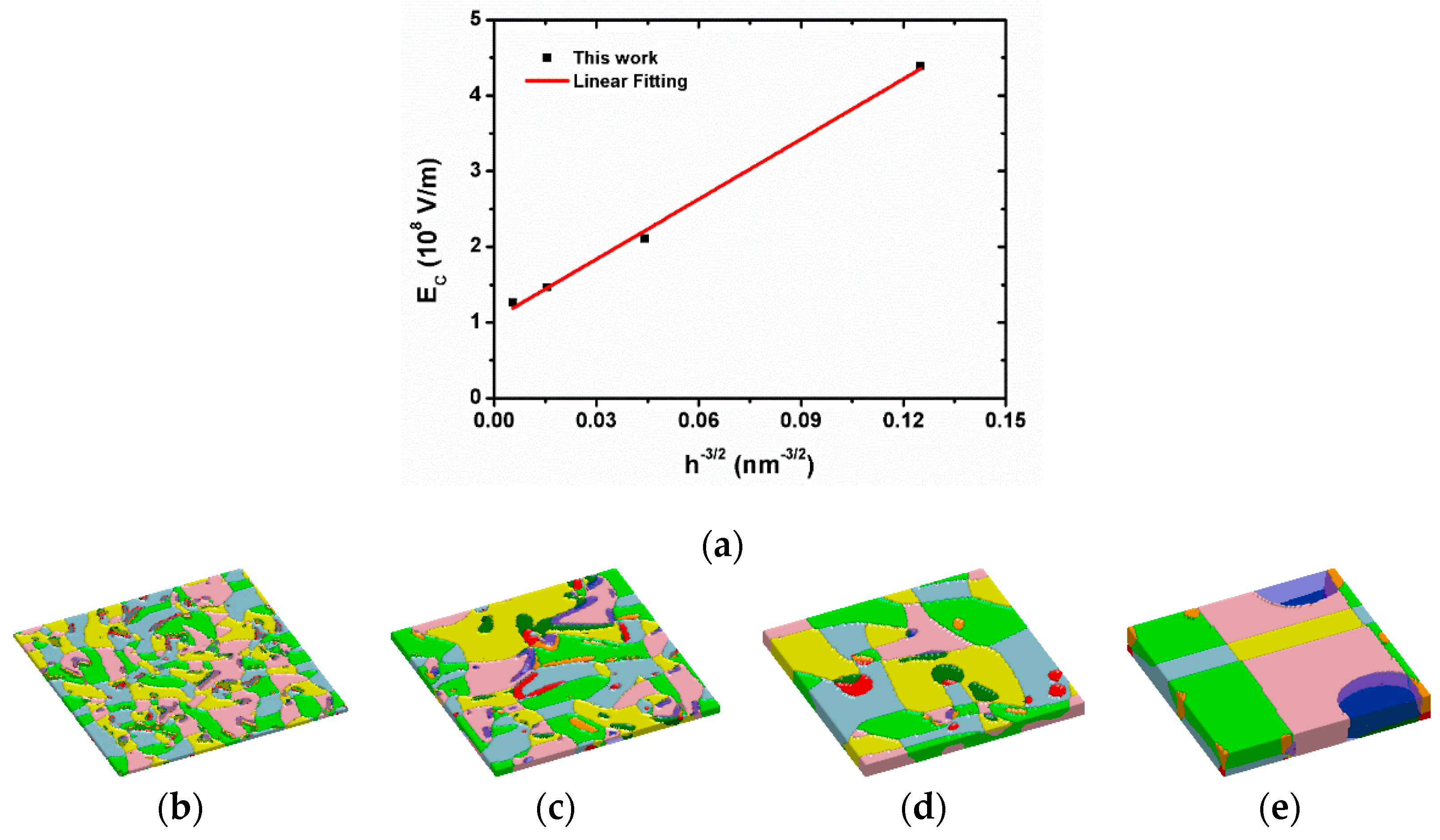
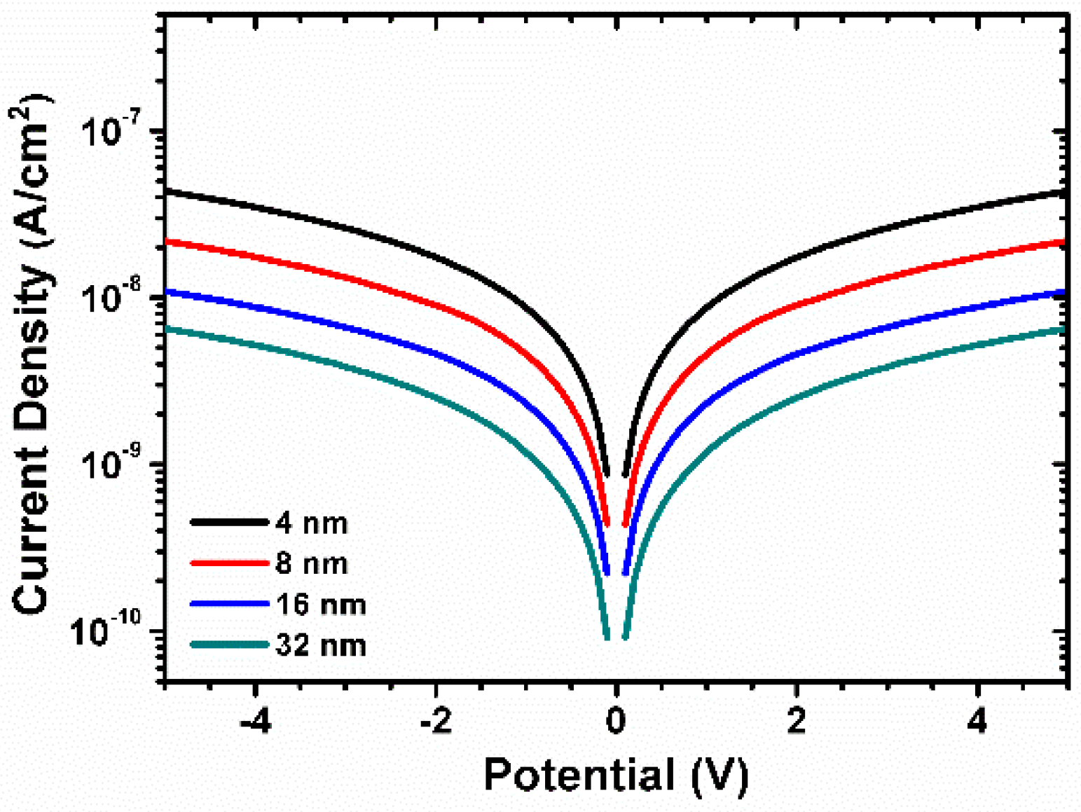
3. Results and Discussion

To study the effects of film thickness on the domain switching pathways in the BFO thin film, we performed three cases of different film thicknesses, where h = 32, 16 and 8 nm, using the above phase-field model. The BFO films are assumed to be epitaxial (001) oriented on a rigid substrate. Firstly, the system was evolved, without any external electric field, from a paraelectric phase to an energy minimizing domain configuration in a ferroelectric rhombohedral phase. Then, the electric field was uniformly applied as 500 kV/cm to the pre-evolved film in the direction perpendicular to the film surface for all three cases. The switching behavior was characterized by switching percentage, which was defined as the ratio of the number of grids that took switch action in a period of time via one specific switching path to the total grid number in the system. These percentages were calculated every 100 steps.
In all three cases, it was observed that domains switch to electric-field-favorable orientations mainly through a 71 degree switching path and that 180 degree switching is barely observed due to the relatively high energy bias, as also reported in our previous work [14]. Figure 2a presents the typical time evolutions of the switching percentage for three paths in the 32 nm BFO film. It could be seen that, in the switching process, 180 degree switching, which consumed the most energy, remained at zero, and the percentage of the 109 degree switching path was even lower than 1%. The 71 degree path was the dominant one for polarization switching in the rhombohedral BFO films. To study the effect of thickness, switching percentages for this primary switching path in films with different thicknesses were compared (Figure 2b). For all samples, with an application of the constant electric field, polarization switching percentages burst into a maximum value in the beginning and drop to zero as time goes on. Films with different thickness have different decreasing tendencies, indicating different switching times.
Here, we plotted the detailed volume fractions for upward variants R+ ( R 1 + ,   R 2 + ,   R 3 + ,   R 4 + ) and downward variants R- ( R 1 ,   R 2 ,   R 3 ,   R 4 ) in these samples in Figure 3. As the system evolved under an applied downward electric field, energy-unfavorable variants (in this case, the upward variants R+) disappeared over time. We used the vanishing point of R+ as the end of electric-field-induced polarization switching. In the 32 nm film, the volume fraction of R+ dropped to zero around Step 1000. In the 16 nm film, this drop occurred at Step 3000, and, in the 8 nm film, at Step 7000. With the decrease of film thicknesses, the time that was needed for the system to finish the switching process became longer.
The difference in the performance of domain switching between films with distinct thicknesses can be attributed to the influence of the coercive field. To study the relationship between film thickness and coercive field, ferroelectric hysteresis loops for films with different thicknesses— h = 32 ,   16 ,   8 ,   4   nm —were calculated. Selected corresponding domain configurations were presented as well.
Hysteresis loops were calculated by applying dynamic electric potentials on top of the film, following the order 0   V 5   V 5   V 5   V . Consequently, electric fields were generated in directions downward/upward perpendicular to the film surface. Applying positive potentials on top of the film would result in a downward electric field, which further gave rise to downward polarizations (represented with negative signs in Figure 4). On the contrary, negative potentials led to the expansion of upward variants at the expense of downward ones. Domain configurations close to saturation polarizations (Points A and C) and coercive fields (Points B and D) were shown alongside the P-E loops. At Saturation Point A, domains were mainly formed by the four downward variants: R 1 ,   R 2 ,   R 3 ,   R 4 . As the period of electric field gradually decreased from positive maximum to zero, polarization dropped slowly, suggesting high remnant polarization, especially in thick films. When the reverse electric field grew, particularly near the coercive field (Point B), opposite variants started to emerge around the domain walls, and their areas expanded over domains with the strengthening of electric potential, which was the result of the electric-field-induced polarization switching. As opposite polarizations reached a maximum (Point C), domains were mainly formed by the four upward variants: R 1 + ,   R 2 + ,   R 3 + ,   R 4 + . In the process of a gradually changing electric potential from −5 V (Point C) to 5 V (Point A), polarizations in films switched from upward to downward via the turning Point D. As film thickness decreased from 32 nm in Figure 4a to 4 nm in Figure 4d, domain width decreased remarkably, which is a size effect—also reported in the literature [38,39].
Another important effect of the thickness is the changed coercive field. In Figure 4, it is clear that the coercive potential, at which total polarizations become zero, decreases as film thickness decreases. In order to obtain the critical effect of thickness, coercive field is derived by dividing the coercive potential by the film thickness, as follows: E c = U c h , in which E c is the coercive field, U c is coercive potential obtained from the P-E loop, and h is the corresponding film thickness.
From Figure 5, the relation between coercive fields and film thicknesses can generally be expressed as E c h 3 2 , which has a similar trend as the well-known Kay-Dunn law ( E c h 2 3 ) [40], but a greater value in power. This is because the Kay–Dunn law was derived from films with millimeter scale thickness, in which a switching process originated from nucleation. Yet in our work, the systems we studied are ultrathin films, and the polarization switching mechanism can be quite different due to the size effect [31,41]. We can see from the calculated domain configurations in Figure 5 that the domain width of the 4 nm film is much smaller than the width of the 32 nm film, which means that there are more domain boundaries in the 4 nm film. As seen in the figure, domain boundaries would block the process of domain switching, so thinner film will have a higher coercive field. The results that the coercive field decreases with increasing film thickness, and that thicker films have faster switching processes, confirm the general relation between switching time and coercive field [42]: t s 1 E E c , where t s is switching time, E is applied electric field, and E c is corresponding coercive field.
Additionally, I-V response is also an important character for ferroelectric films when they are subject to electric potentials. Therefore, we further studied the leakage current evolution under varying applied potentials [43]. The calculated I-V response for films with different thicknesses are shown in Figure 6. The leakage current density in BFO films increases markedly in samples with small thicknesses, indicating the limitations of application for ultrathin films.

4. Conclusions

The effects of film thickness on polarization switching paths were investigated using phase-field modeling. Results indicate that 71 degree switching plays the most important role in the polarization switching process. Analysis of time-dependent switching percentages in different films shows that polarization switching time increases as film thickness decreases. Calculations of the hysteresis loop for films with different film thicknesses reveal the dependence of a ferroelectric coercive field on film thickness, as E c h 3 2 , in ultrathin BFO films, which could potentially provide guidance in future theoretical research and material design and discovery.

Acknowledgments

This work is supported by the National Science Foundation of China (No. 11504020 and No. 11174030) and the Fundamental Research Funds for the Central Universities (FRF-TP-16-064A1).

Author Contributions

Xingqiao Ma and Guoping Cao conceived and designed the simulation; Guoping Cao performed the calculation; Houbing Huang and Guoping Cao analyzed the data; Guoping Cao wrote the paper.

Conflicts of Interest

The authors declare no conflict of interest.

References

  1. Li, F.; Zhang, S.; Yang, T.; Xu, Z.; Zhang, N.; Liu, G.; Wang, J.; Wang, J.; Cheng, Z.; Ye, Z.-G. The origin of ultrahigh piezoelectricity in relaxor-ferroelectric solid solution crystals. Nat. Commun. 2016, 7, 13807. [Google Scholar] [CrossRef] [PubMed]
  2. Reed, E.J. Piezoelectricity: Now in two dimensions. Nat. Nanotechnol. 2015, 10, 106–107. [Google Scholar] [CrossRef] [PubMed]
  3. Tagantsev, A.K.; Yudin, P.V. Flexoelectricity in Solids: From Theory to Applications; World Scientific: Singapore, 2016. [Google Scholar]
  4. Gu, Y.; Li, M.; Morozovska, A.N.; Wang, Y.; Eliseev, E.A.; Gopalan, V.; Chen, L.-Q. Flexoelectricity and ferroelectric domain wall structures: Phase-field modeling and dft calculations. Phys. Rev. B 2014, 89, 174111. [Google Scholar] [CrossRef]
  5. Jiang, L.; Zhou, Y.; Zhang, Y.; Yang, Q.; Gu, Y.; Chen, L.-Q. Polarization switching of the incommensurate phases induced by flexoelectric coupling in ferroelectric thin films. Acta Mater. 2015, 90, 344–354. [Google Scholar] [CrossRef]
  6. Scott, J. Contribution to pyroelectricity from domain walls and substrate strain. Ferroelectrics 2014, 472, 19–28. [Google Scholar] [CrossRef]
  7. Hu, J.M.; Chen, L.Q.; Nan, C.W. Multiferroic heterostructures integrating ferroelectric and magnetic materials. Adv. Mater. 2016, 28, 15–39. [Google Scholar] [CrossRef] [PubMed]
  8. Jahani, S.; Jacob, Z. All-dielectric metamaterials. Nat. Nanotechnol. 2016, 11, 23–36. [Google Scholar] [CrossRef] [PubMed]
  9. Cao, G.; Huang, H.; Liang, D.; Ma, X. A phenomenological potential and ferroelectric properties of BaTiO3–CaTiO3 solid solution. Ceram. Int. 2017, 43, 6671–6676. [Google Scholar] [CrossRef]
  10. Li, J.; Nagaraj, B.; Liang, H.; Cao, W.; Lee, C.H.; Ramesh, R. Ultrafast polarization switching in thin-film ferroelectrics. Appl. Phys. Lett. 2004, 84, 1174–1176. [Google Scholar] [CrossRef]
  11. Hwang, S.; Lynch, C.; McMeeking, R. Ferroelectric/ferroelastic interactions and a polarization switching model. Acta Metall. Mater. 1995, 43, 2073–2084. [Google Scholar] [CrossRef]
  12. Chen, W.; Lynch, C. A micro-electro-mechanical model for polarization switching of ferroelectric materials. Acta Mater. 1998, 46, 5303–5311. [Google Scholar] [CrossRef]
  13. Wang, J.; Shi, S.-Q.; Chen, L.-Q.; Li, Y.; Zhang, T.-Y. Phase-field simulations of ferroelectric/ferroelastic polarization switching. Acta Mater. 2004, 52, 749–764. [Google Scholar] [CrossRef]
  14. Cao, G.; Cao, Y.; Huang, H.; Chen, L.-Q.; Ma, X. Analysis of multi-domain ferroelectric switching in BiFeO3 thin film using phase-field method. Comput. Mater. Sci. 2016, 115, 208–213. [Google Scholar] [CrossRef]
  15. Scott, J.F. Searching for new ferroelectrics and multiferroics: A user’s point of view. NPJ Comput. Mater. 2015, 1, 15006. [Google Scholar] [CrossRef] [Green Version]
  16. Catalan, G.; Scott, J.F. Physics and applications of bismuth ferrite. Adv. Mater. 2009, 21, 2463–2485. [Google Scholar] [CrossRef]
  17. Béa, H.; Gajek, M.; Bibes, M.; Barthélémy, A. Spintronics with multiferroics. J. Phys. Condens. Matter 2008, 20, 434221. [Google Scholar] [CrossRef]
  18. Gajek, M.; Bibes, M.; Fusil, S.; Bouzehouane, K.; Fontcuberta, J.; Barthélémy, A.; Fert, A. Tunnel junctions with multiferroic barriers. Nat. Mater. 2007, 6, 296–302. [Google Scholar] [CrossRef] [PubMed]
  19. Baek, S.; Jang, H.; Folkman, C.; Li, Y.; Winchester, B.; Zhang, J.; He, Q.; Chu, Y.; Nelson, C.; Rzchowski, M. Ferroelastic switching for nanoscale non-volatile magnetoelectric devices. Nat. Mater. 2010, 9, 309–314. [Google Scholar] [CrossRef] [PubMed]
  20. Michel, C.; Moreau, J.-M.; Achenbach, G.D.; Gerson, R.; James, W.J. The atomic structure of BiFeO3. Solid State Commun. 1969, 7, 701–704. [Google Scholar] [CrossRef]
  21. Kubel, F.; Schmid, H. Structure of a ferroelectric and ferroelastic monodomain crystal of the perovskite BiFeO3. Acta Crystallogr. Sect. B 1990, 46, 698–702. [Google Scholar] [CrossRef]
  22. Zavaliche, F.; Yang, S.; Zhao, T.; Chu, Y.; Cruz, M.; Eom, C.; Ramesh, R. Multiferroic BiFeO3 films: Domain structure and polarization dynamics. Phase Transit. 2006, 79, 991–1017. [Google Scholar] [CrossRef]
  23. Wu, J.; Fan, Z.; Xiao, D.; Zhu, J.; Wang, J. Multiferroic bismuth ferrite-based materials for multifunctional applications: Ceramic bulks, thin films and nanostructures. Prog. Mater. Sci. 2016, 84, 335–402. [Google Scholar] [CrossRef]
  24. Singh, S.K.; Ishiwara, H. Reduced leakage current in BiFeO3 thin films on Si substrates formed by a chemical solution method. Jpn. J. Appl. Phys. 2005, 44, L734. [Google Scholar] [CrossRef]
  25. Singh, S.K.; Ueno, R.; Funakubo, H.; Uchida, H.; Koda, S.; Ishiwara, H. Dependence of ferroelectric properties on thickness of BiFeO3 thin films fabricated by chemical solution deposition. Jpn. J. Appl. Phys. 2005, 44, 8525. [Google Scholar] [CrossRef]
  26. Singh, S.; Ishiwara, H.; Maruyama, K. Enhanced polarization and reduced leakage current in BiFeO3 thin films fabricated by chemical solution deposition. J. Appl. Phys. 2006, 100, 064102. [Google Scholar] [CrossRef]
  27. Rajput, S.; Katoch, R.; Sahoo, K.; Sharma, G.; Singh, S.; Gupta, R.; Garg, A. Enhanced electrical insulation and ferroelectricity in La and Ni co-doped BiFeO3 thin films. J. Alloys Compd. 2015, 621, 339–344. [Google Scholar] [CrossRef]
  28. Lee, C.-C.; Wu, J.-M. Effect of film thickness on interface and electric properties of BiFeO3 thin films. Appl. Surf. Sci. 2007, 253, 7069–7073. [Google Scholar] [CrossRef]
  29. Tang, X.; Dai, J.; Zhu, X.; Lin, J.; Chang, Q.; Wu, D.; Song, W.; Sun, Y. Thickness-dependent dielectric, ferroelectric, and magnetodielectric properties of BiFeO3 thin films derived by chemical solution deposition. J. Am. Ceram. Soc. 2012, 95, 538–544. [Google Scholar] [CrossRef]
  30. Musleh Alrub, A.; Ong, L.-H. Thickness dependence of switching time and coercive field in ferroelectric thin films. J. Appl. Phys. 2011, 109, 084109. [Google Scholar] [CrossRef]
  31. Maksymovych, P.; Huijben, M.; Pan, M.; Jesse, S.; Balke, N.; Chu, Y.-H.; Chang, H.J.; Borisevich, A.Y.; Baddorf, A.P.; Rijnders, G. Ultrathin limit and dead-layer effects in local polarization switching of BiFeO3. Phys. Rev. B 2012, 85, 014119. [Google Scholar] [CrossRef]
  32. Zhang, J.; Li, Y.; Choudhury, S.; Chen, L.; Chu, Y.; Zavaliche, F.; Cruz, M.; Ramesh, R.; Jia, Q. Computer simulation of ferroelectric domain structures in epitaxial BiFeO3 thin films. J. Appl. Phys. 2008, 103, 094111. [Google Scholar] [CrossRef]
  33. Chen, L.Q. Phase-field method of phase transitions/domain structures in ferroelectric thin films: A review. J. Am. Ceram. Soc. 2008, 91, 1835–1844. [Google Scholar] [CrossRef]
  34. Li, Y.; Hu, S.; Liu, Z.; Chen, L. Effect of electrical boundary conditions on ferroelectric domain structures in thin films. Appl. Phys. Lett. 2002, 81, 427–429. [Google Scholar] [CrossRef]
  35. Nagaraj, B.; Aggarwal, S.; Ramesh, R. Influence of contact electrodes on leakage characteristics in ferroelectric thin films. J. Appl. Phys. 2001, 90, 375–382. [Google Scholar] [CrossRef]
  36. Izyumskaya, N.; Alivov, Y.-I.; Cho, S.-J.; Morkoç, H.; Lee, H.; Kang, Y.-S. Processing, structure, properties, and applications of PZT thin films. Crit. Rev. Solid State Mater. Sci. 2007, 32, 111–202. [Google Scholar] [CrossRef]
  37. Tomczyk, M.; Stroppa, D.G.; Reaney, I.M.; Vilarinho, P.M. Growth of BiFeO3 thin films by chemical solution deposition: The role of electrodes. Phys. Chem. Chem. Phys. 2017, 19, 14337–14344. [Google Scholar] [CrossRef] [PubMed]
  38. Gotō, K. Thickness dependence of the domain width in thin crystals of BaFe12O19 and SrFe12O19. Jpn. J. Appl. Phys. 1966, 5, 117. [Google Scholar] [CrossRef]
  39. Huang, C.; Chen, L.; Wang, J.; He, Q.; Yang, S.; Chu, Y.; Ramesh, R. Phenomenological analysis of domain width in rhombohedral BiFeO3 films. Phys. Rev. B 2009, 80, 140101. [Google Scholar] [CrossRef]
  40. Kay, H.; Dunn, J. Thickness dependence of the nucleation field of triglycine sulphate. Philos. Mag. 1962, 7, 2027–2034. [Google Scholar] [CrossRef]
  41. Jo, J.; Kim, Y.; Noh, T.; Yoon, J.-G.; Song, T. Coercive fields in ultrathin BaTiO3 capacitors. Appl. Phys. Lett. 2006, 89, 232909. [Google Scholar] [CrossRef]
  42. Merz, W.J. Domain formation and domain wall motions in ferroelectric BaTiO3 single crystals. Phys. Rev. 1954, 95, 690. [Google Scholar] [CrossRef]
  43. Cao, Y.; Shen, J.; Randall, C.; Chen, L. Phase-field modeling of switchable diode-like current-voltage characteristics in ferroelectric BaTiO3. Appl. Phys. Lett. 2014, 104, 182905. [Google Scholar] [CrossRef]
Figure 1. Schematic illustration of the ferroelectric BiFeO3 (BFO) thin film model.
Applsci 07 01162 g001
Figure 2. Analysis of domain switching behavior for different film thicknesses using an identical electric field: E = 500   kV / cm . (a) Switching percentage of different switching paths as a function of time in the h = 32   nm film. (b) Percentage for 71 degree switching over time, with different film thicknesses indicated with different colors.
Applsci 07 01162 g002
Figure 3. Time evolution of volume fractions for downward (R- with solid line) and upward (R+ with dot line) variants. Films with different thicknesses (32, 16, and 8 nm) are indicated with different colors.
Applsci 07 01162 g003
Figure 4. Hysteresis loops (P-E loops) for thin films with different film thicknesses: (a) 32 nm, (b) 16 nm, (c) 8 nm, and (d) 4 nm. Domain patterns for specific points are provided alongside the P-E loop. (e) Representative colors for eight rhombohedral variants in domain patterns.
Applsci 07 01162 g004aApplsci 07 01162 g004b
Figure 5. (a) Calculated coercive field E c plotted against film thickness h . Calculated domain configurations near the value of coercive field for films of (b) 4 nm, (c) 8 nm, (d) 16 nm, and (e) 32 nm.
Applsci 07 01162 g005
Figure 6. Current-voltage (I-V) response of films with different thicknesses at room temperature.
Applsci 07 01162 g006

