Article

The Positive Effects of Hydrophobic Fluoropolymers on the Electrical Properties of MoS2 Transistors

1
Department of Electrical and Computer Engineering, University of Texas at Austin, Austin, TX 78758, USA
2
Microelectronics Research Center, University of Texas at Austin, Austin, TX 78758, USA
*
Author to whom correspondence should be addressed.
Appl. Sci. 2016, 6(9), 236; https://doi.org/10.3390/app6090236
Submission received: 19 July 2016 / Revised: 11 August 2016 / Accepted: 12 August 2016 / Published: 23 August 2016
(This article belongs to the Special Issue Two-Dimensional Transition Metal Dichalcogenides)

Abstract

:
We report the improvement of the electrical performance of field effect transistors (FETs) fabricated on monolayer chemical vapor deposited (CVD) MoS2, by applying an interacting fluoropolymer capping layer (Teflon-AF). The electrical characterizations of more than 60 FETs, after applying Teflon-AF cap, show significant improvement of the device properties and reduced device to device variation. The improvement includes: 50% reduction of the average gate hysteresis, 30% reduction of the subthreshold swing and about an order of magnitude increase of the current on-off ratio. These favorable changes in device performance are attributed to the reduced exposure of MoS2 channels to the adsorbates in the ambient which can be explained by the polar nature of Teflon-AF cap. A positive shift in the threshold voltage of all the measured FETs is observed, which translates to the more desirable enhancement mode transistor characteristics.

Graphical Abstract

1. Introduction

Two dimensional atomic solids such as graphene and transition metal dichalcogenides (TMDs) have attracted a great amount of interest due to their thickness-dependent electrical and optical properties. Of TMDs, Molybdenum disulfide, (MoS2), with its indirect to direct band gap transition as a function of layer thickness has been of particular interest for digital and optoelectronic applications [1,2,3,4]. MoS2 has already been used to fabricate functional electronic circuit elements [5,6], as well as opto-electronic devices [7], and coupled electro-mechanic systems [8,9]. Recent research has also shown its applicability for high frequency applications [10,11]. Also, the recent progress towards the wafer-scale growth and batch fabrication of field-effect transistors (FETs) on chemical vapor deposited (CVD) monolayer 2D solids such as graphene [12] and recently MoS2 and WS2 [13], has shown great promise for realizing commercial applications of these materials.
However, the performance of FETs fabricated on these wafer-scale films are largely impacted by device to device variability, including gate hysteresis and threshold voltage variations, e.g. threshold voltage of ~100 tested MoS2 FETs, fabricated on 100-mm silicon substrates, ranges between 10 V and 45 V with the reported mobility in 1–40 cm2/Vs range and high variability in the current on-off ratio and gate hysteresis. This significant performance variability are often caused by the charges trapped between the 2D device channel and the gate dielectric as well as oxygen and moisture chemisorption at the basal plane and edges of MoS2 [14,15,16,17]. Therefore, one way to reduce performance variability and gate hysteresis is taking the measurements under vacuum or long-term annealing of MoS2 FETs at elevated temperatures prior to testing the device [18]. Both of these techniques leads to removing the adsorbed oxygen/moisture content from the MoS2 channel surface. A second method to reduce the channel interaction with the ambient, is to apply hydrophobic capping layers to the top surface of the device. Previous reports have shown that the performance variations of graphene and carbon nanotube (CNT) FETs can be reduced by applying a monolayer self-assembled hexamethyldisilazane (HMDS) layer between the back gate dielectric and the device channel or on the top surface of the device channels [18,19,20]. Other reports showed that passivating the surface of graphene and phosphorene FETs by a thicker hydrophobic film, such as fluoropolymers, results in more lasting positive changes and improved consistency in device to device performance [21,22,23].
Here, we report the impact of encapsulation of MoS2 FETs by a hydrophobic fluoropolymer, Teflon-AF. Our results show significant improvement in key device performance metrics such as current on-off ratio, subthreshold swing and gate hysteresis. Key performance metrics, such as threshold voltage, subthreshold swing, gate hysteresis and on-off ratio also show improved consistency after applying the fluoropolymer cap.

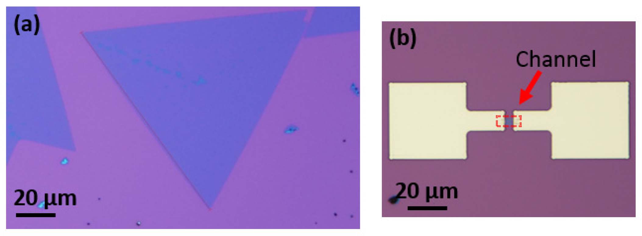
2. Materials and Methods
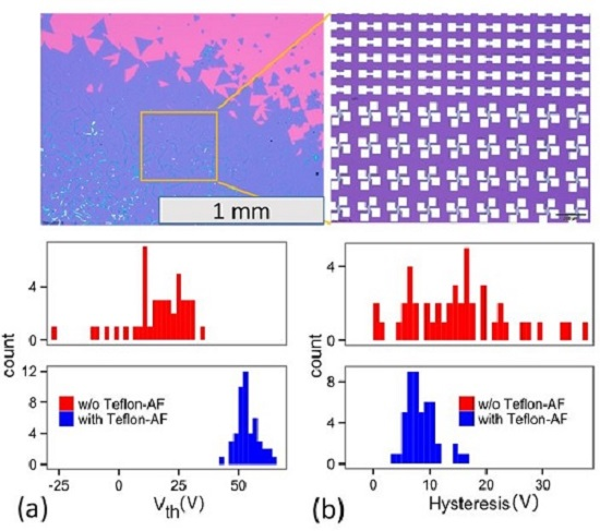
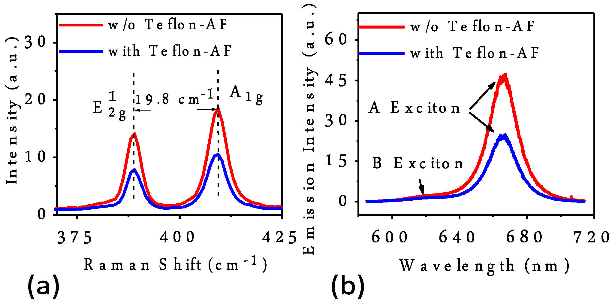
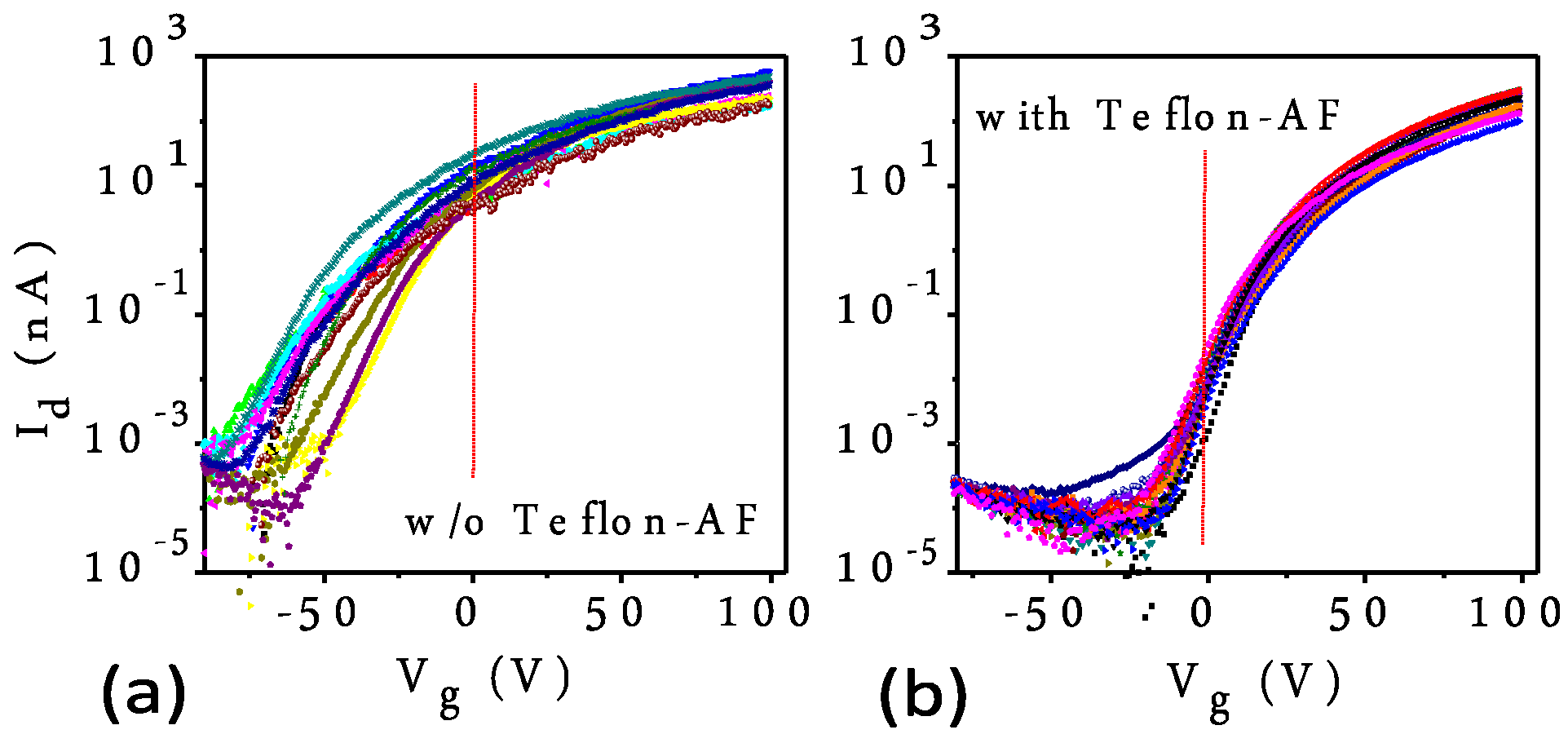
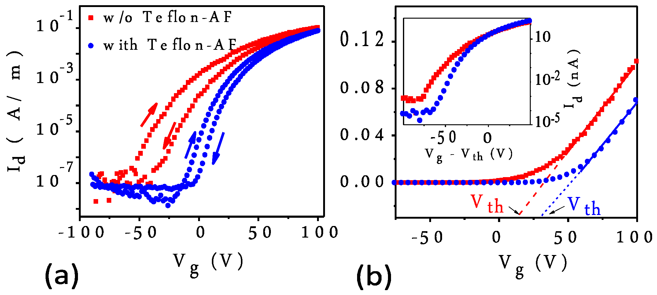
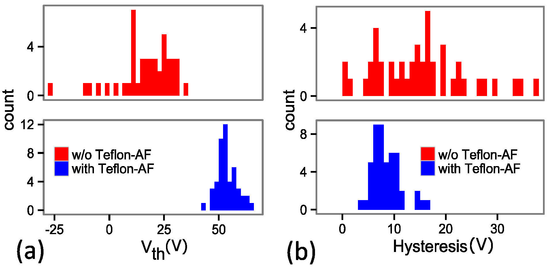
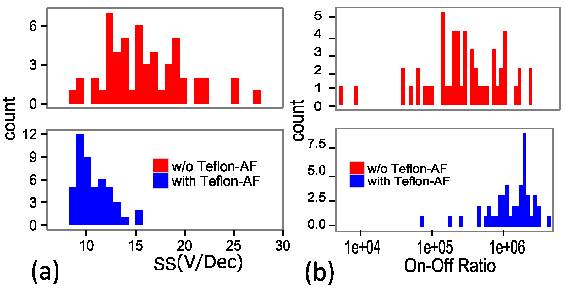
All of the devices of this work were fabricated on P+ silicon bottom gate with 300 nm-thick thermally grown SiO2 that was used as the gate dielectric. Monolayer MoS2 was grown on the substrate using a CVD process explained elsewhere [10]. An optical images of CVD MoS2 crystal grown on 300 nm SiO2 is shown in Figure 1a. The monolayer structure of the grown CVD films were confirmed by Raman and photoluminescence (PL) spectroscopy shown in Figure 2. The E 2 g 1 and A 1 g peaks are at 389.3 cm−1 and 409.1 cm−1, respectively. This corresponds to a peak separation of 19.8 cm−1, which is characteristic of single-layer MoS2 [24]. The PL spectrum of the CVD MoS2 also shows a strong peak at around 685 nm which corresponds to monolayer MoS2 [25].
A conventional photolithography process was used to define the channels and contacts. The channels were isolated using Cl2 plasma followed by patterning and deposition of source/drain contacts (20 nm Ag/ 20 nm Pd). The fabricated two-probe devices have a constant width of 3 μm and a variable length of 3 μm, 6 μm and 9 μm. An optical image of the MoS2 FET with channel dimensions of 3 μm × 9 μm, is shown in Figure 1b.
The initial electrical characteristics of about 60 randomly-chosen devices distributed on a 5 mm × 5 mm surface area were tested under room ambient conditions. The field-effect modulation of CVD MoS2 FETs were studied by sweeping the back-gate bias in [−100, 100] V range. Afterwards, the sample was held in N2 glovebox for half an hour, before being coated with Teflon-AF (Dupont Co., Wilmington, NC, USA). Vacuum and N2 environment were previously reported to be equally efficient in removing the adsorbates from unpassivated back-gated MoS2 devices [26]. In the next step, 140 nm Teflon-AF encapsulation cap was spin-coated on the sample with as-supplied Teflon-AF solution at 2000 rpm for 1 min. The sample was then placed on the hotplate and cured at 250 °C for 30 mins in N2 ambient. After the cure step, the hotplate temperature was reduced to room temperature with a ramp rate of 20 °C/min. Teflon-AF is a soluble fluoropolymer in selected solvents, based on copolymers of 2,2-bistrifluoromethyl-4,5-difluoro-1,3-dioxole (PDD) and tetrafluoroethylene (TFE) [27]. Teflon-AF is known to have a high-polarity amorphous structure, which is originated from a number of C-F bonds in it, with a dipole moment of 1.13D [28]. Raman and photoluminescence characterization were used to check any structural and material changes in MoS2 monolayer after applying the Teflon-AF cap. Figure 2a,b compares the Raman and PL scattering of MoS2 before and after applying the cap. The attenuated intensity of signal in both cases is likely due to the thickness of the cap.

3. Results

Figure 3a,b compares the electrical transfer characteristics of 15 representative devices before and after treating the surface with Teflon-AF. No drain saturation current is observed in both cases due to the thick back gate dielectric. A large variability of the device performance is observed in Figure 3a before applying the Teflon cap. This variability, which may be caused by the charges trapped between the channel and gate dielectric or the moisture and oxygen molecules adsorbed on the surface of channel, is reduced in Figure 3b after applying the cap. These changes can be explained by first, the hydrophobic nature of Teflon-AF that significantly reduces the charges adsorbed on the channel surface. Second, neutralization of charge traps, within the channel and at the interface of channel and gate dielectric, by the local electric field induced in Teflon-AF. This local electric field could screen the scattering impact of trapped charges between the channel and gate dielectric. The impact of the reduction of adsorbates on the surface of the channel shows up in the form of reduced gate hysteresis, observed in all tested devices and presented in Figure 4a. For the specific device presented here, the hysteresis is reduced from ~25 V to ~10 V. The reduction of the gate hysteresis has been reported previously for devices tested under vacuum and those tested after long-term vacuum annealing steps. Note that in none of these cases the hysteresis is reduced to zero. This is believed to be due to the remaining oxygen to be strongly bonded to the defects and edges of the MoS2 channel [18]. Improvement in the off-current states upon coating with Teflon-AF is possibly due to the polar molecules of the fluoropolymer which will partially neutralize charged dopants [22,29].
Figure 4b compares the transfer characteristics of the same device in the linear scale before and after applying the cap. The threshold voltage (Vth) is calculated from the x-intercept of the linear fit in the strong inversion region (dotted lines in Figure 4b). The positive shift in Vth, observed in all measured devices after applying the cap, is attributed to the net impact of the local dipole electric field and the back gate electric field. Since MoS2 works like an n-type FET, this leads to a lower density of carriers in the device channel. The inset in Figure 4b shows the drain current (Id) for the same overdrive gate bias. The reduction of Id at the same overdrive gate bias after applying the cap, is likely due to the local electric field caused by the alignment of the dipoles of the cap. As a result of this local electric field the density of the charge carriers and the drain current decreases.
In order to study the impact of Teflon-AF, approximately 60 devices were tested under ambient conditions before and after applying the cap. The distribution of threshold voltage (Vth), gate hysteresis, subthreshold swing and current on-off ratio of the tested devices are shown in Figure 5a,b and Figure 6a,b. The average value of the Vth shifts from 15.8 V to 58 V after applying the cap. This leads to about two orders of magnitude reduction of the drain current at Vg = 0 V and effectively turning off the MoS2 FET at zero back gate bias.
Figure 5b presents the distribution of gate hysteresis. The hysteresis is calculated by taking the difference between the Vth when Vg is swept from negative to positive direction and vice versa. An improvement was observed in both the average and the standard deviation of the gate hysteresis distribution after applying the cap. The average value reduces from 15.1 V to 8 V. The gate hysteresis is mainly caused by the trapped mobile charges present within the gate dielectric and at the interface of the channel that rearrange under gate bias and drain voltage. The polar structure of Teflon-AF proved significantly effective in neutralizing the mobile charge traps.
Figure 6a presents the subthreshold swing (SS) of tested devices calculated using, S S = l n 10 d V g d l n ( I d ) . The average value of SS reduces from 15.9 V/Dec and 10.7 V/Dec after applying the cap. This reduction is in agreement with reduced charge transfer between the surface adsorbates and channel carriers. The reduction of the standard deviation of all three performance metrics here shows an improved device to device consistency.
Figure 6b presents the improved on-off switching ratio after applying Teflon-AF. The average value changes from 5 × 10⁵ to 2 × 10⁶ after applying the cap, showing a significant improvement of off-current state.

4. Conclusions

In conclusion, we report the improved performance of MoS2 FETs by applying a fluoropolymer capping layer. Our results show a significant improvement in device performance variability, gate hysteresis, subthreshold swing and on-off ratio. These improvements are attributed to desorption of ambient adsorbates from the surface of the channel and the gate dielectric and also the polar nature of the fluoropolymer that neutralizes the impact of charge impurities.

Acknowledgments

This work was supported in part by the NSF CAREER award (D.A.), the NSF-NASCENT Engineering Research Center (Cooperative Agreement No. EEC-1160494), and the Nanoelectronics Research Initiative (NRI) Southwest Academy of Nanoelectronics (SWAN) Center. The fabrication was conducted at the Microelectronics Research Center (MRC) at the University of Texas at Austin, which is a member of the National Nanotechnology Coordinated Infrastructure Network (NNCI).

Author Contributions

S.R. and R.G. contributed equally to this work. S.R. and R.G. conceived and designed the experiments; R.G. was responsible for material synthesis and characterization, S.R. was responsible for device fabrication, characterization and analysis. S.K. was responsible for fluoropolymer application to the transistors. S.R., R.G., S.K., A.D., S.B. and D.A. wrote the manuscript together.

Conflicts of Interest

The authors declare no conflict of interest.

References

  1. Frey, G.L.; Elani, S.; Homyonfer, M.; Feldman, Y.; Tenne, R. Optical-absorption spectra of inorganic fullerenelike MS2. Phys. Rev. B 1998, 57. [Google Scholar] [CrossRef]
  2. Mak, K.F.; Lee, C.; Hone, J.; Shan, J.; Heinz, T.F. Atomically thin MoS2: A new direct-gap semiconductor. Phys. Rev. Lett. 2010, 105. [Google Scholar] [CrossRef] [PubMed]
  3. Cao, T.; Wang, G.; Han, W.P.; Ye, H.Q.; Zhu, C.R.; Shi, J.R.; Niu, Q.; Tan, P.H.; Wang, E.; Liu, B.L.; et al. Valley-selective circular dichroism of monolayer molybdenum disulphide. Nat. Commun. 2012, 3. [Google Scholar] [CrossRef] [PubMed]
  4. Bhimanapati, G.R.; Lin, Z.; Meunier, V.; Jung, Y.; Cha, J.J.; Das, S.; Xiao, D.; Son, Y.; Strano, M.S.; Cooper, V.R.; et al. Recent advances in two-dimensional materials beyond graphene. ACS Nano 2015, 9, 11509–11539. [Google Scholar] [CrossRef] [PubMed]
  5. Radisavljevic, B.; Whitwick, M.B.; Kis, A. Integrated circuits and logic operations based on single-layer MoS2. ACS Nano 2011, 5, 9934–9938. [Google Scholar] [CrossRef] [PubMed]
  6. Radisavljevic, B.; Whitwick, M.B.; Kis, A. Small-signal amplifier based on single-layer MoS2. Appl. Phys. Lett. 2012, 101. [Google Scholar] [CrossRef]
  7. Zeng, H.; Dai, J.; Yao, W.; Xiao, D.; Cui, X. Valley polarization in MoS2 monolayers by optical pumping. Nat. Nanotechnol. 2012, 7, 490–493. [Google Scholar] [CrossRef] [PubMed]
  8. Ghorbani-Asl, M.; Zibouche, N.; Vahiduzzaman, M.; Oliveira, A.F.; Kuc, A.; Heine, T. Electromechanics in MoS2 and WS2: Nanotubes vs. monolayers. Sci. Rep. 2013, 3. [Google Scholar] [CrossRef] [PubMed]
  9. Nayak, A.P.; Pandey, T.; Voiry, D.; Liu, J.; Moran, S.T.; Sharma, A.; Tan, C.; Chen, C.H.; Lee, L.J.; Chhowalla, M.; et al. Pressure-dependent optical and vibrational properties of monolayer molybdenum disulfide. Nano Lett. 2015, 15, 346–353. [Google Scholar] [CrossRef] [PubMed]
  10. Sanne, A.; Ghosh, R.; Rai, A.; Yogeesh, M.N.; Shin, S.H.; Sharma, A.; Jarvis, K.; Mathew, L.; Rao, R.; Akinwande, D.; Banerjee, S. Radio frequency transistors and circuits based on CVD MoS2. Nano Lett. 2015, 15, 5039–5045. [Google Scholar] [CrossRef] [PubMed]
  11. Chang, H.-Y.; Yogeesh, M.N.; Ghosh, R.; Rai, A.; Sanne, A.; Yang, S.; Lu, N.; Banerjee, S.; Akinwande, D. Large-area monolayer MoS2 for flexible low-power RF nanoelectronics in the GHz regime. Adv. Mater. 2016, 28, 1818–1823. [Google Scholar] [CrossRef] [PubMed]
  12. Rahimi, S.; Tao, L.S.N.; Chowdhury, Sk.F.; Park, S.; Jouvray, A.; Buttress, S.; Rupesinghe, N.; Teo, K.; Akinwande, D. Toward 300 mm wafer-scalable high-performance polycrystalline chemical vapor deposited graphene transistors. ACS Nano 2014, 8, 10471–10479. [Google Scholar] [CrossRef] [PubMed]
  13. Kang, K.; Xie, S.; Huang, L.; Han, Y.; Huang, P.Y.; Mak, K.F.; Kim, C.J.; Muller, D.; Park, J. High-mobility three-atom-thick semiconducting films with wafer-scale homogeneity. Nature 2015, 520, 656–660. [Google Scholar] [CrossRef] [PubMed]
  14. Wang, H.; Wu, Y.; Cong, C.; Shang, J.; Yu, T. Hysteresis of electronic transport in graphene transistors. ACS Nano 2010, 4, 7221–7228. [Google Scholar] [CrossRef] [PubMed]
  15. Franklin, A.D.; Tulevsky, G.S.; Han, S.J.; Shahrjerdi, D.; Cao, Q.; Chen, H.Y.; Wong, H.-S.P.; Haensch, W. Variability in carbon nanotube transistors: Improving device-to-device consistency. ACS Nano 2012, 6, 1109–1115. [Google Scholar] [CrossRef] [PubMed]
  16. Davis, S.M.; Carver, J.C. Oxygen chemisorption at defect sites in MoS2 and ReS2 basal plane surfaces. Appl. Surf. Sci. 1984, 20, 193–198. [Google Scholar] [CrossRef]
  17. Jaegermann, W.; Schmeisser, D. Reactivity of layer type transition metal chalcogenides towards oxidation. Surf. Sci. 1986, 165, 143–160. [Google Scholar] [CrossRef]
  18. Qiu, H.; Pan, L.; Yao, Z.; Li, J.; Shi, Y.; Wang, Z. Electrical characterization of back-gated bi-layer MoS2 field-effect transistors and the effect of ambient on their performances. Appl. Surf. Sci. 2012, 100. [Google Scholar] [CrossRef]
  19. Chowdhury, Sk.F.; Sonde, S.; Rahimi, S.; Tao, L.; Banerjee, S.; Akinwande, D. Improvement of graphene field-effect transistors by hexamethyldisilazane surface treatment. Appl. Surf. Sci. 2014, 105. [Google Scholar] [CrossRef]
  20. Lafkioti, M.; Krauss, B.; Lohmann, T.; Zschieschang, U.; Klauk, H.; Klitzing, K.V.; Smet, J.H. Graphene on a hydrophobic substrate: Doping reduction and hysteresis suppression under ambient conditions. Nano Lett. 2010, 10, 1149–1153. [Google Scholar] [CrossRef] [PubMed]
  21. Ha, T.J.; Lee, J.; Chowdhury, Sk.F.; Akinwande, D.; Rossky, P.J.; Dodabalapur, A. Transformation of the electrical characteristics of graphene field-effect transistors with fluoropolymer. ACS Appl. Mater. Interfaces 2012, 5, 16–20. [Google Scholar] [CrossRef] [PubMed]
  22. Jang, S.; Kim, B.; Geier, M.L.; Prabhumirashi, P.L.; Hersam, M.C.; Dodabalapur, A. Fluoropolymer coatings for improved carbon nanotube transistor device and circuit performance. Appl. Surf. Sci. 2014, 105. [Google Scholar] [CrossRef]
  23. Kim, J.; Liu, Y.; Zhu, W.; Kim, S.; Wu, D.; Tao, L.; Dodabalapur, A.; Lai, K.; Akinwande, D. Toward air-stable multilayer phosphorene thin-films and transistors. Sci. Rep. 2015, 5. [Google Scholar] [CrossRef] [PubMed]
  24. Lee, Y.; Zhang, X.; Zhang, W.; Chang, M.; Lin, C.; Chang, K.; Yu, Y.; Wang, J.; Chang, C.; Li, L.; et al. Synthesis of large-area MoS2 atomic layers with chemical vapor deposition. Adv. Mater. 2012, 24, 2320–2325. [Google Scholar] [CrossRef] [PubMed]
  25. Splendiani, A.; Sun, L.; Zhang, Y.; Li, T.; Kim, J.; Chim, C.Y.; Galli, G.; Wang, F. Emerging photoluminescence in monolayer MoS2. Nano Lett. 2010, 10, 1271–1275. [Google Scholar] [CrossRef] [PubMed]
  26. Tavana, H.; Hair, M.L.; Neumann, A.W. Influence of electronic properties of naphthalene compounds on contact angles. J. Phys. Chem. B 2006, 110, 1294–1300. [Google Scholar] [CrossRef] [PubMed]
  27. Yang, M.K.; French, R.H.; Tokarsky, E.W. Optical properties of Teflon® AF amorphous fluoropolymers. J. Micro/Nanolithogr. MEMS MOEMS 2008, 7. [Google Scholar] [CrossRef]
  28. Park, W.; Park, J.; Jang, J.; Lee, H.; Jeong, H.; Cho, K.; Hong, S.; Lee, T. Oxygen environmental and passivation effects on molybdenum disulfide field effect transistors. Nanotechnology 2013, 24. [Google Scholar] [CrossRef] [PubMed]
  29. Namgung, S.D.; Yang, S.; Park, K.; Cho, A.-J.; Kim, H.; Kwon, J.-Y. Influence of post-annealing on the off current of MoS2 field-effect transistors. Nanoscale Res. Lett. 2015, 10. [Google Scholar] [CrossRef] [PubMed]
Figure 1. (a) Optical microscope (Olympus, Tokyo, Japan) image of chemical vapor deposited (CVD) MoS2 crystals; (b) An image of the MoS2 field effect transistors (FET) with channel dimensions of 3 μm × 9 μm.
Applsci 06 00236 g001
Figure 2. (a) Raman spectrum of MoS2 before (red) and after (blue) applying Teflon-AF encapsulation layer; (b) photoluminescence (PL) spectrum of monolayer MoS2 before (red) and after (blue) applying the cap.
Applsci 06 00236 g002
Figure 3. Transfer characteristics of representative FETs before (a); and after (b) applying Teflon-AF. The y-axis is Id in nA unites for both cases and the dotted lines are visual guides emphasizing the Vth shift after applying the polymer cap.
Applsci 06 00236 g003
Figure 4. (a) Transfer curves shows a reduction in the gate hysteresis and the desirable enhancement mode character of the transistor after applying the polymer cap; (b) Transfer curves plotted in the linear scale shows a positive Vth shift after applying the polymer cap that could be explained either by the trapped charges between the cap and channel or hole doping of the channels. The inset shows reduction of off-state current and slight improvement of on-state current at high overdrive gate bias after applying the cap.
Applsci 06 00236 g004
Figure 5. Histogram distribution of (a) threshold voltage; (b) gate hysteresis of 60 measured devices before and after applying Teflon-AF cap.
Applsci 06 00236 g005
Figure 6. Histogram distribution of (a) subthreshold swing; and (b) On-Off ratio of 60 measured devices before and after applying Teflon-AF cap presented in a log-scale x-axis.
Applsci 06 00236 g006

