SNR Enhancement of an Electrically Small Antenna Using a Non-Foster Matching Circuit


1
Department of Electrical and Information Engineering; SeoulTech, Seoul 01811, Korea
2
Department of Manufacturing Systems and Design Engineering; SeoulTech, Seoul 01811, Korea
*
Author to whom correspondence should be addressed.
Appl. Sci. 2020, 10(13), 4464; https://doi.org/10.3390/app10134464
Submission received: 2 June 2020
/
Revised: 23 June 2020
/
Accepted: 24 June 2020
/
Published: 28 June 2020
(This article belongs to the Collection Electromagnetic Antennas for HF, VHF, and UHF Band Applications)
Abstract
:Featured Application
Miniaturized broadband antennas for wireless communication devices
Abstract
A non-Foster circuit (NFC) is known as an active broadband matching technique to improve the impedance matching bandwidth of an electrically small antenna (ESA). There has been a vast amount of papers that report the generation of negative impedance using an NFC and its effectiveness on broadband antenna matching. However, only a few discussed its impact on the signal-to-noise-ratio (SNR), which is one of the most important figures-of-merit for a wireless communication system. In this paper, the SNR enhancement due to an NFC was measured and discussed. An NFC was carefully designed to have a low dissipation loss and to meet the stability conditions. The optimized NFC design was fabricated and applied to an ESA length of λ⁄15 at a frequency range of 150 to 300 MHz. The measured results showed that the NFC enhanced the received power of the antenna system by more than 17 dB. However, due to the noise added by the NFC, the SNR enhancement was not guaranteed for some frequency points. Nevertheless, an average of 7.3 dB of SNR improvement over the frequency band of interest is possible based on the experiment result.
1. Introduction
The demand for miniaturized communication systems has tremendously increased for many applications such as mobile devices, medical wearables, military radios and vehicles, etc. One of the key components that prohibit the miniaturization is an antenna because of its physical length (or area) requirement, depending on the frequency. For example, the ideal length of a quarter-wavelength antenna operating at 300 MHz is 25 cm. No matter how small the design of the circuit or chassis is, the size of the whole communication system is big due to the antenna.
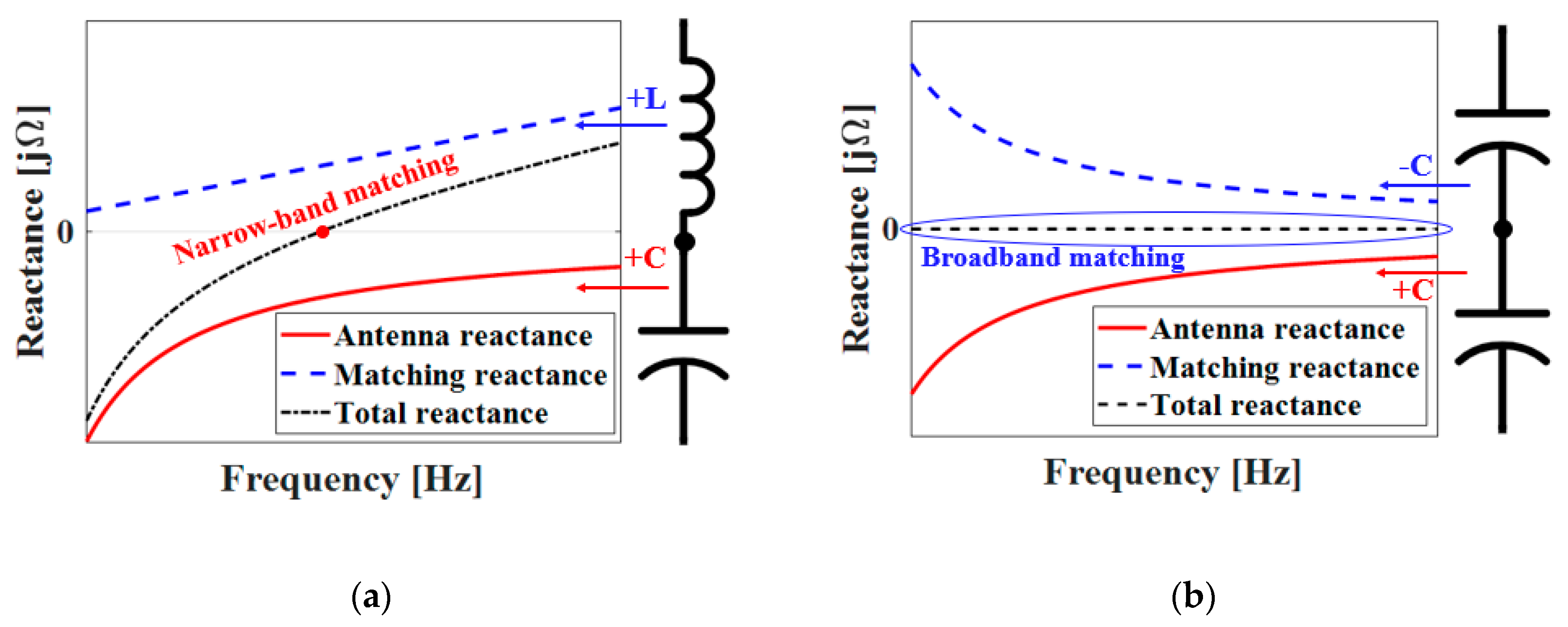
For the last decade, a vast amount of research has been conducted on the so-called electrically small antenna (ESA), which is defined by an antenna whose maximum dimension is less than [1,2]. Although an ESA presents a small footprint, it usually accompanies low radiation resistance and high reactance, which makes it difficult to match to the system impedance (e.g., ). To promote the impedance matching, often passive components, such as inductors (L) and capacitors (C), are used to remove the reactance at a designated frequency band. However, the matching bandwidth is extremely narrow, since the passive L, C, and the antenna itself follow the Foster’s reactance theorem [3]. The latter asserts that the reactance must increase as the frequency increases.
Figure 1a shows an example of adjusting the reactance of a capacitive ESA using an inductor. Both the C and L increase as the frequency increases, following Foster’s reactance theorem. The ESA’s capacitance is completely cancelled by the inductance at a single frequency, implying the matching bandwidth is narrow. To overcome the bandwidth limitation of passive impedance matching, a non-Foster circuit (NFC) matching technique employing active components (e.g., transistor) has been introduced [4,5]. The operation principle of an NFC is simple, as depicted in Figure 1b. It generates a negative C (or L), which is against the Foster’s reactance theorem, and thus a broad reactance cancellation bandwidth can be achieved. Various non-Foster circuit designs have been reported for the broadband matching of small antennas [6,7,8,9,10,11]. However, most of them presented only the enhancement in the antenna’s reflection coefficient () after applying the NFC, which is not sufficient to validate the system-wide improvement. It is important to examine the signal-to-noise ratio (SNR) since the active components employed in the NFC might introduce additional noise into the system [12,13].
In this paper, an NFC design with improved matching bandwidth and stability is presented. Compared to the previously designed NFC [6], this work has a much smaller footprint by shortening the microstrip line, and thus the overall loss and parasitic effect originating from the NFC can be reduced. More importantly, not only the impedance enhancement, but the received power and SNR enhancement after applying the NFC, is presented and discussed. The NFC was carefully designed, focusing on the reduction of internal loss, resulting in an average of 17.3 dB of received power improvement in the bandwidth of 150 to 300 MHz. To improve the stability of the NFC, a two-step validation check strategy of observing the stability condition in both frequency and time domains was applied. The NFC design is described in detail in Section 2. The noise power added by the implemented NFC was measured and the overall SNR enhancement was calculated. The results show that the proposed NFC provides an average of 7.3 dB of enhancement of SNR despite of the introduced noise. These measured results are discussed in Section 3.
2. Non-Foster Circuit Design
This section first introduces the ESA used in this study. This is important since the NFC design strongly depends on the impedance of the ESA connected with it. Next, the proposed NFC design is discussed together with the stability validation methods and their simulation results.
2.1. Characteristics of Electrically Small Antenna
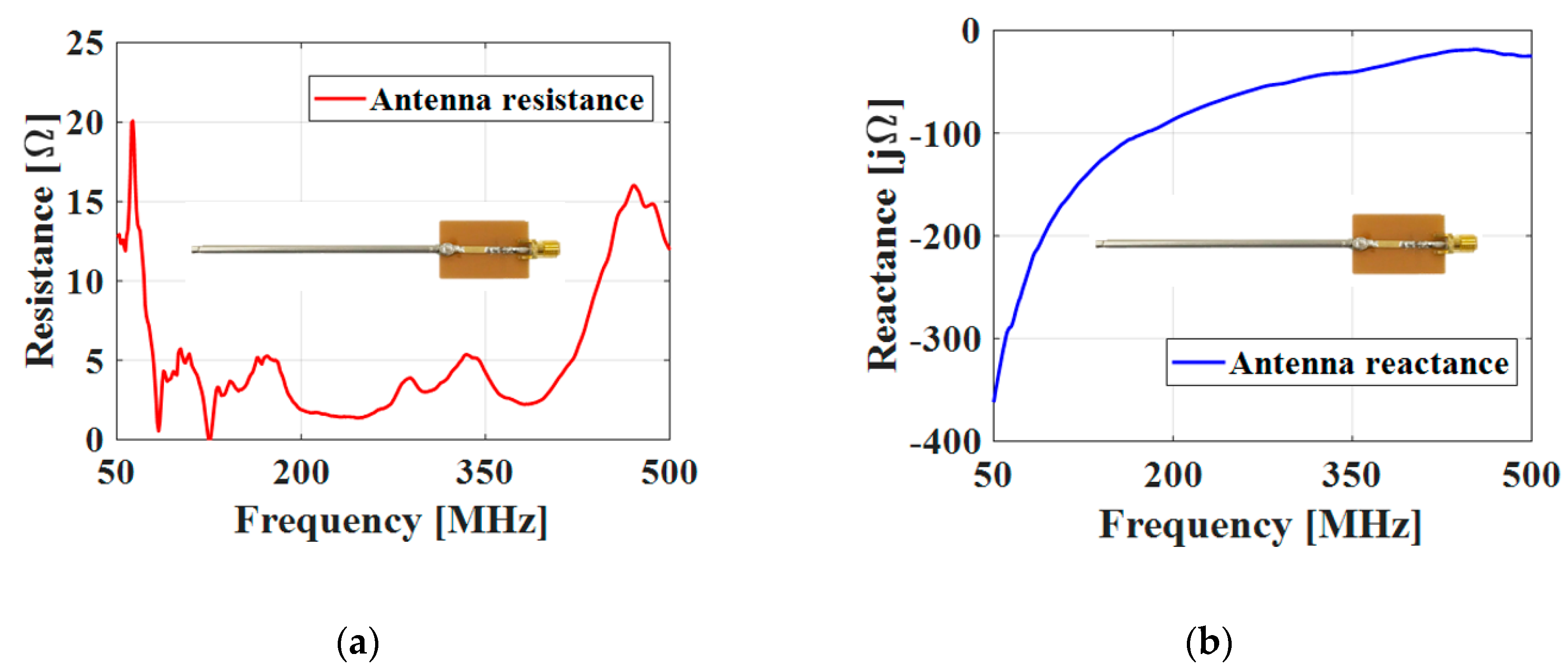
A short monopole was selected as the load. Figure 2 shows its measured resistance and reactance together with a picture of the monopole. The length of the monopole is 8.4 cm, corresponding to the quarter-wavelength of 893 MHz. Thus, it can be considered as an ESA at the frequency of interest (i.e., 150–300 MHz). The measured resistance and reactance in Figure 2a,b, respectively, clearly display impedance characteristics of an ESA: the resistance is low and reactance is high. One can easily notice that the reactance behavior is similar to Figure 1a: the negative reactance reduces as the frequency increases in a rational manner. This means that as the frequency increases, the negative value of the capacitive reactance decreases (i.e., ).
The purpose of the NFC is to generate a negative capacitance complimentary to the antenna’s positive capacitance, and therefore, the input reactance can be 0 over a wide bandwidth. More specifically, the antenna capacitance of 8 ± 1 pF can be cancelled by the NFC’s negative capacitance of −8 ∓ 1 pF.
2.2. Non-Foster Circuit Design
Figure 3 shows the schematic of the proposed non-Foster circuit to provide negative capacitance. Two transistors are cross-coupled to produce a 180-degree inverted phase from the input along the feedback loop [5]. The transistors used were Avago ATF-53189 [14], which are field effect transistors with wideband operation bandwidths of 50 MHz–6.5 GHz. With these basic schematics and selected transistors, the other components were optimized to satisfy the stability condition described in Section 2.3. A high frequency circuit simulator, Keysight Technologies Advanced Design System (ADS) [15], was used for the optimization. Table 1 lists the optimized values of other components. The reference impedance (Zref) of the NFC was set to 6 pF considering the monopole’s capacitance. The values of inductors (LG, LD, LS) and resistors (RG, RD, Rs) connected to the gate, drain, and source of the transistors should be carefully chosen to ensure the wideband stability criterion. As the value of the inductor increases, its self-resonant frequency (SRF) decreases, adversely affecting the NFC stability [16]. The resistor values are also important since the wrong selection can lead to a generation-negative resistance that goes against the stability condition [17]. To reduce the loop gain of the transistors for stability, RStab and CStab are set as 51 Ω, 1 pF, respectively. The gate voltage (VGG), drain voltage (VDD), and drain current of the designed circuit are 1.8 V, 5.7 V, and 4 mA, respectively.
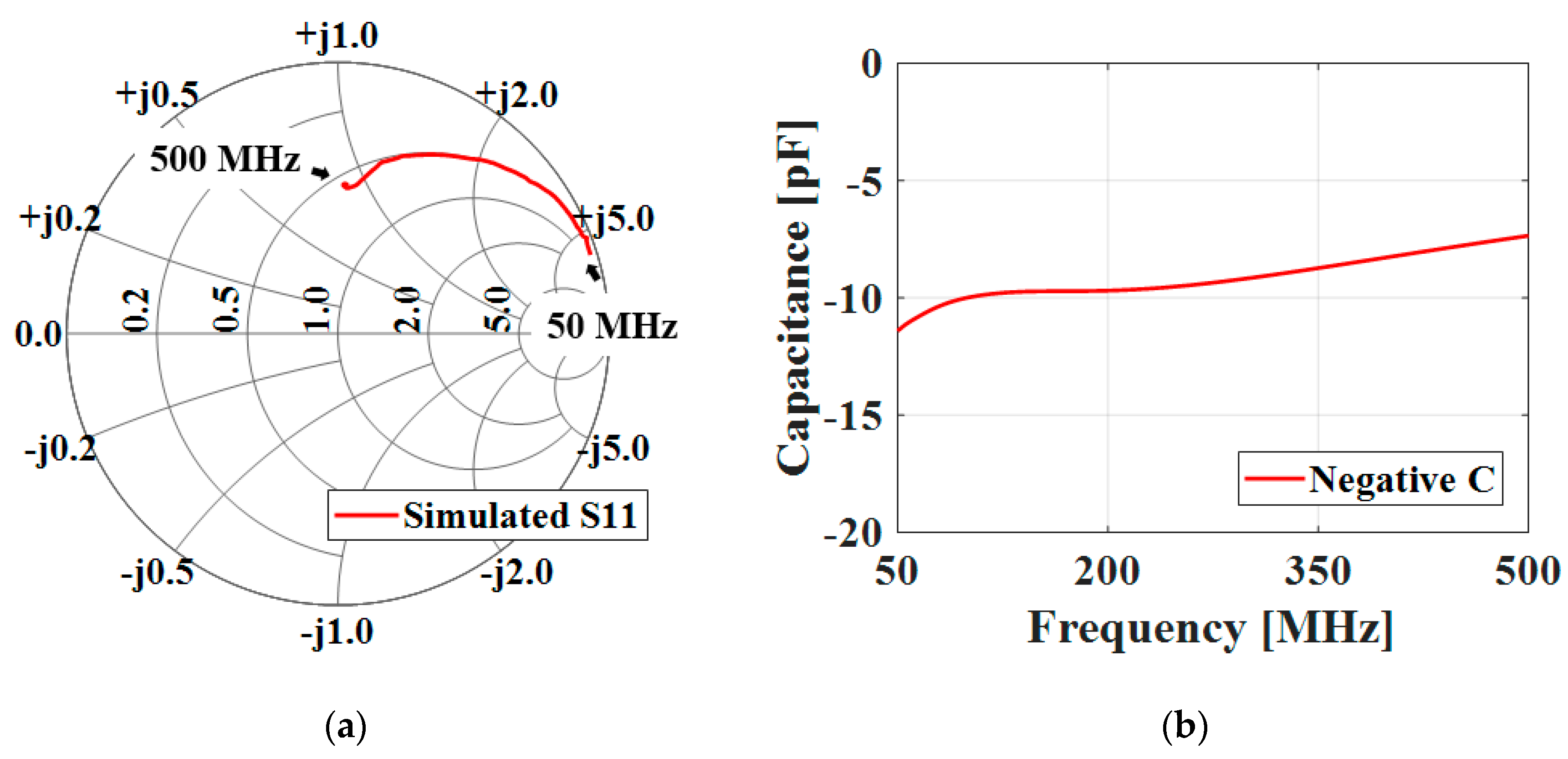
Figure 4 shows the simulated results of the NFC in the frequency range from 50 MHz to 500 MHz. According to the Smith chart of the reflection coefficient () in Figure 4a, the locus winds in a counterclockwise manner as the frequency increases from 50 MHz to 500 MHz. This contradicts the Foster’s reactance theorem, denoting that the negative capacitance has been successfully generated. Figure 4b plots the capacitance versus the frequencies. As can be seen, a negative capacitance ranging from 11 pF to 7.5 pF, and approximately 8 pF at 300 MHz, is generated.
2.3. Non-Foster Circuit Stability Check
In common stability criteria for a 2-port network such as the Llewellyn-Rollett port test, the network is stable if there are no internal poles or zeros in the right-hand plane (RHP) for a complex plane analysis [18]. However, this is not the case for an NFC since the negative impedance often provides poles and zeros in the RHP. Instead, the stability of an NFC is often tested by checking the short-circuit stability (SCS) or open-circuit stability (OCS) conditions. For the NFC connected with an antenna, the OCS condition is applied [5], and can be written as
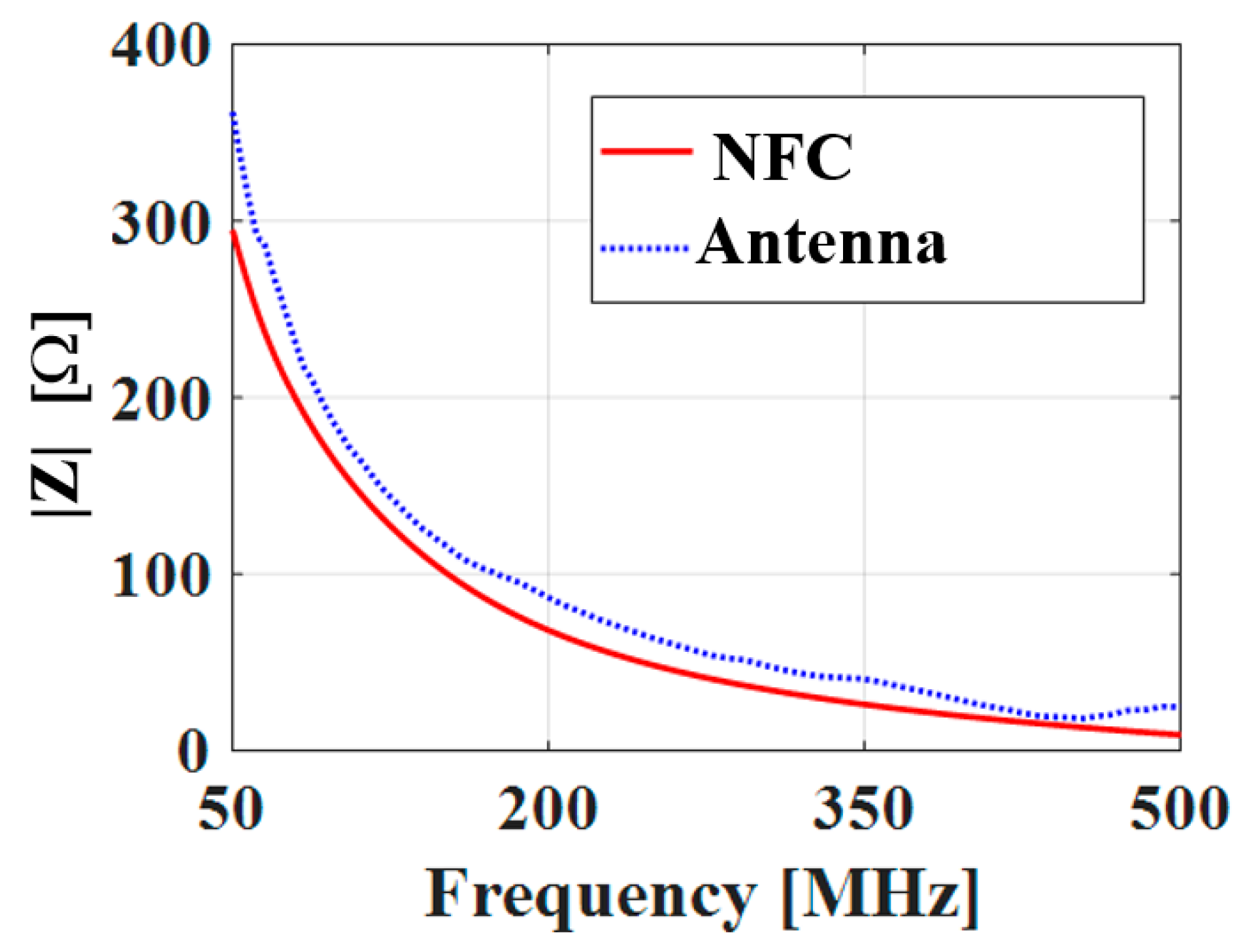
where |ZAnt| and |ZNFC| are the magnitudes of the antenna and NFC impedance. This condition must be satisfied throughout the frequency band of interest where the NFC generates the negative impedance. Figure 5 shows |ZAnt| > |ZNFC| in the frequency range of 50–500 MHz for the proposed NFC. It is observed that the OCS criterion in (1) is satisfied.
|ZAnt| > |ZNFC|,
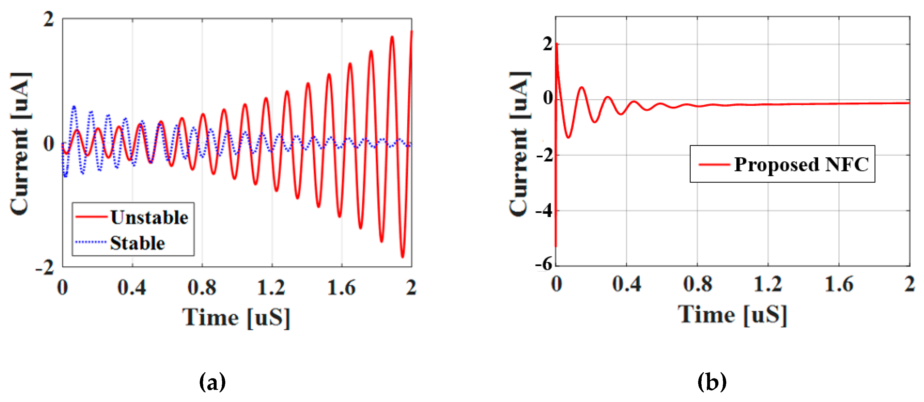
However, the OCS criterion assumes the network is dispersionless. In fact, no circuit is dispersionless in the real world. There is unavoidable coupling between transmission lines and parasitic components that can cause undesirable small oscillations and possibly diverge as the currents travel through the NFC’s feedback loop. Thus, it is important to check the transient response in the time domain [16,18] in addition to the OCS criterion in the frequency domain. By observing the transient response, the sign of the time constants () can be identified. If the sign of is negative, the circuit is unstable and the transient response diverges as illustrated in Figure 6a. However, if the sign of is positive, the transient response damps down and converges as the time passes (Figure 6a). The transient response of the proposed NFC is shown in Figure 6b. Depending on the combinations of resistor-inductor-capacitor (RLC) components, some NFC designs satisfied the OCS criterion but failed to demonstrate convergence for the transient response. The optimized RLC values in Table 1 satisfy both the OCS and transient response requirements.
3. Fabrication and Measurement of Non-Foster Circuit
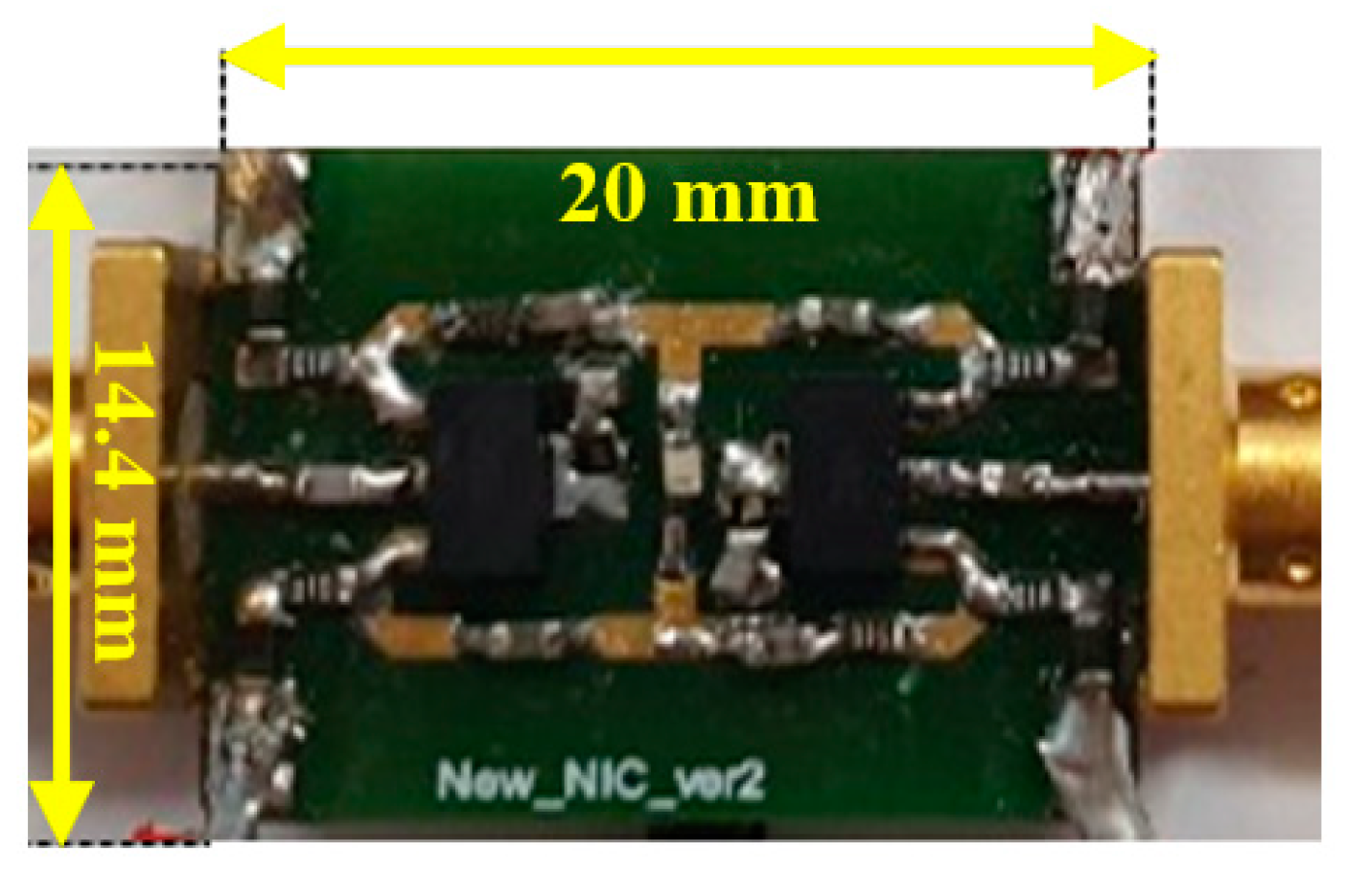
Having validated the NFC performance using simulations, the optimized NFC was fabricated as shown in Figure 7. It was implemented on an FR-4 substrate with a footprint of 14.4 mm × 20 mm, which is smaller than the previous report [6]. It was miniaturized by reducing the length of microstrip lines connecting the transistors and RLC components. This also reduced the overall losses consumed by the NFC, resulting in the use of lower R values to satisfy the stability conditions.
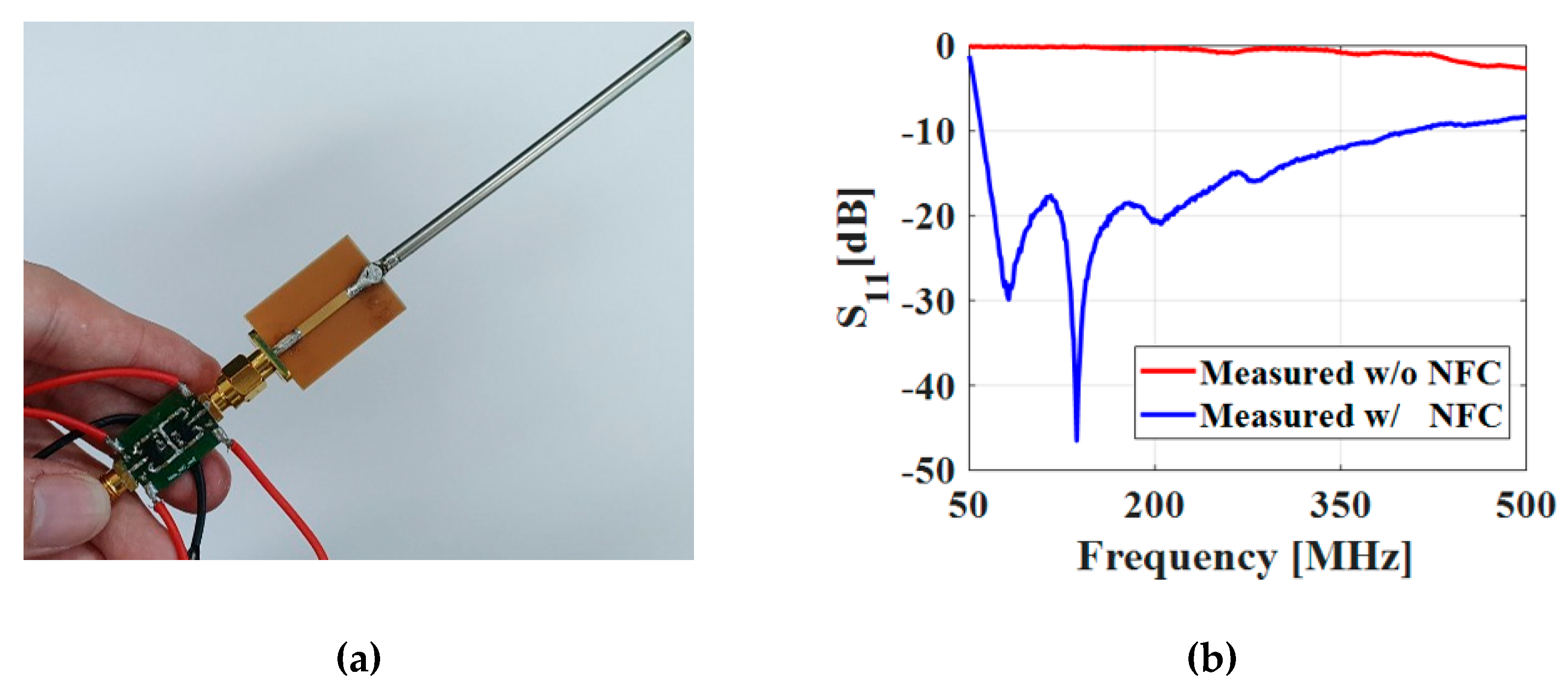
3.1. Measurement of Reflection Coefficient
Figure 8a is a picture of the small monopole and NFC assembly. A network analyzer (Anritsu MCS2038C) was connected to the input port of the NFC to measure the . The measured is shown in Figure 8b. The comparison made here is with and without the NFC. The latter means the monopole was directly connected to the network analyzer. As observed, the measured without the NFC is higher than –2 dB over the whole frequency range, 50–500 MHz. This is due to the high capacitance preventing the monopole from reaching the resonance as described in Section 2.1. Contrarily, the dB bandwidth is 60–400 MHz when the NFC is connected to the monopole. This proves that the NFC successfully removes the positive capacitance of the monopole by generating a sufficient amount of negative capacitance.
3.2. Measurement of Signal-to-Noise Ratio
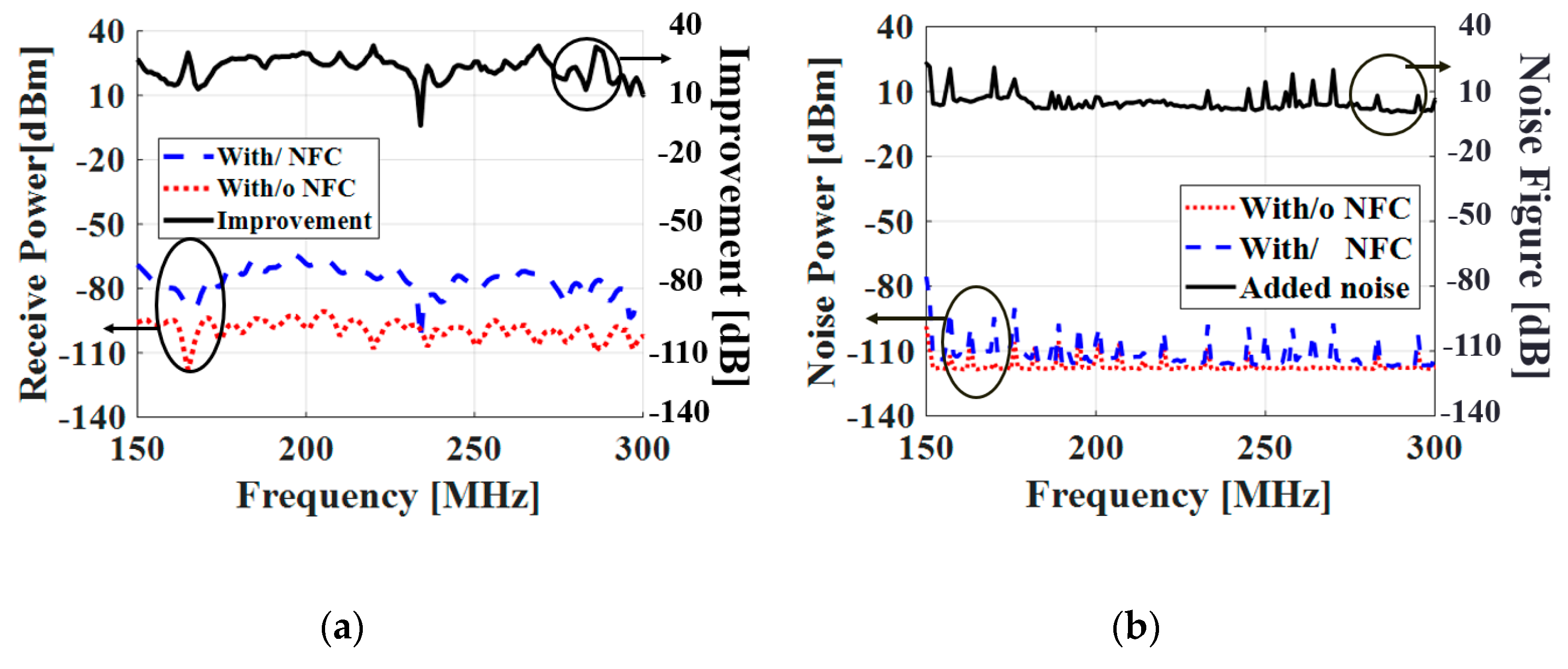
As described in the introduction, the broadband does not guarantee the effectiveness of the NFC since the NFC itself can generate additional noise that may adversely influence a systematical figure-of-merit, SNR. With this issue in mind, we proceeded to measure SNR with and without the NFC, following the measurement setups depicted in Figure 9. The transmitted signals, originated by a signal generator, were captured by a spectrum analyzer in the receiving end. The received power and noise power read by the spectrum analyzer are denoted as (SESA, NESA) without the NFC and (SESA+NFC, NESA+NFC) with the NFC, respectively. With them, the SNR enhancement due to the NFC can be calculated by
means Received power enhancement, and ) means Added noise.
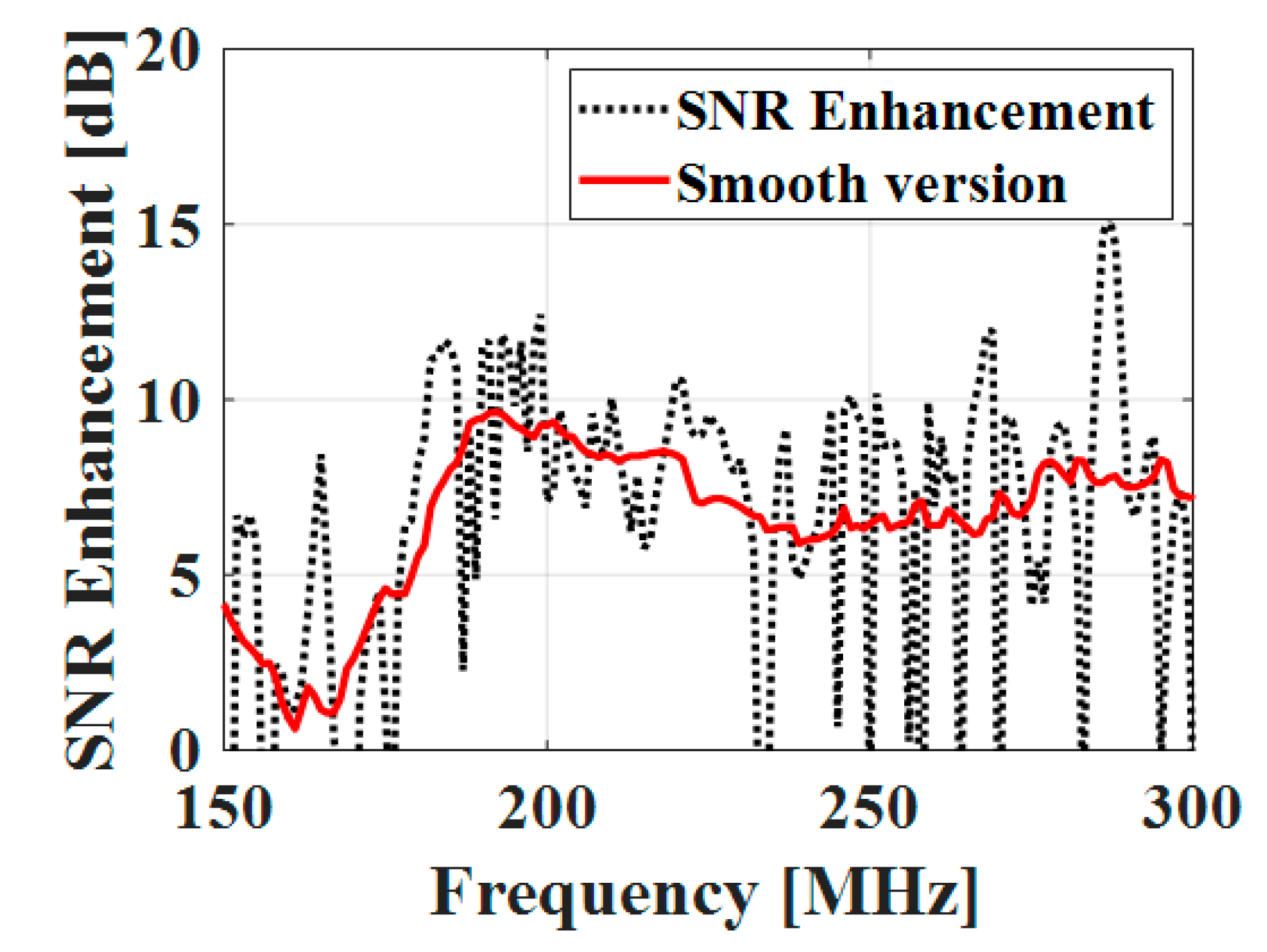
Figure 10a shows the received power recorded by the spectrum analyzer with and without the NFC. Their difference is labelled as “Improvement”. There are some fluctuations, but the power received with the NFC equipped shows higher values than the antenna-only case (i.e. without the NFC) throughout the frequency range of 150–300 MHz. The average power improvement achieved by using the NFC is 17.3 dB. Subsequently, Figure 10b shows the noise power added by the NFC. It can be observed that the NFC adds fluctuating noise, which peaks at more than 7 dB for some frequency points. These fluctuations come from the thermal noise increase and decrease as the currents travel in the feedback loop of the NFC. The added noise base is around 7 dB, and for the noise-peaking frequencies, it is around 14 dB. Finally, the SNR enhancement by the NFC was calculated by subtracting the received power enhancement from the added noise power. As depicted in Figure 11, the SNR enhancement values also significantly fluctuate due to the noise fluctuation, implying that the NFC is not effective in improving the reception of the communication system for certain frequencies. The fluctuation does not exceed the stability limit but can adversely affect the SNR of the system. Figure 11 also shows a smoothed curve of SNR enhancement. It indicates that an average of 7.2 dB of SNR enhancement can be achieved if the noise fluctuation can be controlled by implementing a cooling or damping device on the NFC.
4. Conclusions
A non-Foster circuit was designed to improve the SNR of an electrically small monopole antenna. The cross-coupled structure of the NFC was optimized using a high frequency circuit simulation software, Keysight ADS, and component values and bias voltages were carefully chosen to meet stability criteria. A two-step stability check was used: 1) An open-circuit stable condition in the frequency domain and 2) The convergence of transient responses in the time domain. The measured S11 < –10 dB bandwidth after applying the NFC was 60–400 MHz, broad enough to cover several VHF and UHF communication bands with an antenna length less than 10 cm. The received power measurement also showed promising results that are more than 17 dB of improvement after applying the NFC. However, the NFC accompanies a highly fluctuating noise power of 7 to 14 dB that adversely affects the SNR.
Author Contributions
Conceptualization, J.-Y.C.; Data curation, Y.-H.L. and S.-y.C.; Formal analysis, Y.-H.L.; Funding acquisition, J.-Y.C.; Methodology, Y.-H.L.; Resources, S.-y.C.; Supervision, J.-Y.C.; Validation, S.-y.C.; Visualization, Y.-H.L.; Writing—original draft, Y.-H.L.; Writing—review & editing, J.-Y.C. All authors have read and agreed to the published version of the manuscript.
Funding
This work has been supported by the Future Combat System Network Technology Research Center program of Defense Acquisition Program Administration and Agency for Defense Development (UD190033ED).
Conflicts of Interest
The authors declare no conflicts of interest.
References
- Wheeler, H.A. Fundamental limitations of small antennas. Proc. IRE 1947, 35, 1479–1484. [Google Scholar] [CrossRef]
- Chu, L.J. Physical limitations of omni-directional antennas. J. Appl. Phys. 1948, 19, 1163–1175. [Google Scholar] [CrossRef] [Green Version]
- Foster, R.M. A reactance theorem. Bell Syst. Tech. J. 1924, 3, 259–267. [Google Scholar] [CrossRef]
- Linvill, J.G. Transistor negative-impedance converters. Proc. IRE 1953, 41, 725–729. [Google Scholar] [CrossRef]
- Sussman-Fort, S.E.; Rudish, R.M. Non-foster impedance matching of electrically-small antennas. IEEE Trans. Antennas Propag. 2009, 57, 2230–2241. [Google Scholar] [CrossRef]
- Go, J.-G.; Chung, J.-Y. Non-Foster Matching Circuit Design to Improve VHF and UHF-Band Small Antenna Impedance Matching. J. Korean Inst. Electromagn. Eng. Sci. 2018, 29, 159–166. [Google Scholar] [CrossRef]
- White, C.R.; Colburn, J.S.; Nagele, R.G. A non-Foster VHF monopole antenna. IEEE Antennas Wireless Propag. Lett. 2012, 11, 584–587. [Google Scholar] [CrossRef]
- Na, S.; Jung, Y.-K.; Lee, B. Design Method for Negative Group Delay Circuits Based on Relations among Signal Attenuation, Group Delay, and Bandwidth. J. Electromagn. Eng. Sci. 2019, 19, 56–63. [Google Scholar] [CrossRef] [Green Version]
- Church, J.; Chieh, J.-C.S.; Xu, L.; Rockway, J.D.; Arceo, D. UHF electrically small box cage loop antenna with an embedded non-Foster load. IEEE Antennas Wireless Propag. Lett. 2014, 13, 1329–1332. [Google Scholar] [CrossRef]
- Ivanov, N.; Buyantuev, B.; Turgaliev, V.; Kholodnyak, D. Non-Foster Broadband Matching Networks for Electrically-small Antennas. In Proceedings of the IEEE Conference LAPC, Loughborough, UK, 14–15 November 2016. [Google Scholar]
- Roberts, J.S.; Ziolkowski, R.W. Non-Foster Circuit Matching of a Near-Field Resonant Parasitic, Electrically Small Antenna. In Proceedings of the IEEE Conference IWAT, Seoul, South Korea, 4–6 March 2015. [Google Scholar]
- Shi, T.; Tang, M.C.; Wu, Z.; Xu, H.X.; Ziolkowski, R.W. Improved Signal-to-Noise Ratio (SNR), Bandwidth-Enhanced Electrically Small Antenna Augmented with Internal Non-Foster Elements. IEEE Trans. Antennas Propag. 2019, 67, 2763–2768. [Google Scholar] [CrossRef]
- Jacob, M.M.; Sievenpiper, D.F. Gain and noise analysis of non-Foster matched antennas. IEEE Trans. Antennas Propaga. 2016, 64, 4993–5004. [Google Scholar] [CrossRef]
- Avago, E-pHEMT ATF-53189 Datasheet. Available online: https://docs.broadcom.com/doc/AV02-0051EN (accessed on 17 July 2019).
- Keysight Technologies. Available online: http://www.keysight.com (accessed on 10 July 2019).
- Tang, Q.; Xin, H. Stability analysis of non-Foster circuit using normalized determinant function. IEEE Trans. Microw. Theory Techn. 2017, 65, 3269–3277. [Google Scholar] [CrossRef]
- Song, K.S. Non-Foster impedance matching and loading networks for electrically small antenna. Ph.D. Thesis, The Ohio State University, Columbus, OH, USA, 2011. [Google Scholar]
- Stearns, S.D. Incorrect stability criteria for non-foster circuits. In Proceedings of the 2012 IEEE International Symposium on Antennas and Propagation Society (APSURSI), Chicago, IL, USA, 8–14 July 2012; pp. 1–2. [Google Scholar]
Figure 1.
Antenna reactance cancellation using (a) passive components which follow the Foster’s reactance theorem. (b) Negative reactance generated by the non-Foster circuit matching technique.
Figure 1.
Antenna reactance cancellation using (a) passive components which follow the Foster’s reactance theorem. (b) Negative reactance generated by the non-Foster circuit matching technique.

Figure 2.
The impedance of a short monopole antenna as a load: (a) resistance and (b) reactance.

Figure 3.
A schematic of the proposed non-Foster circuit.

Figure 4.
Simulation results of the non-Foster circuit: (a) Smith chart of the reflection coefficient. (b) Negative capacitance versus frequency.
Figure 4.
Simulation results of the non-Foster circuit: (a) Smith chart of the reflection coefficient. (b) Negative capacitance versus frequency.

Figure 5.
A comparison of the magnitudes of the antenna and non-Foster circuit impedance to check the open-circuit stability criterion.
Figure 5.
A comparison of the magnitudes of the antenna and non-Foster circuit impedance to check the open-circuit stability criterion.

Figure 6.
The transient responses of non-Foster circuits: (a) Examples of stable and unstable transient responses. (b) The transient response of the proposed non-Foster circuit.
Figure 6.
The transient responses of non-Foster circuits: (a) Examples of stable and unstable transient responses. (b) The transient response of the proposed non-Foster circuit.

Figure 7.
The fabricated non-Forster circuit prototype.

Figure 8.
The measurement of the reflection coefficient of the monopole and non-Foster circuit assembly: (a) A picture of the fabricated non-Foster circuit connected to the monopole. (b) The measured reflection coefficient with and without the non-Foster circuit.
Figure 8.
The measurement of the reflection coefficient of the monopole and non-Foster circuit assembly: (a) A picture of the fabricated non-Foster circuit connected to the monopole. (b) The measured reflection coefficient with and without the non-Foster circuit.

Figure 9.
The measurement setup for signal-to-noise ratio measurement without and with the non-Foster circuit connected.
Figure 9.
The measurement setup for signal-to-noise ratio measurement without and with the non-Foster circuit connected.

Figure 10.
The power measurement data with and without the non-Foster circuit: (a) received power and (b) noise power.
Figure 10.
The power measurement data with and without the non-Foster circuit: (a) received power and (b) noise power.

Figure 11.
Signal-to-Noise Ratio enhancement due to the non-Foster circuit.


Table 1.
Optimized values of passive components in Figure 3.
Table 1.
Optimized values of passive components in Figure 3.
| Parameter | Value | Parameter | Value |
|---|---|---|---|
| Zref | 6 pF | RS | 600 Ω |
| LG | 1 uH | RStab | 51 Ω |
| LD | 1 uH | CStab | 1 pF |
| LS | 4.7 uH | CG | 510 pF |
| RG | 1.1 KΩ | Cin | 100 pF |
| RD | 1.1 KΩ | Cout | 510 pF |
© 2020 by the authors. Licensee MDPI, Basel, Switzerland. This article is an open access article distributed under the terms and conditions of the Creative Commons Attribution (CC BY) license (http://creativecommons.org/licenses/by/4.0/).
Share and Cite
MDPI and ACS Style
Lee, Y.-H.; Cho, S.-y.; Chung, J.-Y. SNR Enhancement of an Electrically Small Antenna Using a Non-Foster Matching Circuit. Appl. Sci. 2020, 10, 4464. https://doi.org/10.3390/app10134464
AMA Style
Lee Y-H, Cho S-y, Chung J-Y. SNR Enhancement of an Electrically Small Antenna Using a Non-Foster Matching Circuit. Applied Sciences. 2020; 10(13):4464. https://doi.org/10.3390/app10134464
Chicago/Turabian StyleLee, Yong-Hyeok, Sung-yong Cho, and Jae-Young Chung. 2020. "SNR Enhancement of an Electrically Small Antenna Using a Non-Foster Matching Circuit" Applied Sciences 10, no. 13: 4464. https://doi.org/10.3390/app10134464
Note that from the first issue of 2016, this journal uses article numbers instead of page numbers. See further details here.