Article

Effects of Cl Addition to Sb-Doped Perovskite-Type CH3NH3PbI3 Photovoltaic Devices

1
Department of Materials Science, University of Shiga Prefecture, 2500 Hassaka, Hikone, Shiga 522-8533, Japan
2
U-TEC Laboratory, U-TEC Corporation, 648-1 Matsukasa, Yamatokoriyama, Nara 639-1124, Japan
*
Author to whom correspondence should be addressed.
Metals 2016, 6(7), 147; https://doi.org/10.3390/met6070147
Submission received: 26 February 2016 / Revised: 25 June 2016 / Accepted: 28 June 2016 / Published: 29 June 2016

Abstract

:
The effects of SbI3, PbCl2, and NH4Cl addition to perovskite CH3NH3PbI3 precursor solutions on photovoltaic properties were investigated. TiO2/CH3NH3Pb(Sb)I3(Cl)-based photovoltaic devices were fabricated by a spin-coating technique, and the microstructures of the devices were investigated by X-ray diffraction and scanning electron microscopy. Current density-voltage characteristics and incident photon-to-current conversion efficiencies were improved by a small amount of Sb- and Cl-doping, which resulted in improvement of the efficiencies of the devices. The structure analysis indicated formation of a homogeneous microstructure by NH4Cl addition with SbI3.

Graphical Abstract

1. Introduction

Solar cells consisting of a CH3NH3PbI3 compound with a perovskite structure have been widely studied recently [1,2,3,4] because of the high photoconversion efficiencies compared with ordinary organic solar cells [5,6,7]. Since a conversion efficiency reached 15% [8], higher efficiencies have been achieved for various device structures and processes [9,10,11,12], and the photoconversion efficiency increased up to ca. 20% [13,14,15].
The photovoltaic properties of the solar cells strongly depend on the crystal structures and the compositions of the perovskite compounds. Halogen atom doping, such as chlorine (Cl) or bromine (Br), at the iodine (I) sites in the perovskite compounds have been studied [16,17,18,19]. The doped Cl atoms would lengthen the diffusion length of excitons, which would result in the increase in efficiency [7,20]. In addition, studies on metal atom doping, such as tin (Sn) [21], antimony (Sb) [22], germanium (Ge) [23,24], thallium (Tl) [24], or indium (In) [24] at the lead (Pb) sites have been carried out. The wavelength ranges of optical absorption were expanded by the Sn or Tl-doping [21,24], and the conversion efficiencies were improved by Sb-doping to the perovskite phase [22]. A detailed search on the metal and halogen doping at the Pb and I sites is interesting for both Pb-free devices and the effects on photovoltaic properties.
The purpose of the present work is to investigate photovoltaic properties and microstructures of photovoltaic devices with perovskite-type CH3NH3Pb(Sb)I3(Cl) compounds, which were prepared by a simple spin-coating technique in air. Sb is a group 15 element, and is expected to work as an electronic donor at the sites of the group 14 element Pb [21]. Cl is also expected to increase the carrier diffusion length in the perovskite phase [7,20], and an improvement of the crystallinity and morphology of the perovskite films was expected by adding NH4Cl [25,26]. Effects of SbI3, PbI2, and NH4Cl addition using a mixture solution of perovskite compounds on the photovoltaic properties and microstructures were investigated by light-induced current density-voltage (J-V) characteristics, incident photon-to-current conversion efficiency (IPCE), scanning electron microscopy (SEM) with energy dispersive X-ray spectrometry (EDS), optical microscopy (OM), and X-ray diffraction (XRD).

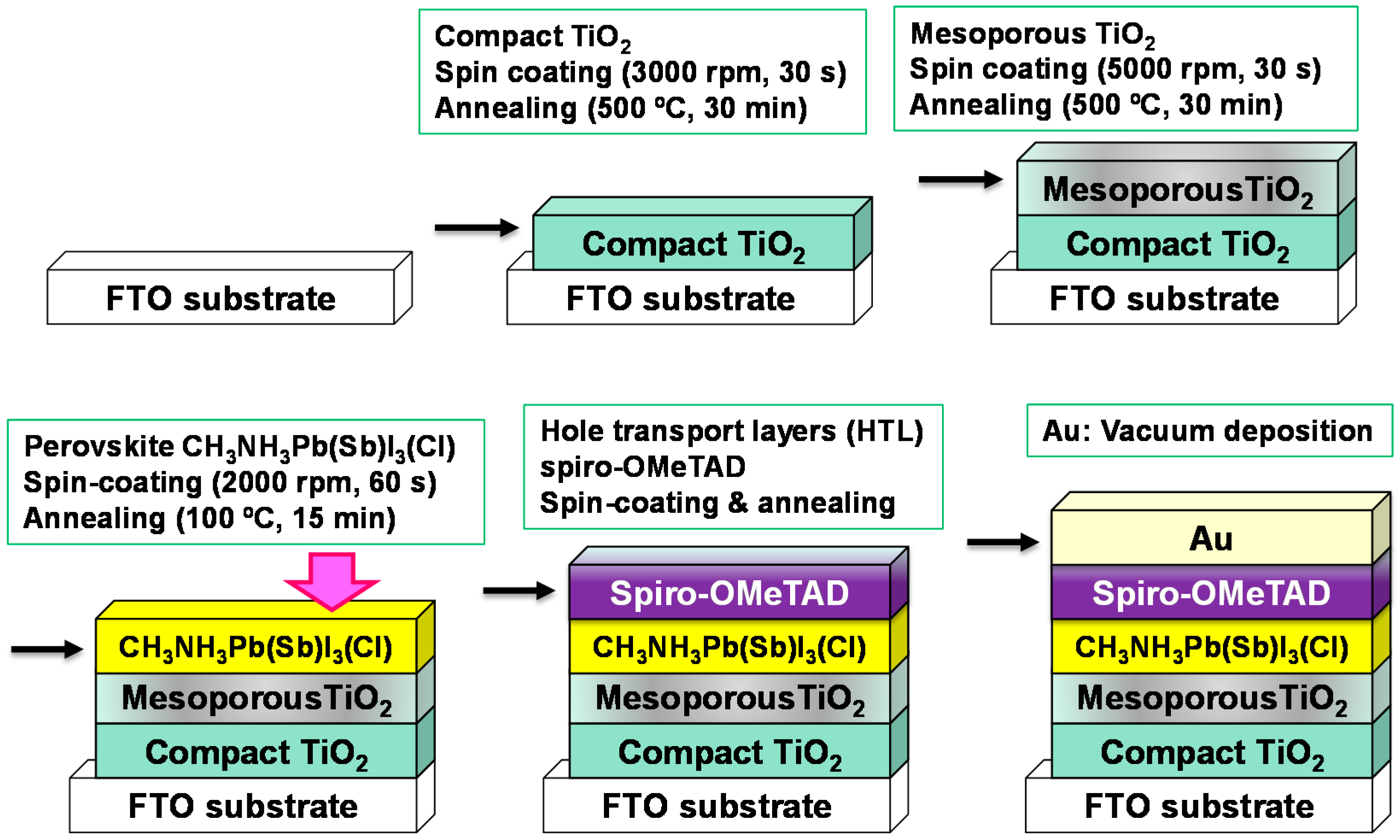
2. Materials and Methods

A schematic illustration for the fabrication of the present TiO2/CH3NH3Pb(Sb)I3(Cl) photovoltaic cells is shown in Figure 1. The details of the fabrication process are described in the reported papers [8,19,27,28,29,30], except for SbI3 [22]. F-doped tin oxide (FTO) substrates were cleaned using an ultrasonic bath with acetone and methanol, and dried under nitrogen gas. 0.15 M and 0.30 M TiO2 precursor solution was prepared from titanium diisopropoxide bis(acetylacetonate) (Sigma-Aldrich, Tokyo, Japan, 0.055 mL and 0.11 mL) with 1-butanol (1 mL), and the 0.15 M TiO2 precursor solution was spin-coated on the FTO substrate at 3000 rpm for 30 s, and annealed at 125 °C for 5 min. Then, the 0.30 M TiO2 precursor solution was spin-coated on the TiOx layer at 3000 rpm for 30 s, and annealed at 125 °C for 5 min. This process of 0.30 M solution was performed two times, and the FTO substrate was sintered at 500 °C for 30 min to form the compact TiO2 layer. After that, TiO2 paste was coated on the substrate by spin-coating at 5000 rpm for 30 s. For the mesoporous TiO2 layer, the TiO2 paste was prepared with TiO2 powder (Nippon Aerosil, Tokyo, Japan, P-25) with poly(ethylene glycol) (Nacalai Tesque, Kyoto, Japan, PEG #20000) in ultrapure water. The solution was mixed with acetylacetone (Wako Pure Chemical Industries, Osaka, Japan, 10 μL) and triton X-100 (Sigma-Aldrich, Tokyo, Japan, 5 μL) for 30 min, and was left for 12 h to suppress the bubbles in the solution. The cells were annealed at 120 °C for 5 min and at 500 °C for 30 min to form the mesoporous TiO2 layer [31,32]. For the preparation of the perovskite compounds, a solution of CH3NH3I (Showa Chemical Co., Ltd., Tokyo, Japan, 98.8 mg), PbI2 (Sigma-Aldrich, Tokyo, Japan), NH4Cl (Wako Pure Chemicals Industries, Ltd., Osaka, Japan), and SbI3 (Sigma-Aldrich), with a desired mole ratio in γ-butyrolactone (Nacalai Tesque, 275 μL), and N,N-dimethylformamide (DMF, Nacalai Tesque, 225 μL) was mixed at 60 °C. Addition of the DMF to γ-butyrolactone and NH4Cl to the perovskite phase would improve photovoltaic properties [25,26,33]. The detailed preparation compositions of TiO2/CH3NH3Pb(Sb)I3(Cl) cells with different additives are listed in Table 1. The solution of CH3NH3Pb(Sb)I3(Cl) was then introduced into the TiO2 mesopores by a spin-coating method and annealed at 100 °C for 15 min. Then, a hole transport layer (HTL) was prepared by spin-coating. As the HTL, a solution of 2,2',7,7'-tetrakis[N,Ndi(p-methoxyphenyl)amino]-9,9'-spirobifluorene (spiro-OMeTAD, Wako Pure Chemical Industries, 36.1 mg) in chlorobenzene (Wako Pure Chemical Industries, 0.5 mL) was mixed with a solution of lithium bis(trifluoromethylsulfonyl)imide (Li-TFSI, Tokyo Chemical Industry, Tokyo, Japan, 260 mg) in acetonitrile (Nacalai Tesque, 0.5 mL) for 12 h. The former solution with 4-tert-butylpyridine (Aldrich, 14.4 μL) was mixed with the Li-TFSI solution (8.8 μL) for 30 min at 70 °C. All procedures were carried out in ordinary air. Finally, gold (Au) metal contacts were evaporated as top electrodes. Layered structures of the present photovoltaic cells were denoted as FTO/TiO2/CH3NH3Pb(Sb)I3(Cl)/spiro-OMeTAD/Au, as shown in Figure 1.
The J-V characteristics of the photovoltaic cells were measured under illumination at 100 mW cm−2 by using an AM 1.5 solar simulator (San-ei Electric, Osaka, Japan, XES-301S). The solar cells were illuminated through the side of the FTO substrates, and the illuminated area was 0.090 cm2. The IPCE of the cells were also investigated (Enli Technology, Kaohsiung City, Taiwan, QE-R). The microstructures of the thin films were investigated by using an X-ray diffractometer (Bruker, Kanagawa, Japan, D2 PHASER), an optical microscope (Nikon, Tokyo, Japan, Eclipse E600) and a scanning electron microscope (Jeol, Tokyo, Japan, JSM-6010PLUS/LA) equipped with EDS.

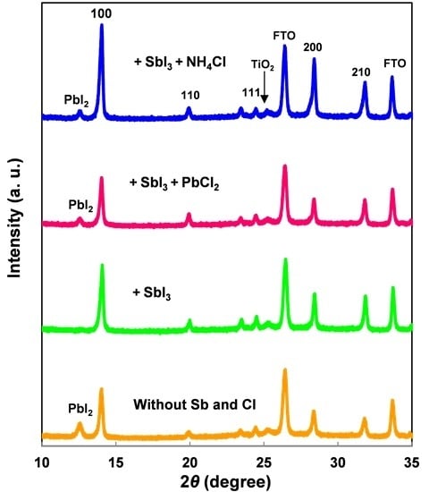
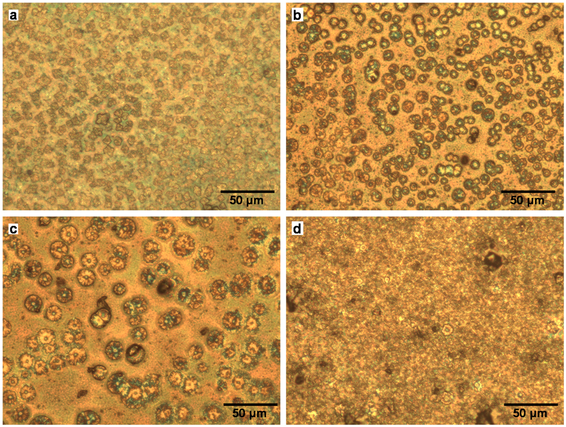
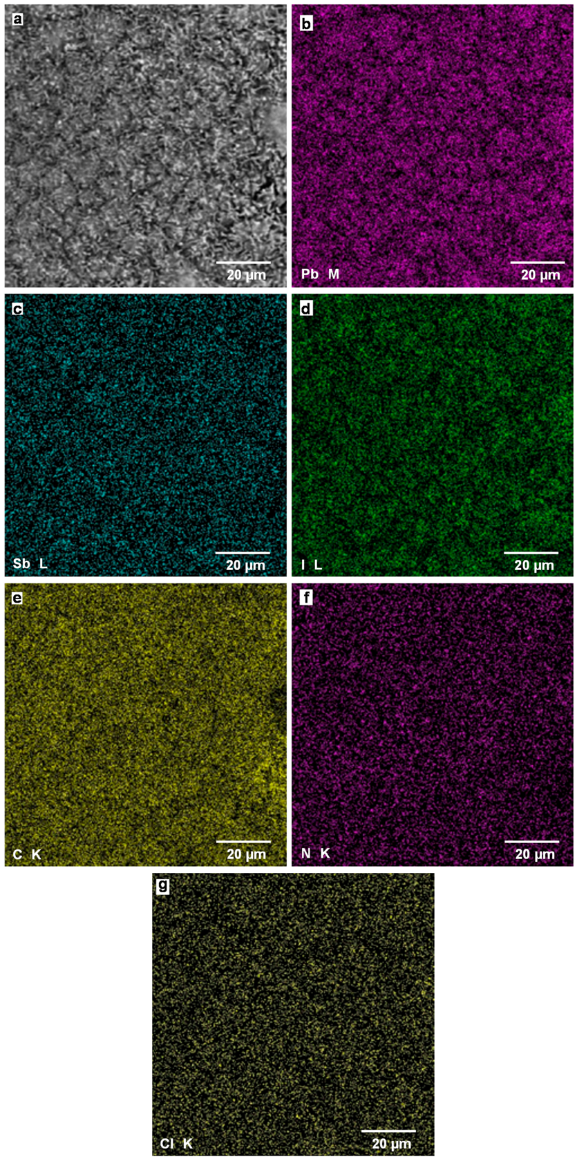
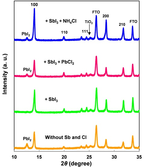
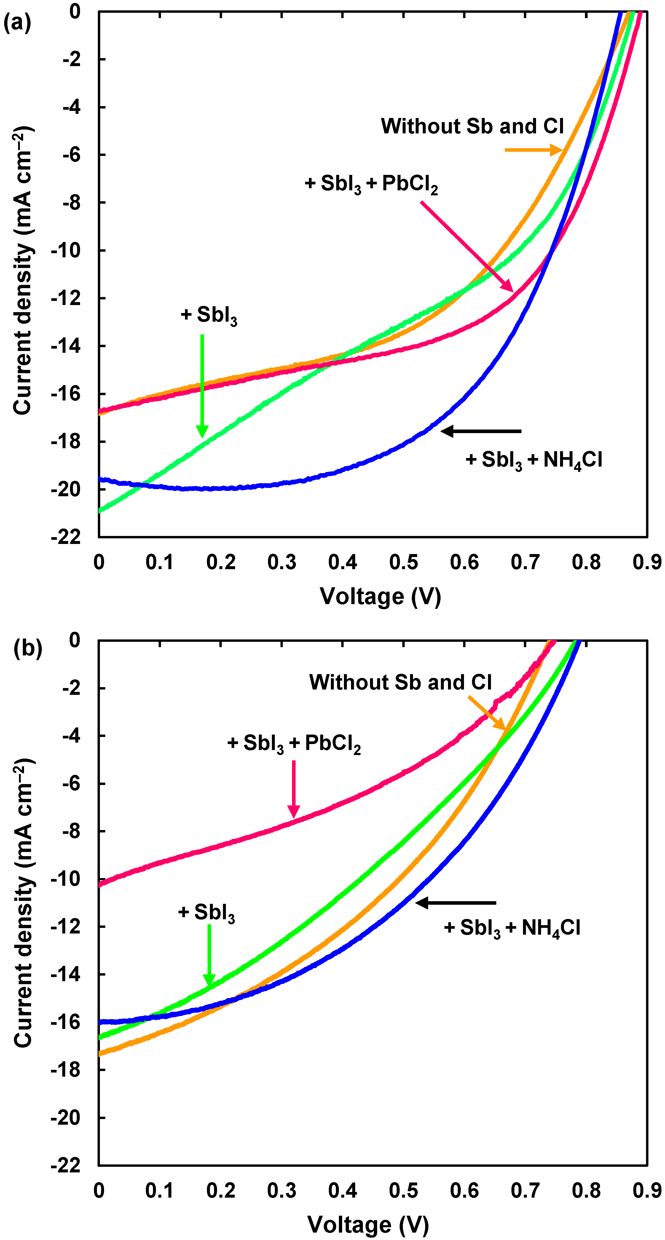
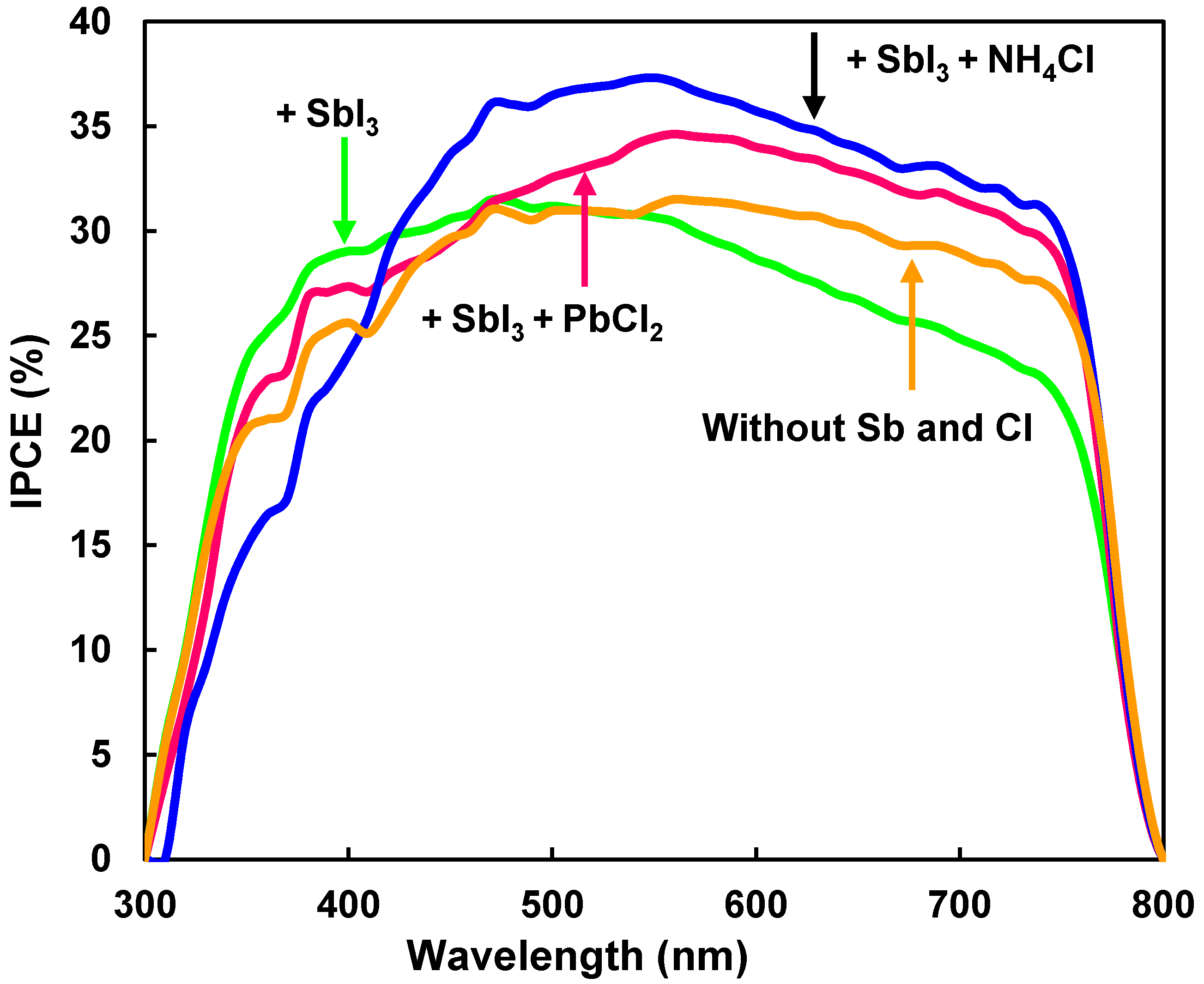
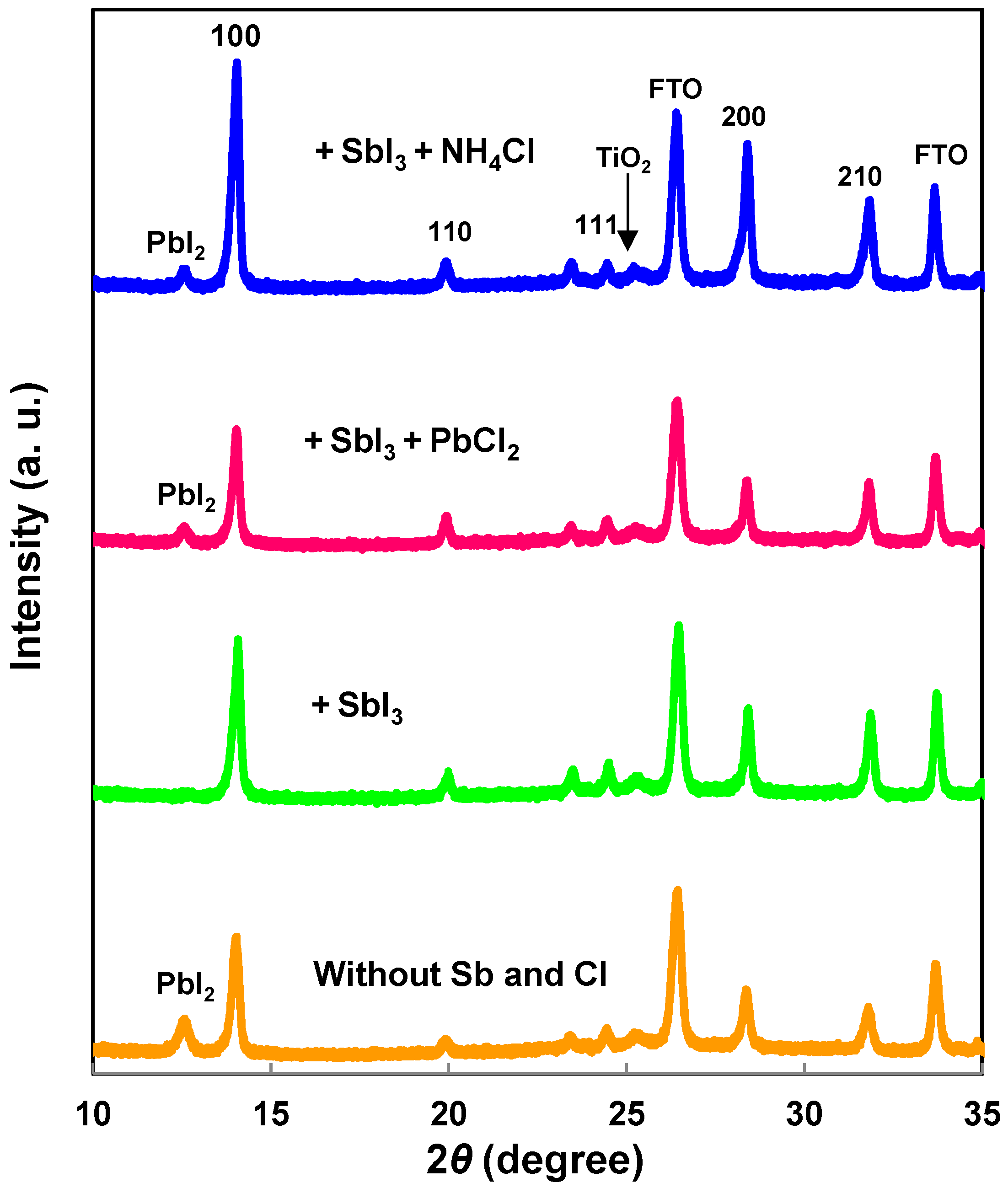
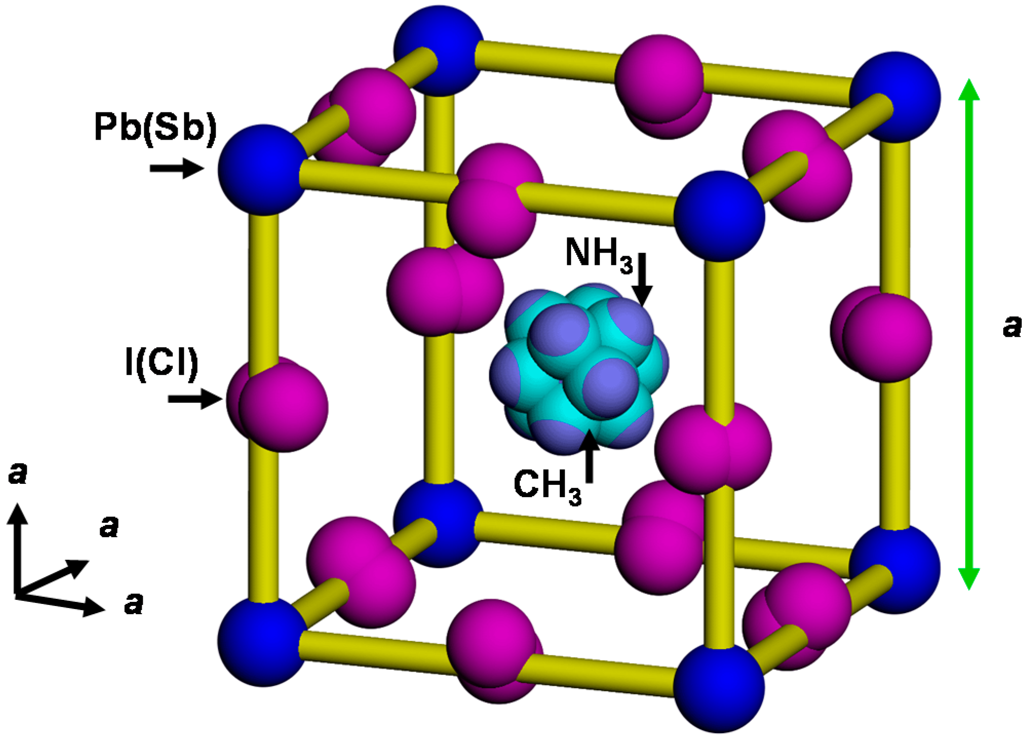
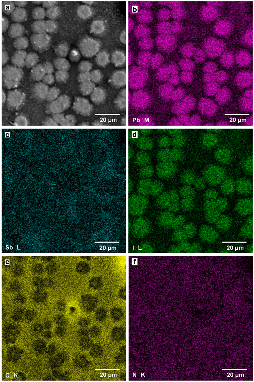
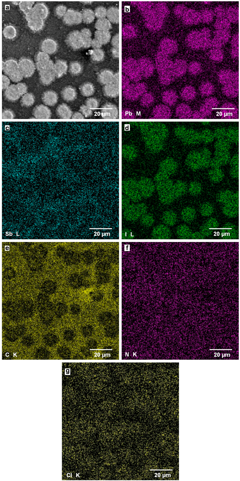
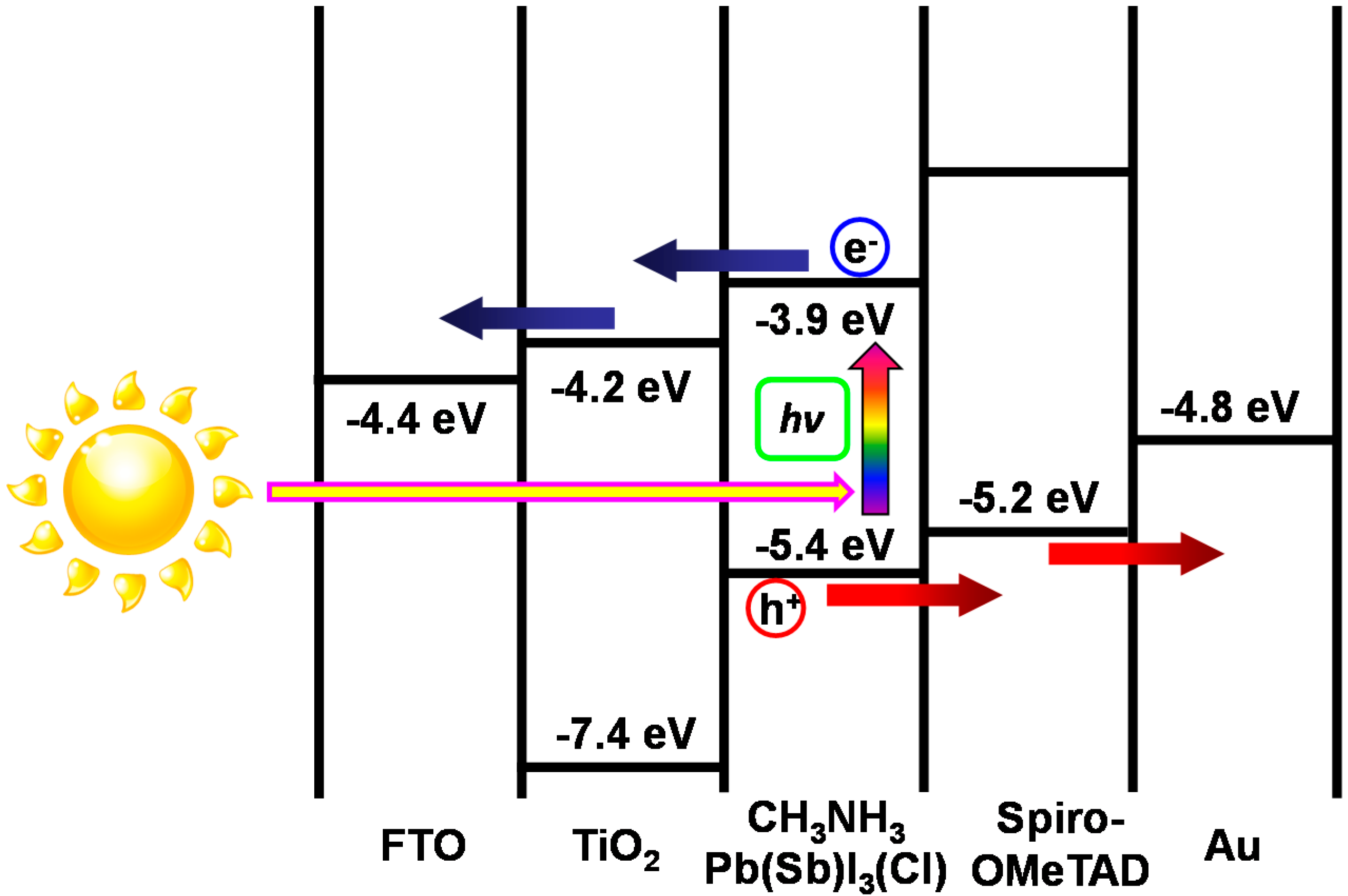
3. Results and Discussion

The J-V characteristics of the TiO2/CH3NH3Pb(Sb)I3(Cl)/spiro-OMeTAD photovoltaic cells under illumination are shown in Figure 2a, which indicates an effect of Sb and Cl addition to the CH3NH3PbI3. The measured photovoltaic parameters of TiO2/CH3NH3Pb(Sb)I3(Cl) cells are summarized in Table 2. The CH3NH3PbI3 cell provided a power conversion efficiency (η) of 7.05%, and the averaged efficiency (ηave) of three electrodes on the cells is 6.66%, as listed in Table 2. A short-circuit current density (JSC) increased up to 20.9 mA·cm−2 by an addition of SbI3, which would indicate an increase of carrier concentration. The highest efficiency was obtained for a cell added with SbI3 + NH4Cl, which provided an η of 9.71%, a fill factor (FF) of 0.579, a short-circuit current density (JSC) of 19.6 mA cm−2, and an open-circuit voltage (VOC) of 0.843 V. An increase of photocurrent for the (SbI3 + NH4Cl)-added sample is observed at ~0.2 V in Figure 2a. Since a small amount of carriers might be generated and charged in the TiO2 layer during J-V measurements under light irradiation and current flow, the electrical resistance would be reduced, and the photocurrent would increase. After 28 days, a decrease in the efficiencies of the cells were within 50%, except for the PbCl2 addition, as shown in Figure 2b and Table 2. Efficiency decay rates are also listed in Table 2, which indicates the NH4Cl additives would be effective for device stability. Although the JSC values were almost preserved after 28 days, the fill factors decreased. The black color of the perovskite phase became light brown after 28 days, which would indicate the degradation of the crystal structure of the perovskite phase.
IPCE spectra of the CH3NH3Pb(Sb)I3(Cl) cells are shown in Figure 3. The perovskite CH3NH3Pb(Sb)I3(Cl) shows photoconversion efficiencies between 300 nm and 800 nm, which almost agrees with reported energy gaps of 1.51 eV [34] and 1.61 eV [35] (corresponding to 821nm and 770 nm, respectively) for CH3NH3PbI3. The IPCE was improved in the range of 450–750 nm by adding a small amount of Sb and Cl. In the present work, the energy gaps of the CH3NH3Pb(Sb)I3(Cl) phase were almost constant of 1.55 eV even by the Sb- and Cl-doping, which corresponded well to the constant values of the open-circuit voltages.
XRD patterns of CH3NH3Pb(Sb)I3(Cl) cells on the FTO/TiO2 are shown in Figure 4. The diffraction peaks can be indexed by a cubic crystal system (Pm3m) for the CH3NH3Pb(Sb)I3(Cl) thin films. Although the deposited films are a single perovskite structure, broader diffraction peaks due to the PbI2 compound appeared in the CH3NH3Pb(Sb)I3(Cl) film, as shown in Figure 4. The Sb addition suppressed the formation of PbI2 [22].
The CH3NH3PbI3 crystals have perovskite structures, and both CH3NH3 ions and I ions are disordered, which results in the disordered cubic structure [22], as shown in Figure 5. For the as-deposited CH3NH3PbI3 thin film, only XRD peaks of CH3NH3PbI3 were observed, and no XRD peak of PbI2 was observed [27]. After annealing at 100 °C for 15 min, the unit cell volume decreased and an XRD peak of PbI2 appeared [27], which indicated partial separation of PbI2 from CH3NH3PbI3. The XRD result of CH3NH3PbI3 in Figure 4 also showed the existence of PbI2 after annealing at 100 °C for 15 min. This would indicate partial separation of PbI2 from CH3NH3PbI3 after annealing.
Optical microscope images of CH3NH3PbI3, CH3NH3Pb(Sb)I3(Cl) added with SbI3, SbI3 with PbCl2, and SbI3 with NH4Cl photovoltaic cells are shown in Figure 6a–d, respectively. Perovskite crystals with sizes of 5–10 μm are observed at the surface of the mesoporous TiO2, as shown in Figure 6a, and the crystals have a square-like shape. A completely different type of surface structure is observed for the CH3NH3Pb(Sb)I3(Cl) cells added with SbI3, as shown in Figure 6b. Perovskite crystals with sizes of ~10 μm are observed, and the crystals have a round shape, which would be an effect of SbI3 addition. The sizes of round-shaped crystals increased up to ~20 μm by an addition of SbI3 + PbCl2, as shown in Figure 6c. By adding SbI3 with NH4Cl to the CH3NH3PbI3, the surface morphology was drastically changed, as shown in Figure 6d, and few crystals with a special shape are observed. It is believed that these surface structures would affect the photovoltaic properties, in addition to the doping effect of Sb and Cl at the Pb and I sites, respectively.
Figure 7a is a SEM image of TiO2/CH3NH3Pb(Sb)I3(Cl) cell with an additive of SbI3, which corresponds to the OM image of Figure 6b. The particle sizes are ~10 μm, which agrees well with those observed in the OM image of Figure 6b. Elemental mapping images of Pb, Sb, I, C, and N by SEM-EDX are shown in Figure 7b–f, respectively. The elemental mapping images indicate the particles observed in Figure 7a correspond to the CH3NH3PbI3 phase. The composition ratio of metal elements Pb, Sb, I, and C:N were calculated from the EDX spectrum using background correction by normalizing the spectrum peaks on the atomic concentration, as listed in Table 3. This result indicates that I might be deficient from the starting composition of CH3NH3Pb(Sb)I3(Cl), and the deficient I might increase the hole concentration. In addition, carbon atoms are dispersed in the matrix, as shown in Figure 7e, which might be from γ-butyrolactone with a higher boiling point compared with that of DMF.
A SEM image of CH3NH3Pb(Sb)I3(Cl) cell with additives of SbI3 with PbCl2 is shown in Figure 8a. The particle sizes are 10–20 μm, which corresponds to those observed in the OM image of Figure 6c. Figure 8b–g are elemental mapping images of Pb M line, Sb L line, I L line, C K line, N K line, and Cl K line, respectively, which indicate the particles observed in Figure 8a correspond to the CH3NH3PbI3 phase. The composition ratio of metal elements and C:N were calculated from the EDX spectrum, as listed in Table 3, which indicates that I might be deficient from the starting composition of CH3NH3Pb(Sb)I3(Cl). In Figure 8e, carbon atoms are also dispersed in the matrix, which is similar to the observed image of Figure 7e.
Figure 9a is a SEM image of CH3NH3Pb(Sb)I3(Cl) cell with additives of SbI3 with NH4Cl. By adding SbI3 with NH4Cl to the CH3NH3PbI3, the surface morphology was drastically changed, and no special crystal shape is observed, which agrees well with the result of the OM image in Figure 6d. Elemental mapping images of Pb M line, Sb L line, I L line, C K line, N K line, and Cl K line are shown in Figure 9b–g, respectively. The images indicate the perovskite CH3NH3PbI3 phase is dispersed homogeneously on the photovoltaic device. The composition ratio of metal elements and C:N were calculated from the EDX spectrum, as listed in Table 3, which indicates that no major difference is observed compared with the other devices. This suggests that the homogeneous surface structures would improve the photovoltaic properties, in addition to the doping effect of Sb and Cl at the Pb and I sites, respectively. From the SEM-EDX result, site occupancies of I atom would also be less than 1, which might be due to the partial separation of PbI2 from the CH3NH3PbI3 phase.
Three assumed mechanisms could be considered for the increase of the photoconversion efficiencies. The first mechanism is as follows: I ions would be attracted at the I sites by Sb3+ with more ionic valence compared with that of Pb2+, which resulted in the suppression of PbI2 elimination from CH3NH3PbI3. The suppression of PbI2 would improve the TiO2/CH3NH3PbI3 interfacial structure, which also would improve the VOC values. As the amount of the Sb addition increase, the lattice constants would be decreased by an effect of Sb with a smaller ionic size compared with Pb.
The second mechanism is as follows: when a small amount of Cl was doped in the CH3NH3PbI3 phase, diffusion length of excitons would be lengthened by the doped Cl atoms [7,20], which would result in the increase of the JSC values.
The third is as follows: by adding SbI3 with NH4Cl to the CH3NH3PbI3, the homogeneous surface and interfacial structures formed, which improved the photovoltaic properties, especially the FF values. In addition, the doping effects of Sb and Cl at the Pb and I sites, respectively, would also contribute the improvement of the JSC values. Further studies are needed for precise structure determination of the perovskite structure.
Although the device performance may not be perfectly optimized, the reproducibility of efficiency increases by elemental doping, such as with Cl or Sb, were confirmed in the present and previously reported works [7,20,22,25]. Therefore, it is believed that the addition of dopants, such as Cl or Sb, to the perovskite phase would be effective for the development of device performance. The effect of the Cl-doping without Sb-doping was not investigated in the present work, and further studies are needed.
An energy level diagram of TiO2/CH3NH3Pb(Sb)I3(Cl) photovoltaic cells is summarized as shown in Figure 10. The electronic charge generation is caused by light irradiation from the FTO substrate side. The TiO2 layer receives the electrons from the CH3NH3Pb(Sb)I3(Cl) crystal, and the electrons are transported to the FTO. The holes are transported to an Au electrode through spiro-OMeTAD. In the present work, the samples were prepared in air, which may result in the reduction of the stability. Perovskite crystals with higher quality should be prepared in further works.

4. Conclusions

Effects of SbI3, PbCl2, and NH4Cl addition to perovskite CH3NH3PbI3 precursor solutions on photovoltaic properties were investigated. TiO2/CH3NH3Pb(Sb)I3(Cl)-based photovoltaic devices were fabricated, and the microstructures of the devices were investigated by XRD, OM, and SEM-EDS. J–V characteristics and IPCE were improved by a small amount of Sb- and Cl-doping. The structural analysis also indicated the formation of a homogeneous microstructure by SbI3 addition with NH4Cl, which improved the FF values and photoconversion efficiencies.

Acknowledgments

This work was partly supported by Satellite Cluster Program of the Japan Science and Technology Agency, and a Grant-in-Aid for Scientific Research (C) No. 25420760.

Author Contributions

Takeo Oku wrote the manuscript and summarized the project. Yuya Ohishi fabricated and characterized the solar cells, and summarized the results. Atsushi Suzuki and Yuzuru Miyazawa supported the project.

Conflicts of Interest

The authors declare no conflict of interest.

References

  1. Kojima, A.; Teshima, K.; Shirai, Y.; Miyasaka, T. Organometal halide perovskites as visible-light sensitizers for photovoltaic cells. J. Am. Chem. Soc. 2009, 131, 6050–6051. [Google Scholar] [CrossRef] [PubMed]
  2. Im, J.H.; Lee, C.R.; Lee, J.W.; Park, S.W.; Park, N.G. 6.5% efficient perovskite quantum-dot-sensitized solar cell. Nanoscale 2011, 3, 4088–4093. [Google Scholar] [CrossRef] [PubMed]
  3. Kim, H.S.; Lee, C.R.; Im, J.H.; Lee, K.B.; Moehl, T.; Marchioro, A.; Moon, S.J.; Yum, J.H.; Humphry-Baker, R.; Moser, J.E.; et al. Lead iodide perovskite sensitized all-solid-state submicron thin film mesoscopic solar cell with efficiency exceeding 9%. Sci. Rep. 2012, 2. [Google Scholar] [CrossRef] [PubMed]
  4. Grinberg, I.; West, D.V.; Torres, M.; Gou, G.; Stein, D.M.; Wu, L.; Chen, G.; Gallo, E.M.; Akbashev, A.; Davies, P.K.; et al. Perovskite oxides for visible-light-absorbing ferroelectric and photovoltaic materials. Nature 2013, 503, 509–512. [Google Scholar] [CrossRef] [PubMed]
  5. Lee, M.M.; Teuscher, J.; Miyasaka, T.; Murakami, T.N.; Snaith, H.J. Efficient hybrid solar cells based on meso-superstructured organometal halide perovskites. Science 2012, 338, 643–647. [Google Scholar] [CrossRef] [PubMed]
  6. Chung, I.; Lee, B.; He, J.Q.; Chang, R.P.H.; Kanatzidis, M.G. All-solid-state dye-sensitized solar cells with high efficiency. Nature 2012, 485, 486–489. [Google Scholar] [CrossRef] [PubMed]
  7. Stranks, S.D.; Eperon, G.E.; Grancini, G.; Menelaou, C.; Alcocer, M.J.P.; Leijtens, T.; Herz, L.M.; Petrozza, A.; Snaith, H.J. Electron-hole diffusion lengths exceeding 1 micrometer in an organometal trihalide perovskite absorber. Science 2013, 342, 341–344. [Google Scholar] [CrossRef] [PubMed]
  8. Burschka, J.; Pellet, N.; Moon, S.J.; Humphry-Baker, R.; Gao, P.; Nazeeruddin, M.K.; Grätzel, M. Sequential deposition as a route to high-performance perovskite-sensitized solar cells. Nature 2013, 499, 316–320. [Google Scholar] [CrossRef] [PubMed]
  9. Liu, M.; Johnston, M.B.; Snaith, H.J. Efficient planar heterojunction perovskite solar cells by vapour deposition. Nature 2013, 501, 395–398. [Google Scholar] [CrossRef] [PubMed]
  10. Liu, D.; Kelly, T.L. Perovskite solar cells with a planar heterojunction structure prepared using room-temperature solution processing techniques. Nat. Photonics 2014, 8, 133–138. [Google Scholar] [CrossRef]
  11. Wang, J.T.W.; Ball, J.M.; Barea, E.M.; Abate, A.; Alexander-Webber, J.A.; Huang, J.; Saliba, M.; Mora-Sero, I.; Bisquert, J.; Snaith, H.J.; et al. Low-temperature processed electron collection layers of graphene/TiO2 nanocomposites in thin film perovskite solar cells. Nano Lett. 2014, 14, 724–730. [Google Scholar] [CrossRef] [PubMed]
  12. Wojciechowski, K.; Saliba, M.; Leijtens, T.; Abate, A.; Snaith, H.J. Sub-150 °C processed meso-superstructured perovskite solar cells with enhanced efficiency. Energy Environ. Sci. 2014, 7, 1142–1147. [Google Scholar] [CrossRef]
  13. Zhou, H.; Chen, Q.; Li, G.; Luo, S.; Song, T.B.; Duan, H.S.; Hong, Z.; You, J.; Liu, Y.; Yang, Y. Interface engineering of highly efficient perovskite solar cells. Science 2014, 345, 542–546. [Google Scholar] [CrossRef] [PubMed]
  14. Jeon, N.J.; Noh, J.H.; Yang, W.S.; Kim, Y.C.; Ryu, S.; Seo, J.; Seok, S.I. Compositional engineering of perovskite materials for high-performance solar cells. Nature 2015, 517, 476–480. [Google Scholar] [CrossRef] [PubMed]
  15. Saliba, M.; Orlandi, S.; Matsui, T.; Aghazada, S.; Cavazzini, M.; Correa-Baena, J.P.; Gao, P.; Scopelliti, R.; Mosconi, E.; Dahmen, K.H.; et al. A molecularly engineered hole-transporting material for efficient perovskite solar cells. Nat. Energy 2016, 1, 15017. [Google Scholar] [CrossRef]
  16. Nie, W.; Tsai, H.; Asadpour, R.; Blancon, J.C.; Neukirch, A.J.; Gupta, G.; Crochet, J.J.; Chhowalla, M.; Tretiak, S.; Alam, M.A.; et al. High-efficiency solution-processed perovskite solar cells with millimeter-scale grains. Science 2015, 347, 522–525. [Google Scholar] [CrossRef] [PubMed]
  17. Miyasaka, T. Organo-lead halide perovskite: Rare functions in photovoltaics and optoelectronics. Chem. Lett. 2015, 44, 720–729. [Google Scholar] [CrossRef]
  18. Shi, D.; Adinolfi, V.; Comin, R.; Yuan, M.; Alarousu, E.; Buin, A.; Chen, Y.; Hoogland, S.; Rothenberger, A.; Katsiev, K.; et al. Low trap-state density and long carrier diffusion in organolead trihalide perovskite single crystals. Science 2015, 347, 519–522. [Google Scholar] [CrossRef] [PubMed]
  19. Oku, T.; Suzuki, K.; Suzuki, A. Effects of chlorine addition to perovskite-type CH3NH3PbI3 photovoltaic devices. J. Ceram. Soc. Jpn. 2016, 124, 234–238. [Google Scholar] [CrossRef]
  20. Dong, Q.; Fang, Y.; Shao, Y.; Mulligan, P.; Qiu, J.; Cao, L.; Huang, J. Electron-hole diffusion lengths > 175 μm in solution-grown CH3NH3PbI3 single crystals. Science 2015, 347, 967–970. [Google Scholar] [CrossRef] [PubMed]
  21. Hao, F.; Stoumpos, C.C.; Cao, D.H.; Chang, R.P.; Kanatzidis, M.G. Lead-free solid-state organic-inorganic halide perovskite solar cells. Nat. Photonics 2014, 8, 489–494. [Google Scholar] [CrossRef]
  22. Oku, T.; Ohishi, Y.; Suzuki, A. Effects of antimony addition to perovskite-type CH3NH3PbI3 photovoltaic devices. Chem. Lett. 2016, 45, 134–136. [Google Scholar] [CrossRef]
  23. Krishnamoorthy, T.; Ding, H.; Yan, C.; Leong, W.L.; Baikie, T.; Zhang, Z.; Sherburne, M.; Li, S.; Asta, M.; Mathews, N.; et al. Lead-free germanium iodide perovskite materials for photovoltaic applications. J. Mater. Chem. A 2015, 3, 23829–23832. [Google Scholar] [CrossRef]
  24. Ohishi, Y.; Oku, T.; Suzuki, A. Fabrication and characterization of perovskite-based CH3NH3Pb1-xGexI3, CH3NH3Pb1-xTlxI3 and CH3NH3Pb1-xInxI3 photovoltaic devices. AIP Conf. Proc. 2016, 1709. [Google Scholar] [CrossRef]
  25. Zuo, C.; Ding, L. An 80.11% FF record achieved for perovskite solar cells by using the NH4Cl additive. Nanoscale 2014, 6, 9935–9938. [Google Scholar] [CrossRef] [PubMed]
  26. He, J.; Chen, T. Additive regulated crystallization and film formation of CH3NH3PbI3−xBrx for highly efficient planar-heterojunction solar cells. J. Mater. Chem. A 2015, 3, 18514–18520. [Google Scholar] [CrossRef]
  27. Oku, T.; Zushi, M.; Imanishi, Y.; Suzuki, A.; Suzuki, K. Microstructures and photovoltaic properties of perovskite-type CH3NH3PbI3 compounds. Appl. Phys. Express 2014, 7. [Google Scholar] [CrossRef]
  28. Oku, T.; Iwata, T.; Suzuki, A. Effects of niobium addition into TiO2 layers on CH3NH3PbI3-based photovoltaic devices. Chem. Lett. 2015, 44, 1033–1035. [Google Scholar] [CrossRef]
  29. Zushi, M.; Suzuki, A.; Akiyama, T.; Oku, T. Fabrication and characterization of TiO2/CH3NH3PbI3-based photovoltaic devices. Chem. Lett. 2014, 43, 916–918. [Google Scholar] [CrossRef]
  30. Oku, T.; Matsumoto, T.; Suzuki, K.; Suzuki, A. Fabrication and characterization of a perovskite-type solar cell with a substrate size of 70 mm. Coatings 2015, 5, 646–655. [Google Scholar] [CrossRef]
  31. Oku, T.; Kakuta, N.; Kobayashi, K.; Suzuki, A.; Kikuchi, K. Fabrication and characterization of TiO2-based dye-sensitized solar cells. Prog. Nat. Sci. 2011, 21, 122–126. [Google Scholar] [CrossRef]
  32. Kanayama, M.; Oku, T.; Suzuki, A.; Yamada, M.; Sakamoto, H.; Minami, S.; Kohno, K. Low temperature fabrication of perovskite solar cells with TiO2 nanoparticle layers. AIP Conf. Proc. 2015, 1709. [Google Scholar] [CrossRef]
  33. Kim, H.B.; Choi, H.; Jeong, J.; Kim, S.; Walker, B.; Song, S.; Kim, J.Y. Mixed solvents for the optimization of morphology in solution-processed, inverted-type perovskite/fullerene hybrid solar cells. Nanoscale 2014, 6, 6679–6683. [Google Scholar] [CrossRef] [PubMed]
  34. Baikie, T.; Fang, Y.; Kadro, J.M.; Schreyer, M.; Wei, F.; Mhaisalkar, S.G.; Gräetzel, M.; White, T.J. Synthesis and crystal chemistry of the hybrid perovskite (CH3NH3)PbI3 for solid-state sensitised solar cell applications. J. Mater. Chem. A 2013, 1, 5628–5641. [Google Scholar] [CrossRef]
  35. Yamada, Y.; Nakamura, T.; Endo, M.; Wakamiya, A.; Kanemitsu, Y. Near-band-edge optical responses of solution-processed organic-inorganic hybrid perovskite CH3NH3PbI3 on mesoporous TiO2 electrodes. Appl. Phys. Express 2014, 7. [Google Scholar] [CrossRef]
Figure 1. Schematic illustration for the fabrication of CH3NH3Pb1-xSbxI3-yCly photovoltaic cells.
Metals 06 00147 g001
Figure 2. (a) J-V characteristic of CH3NH3Pb(Sb)I3(Cl) photovoltaic cells; (b) J-V characteristic after 28 days.
Metals 06 00147 g002
Figure 3. IPCE (incident photon-to-current conversion efficiency) spectra of CH3NH3Pb(Sb)I3(Cl) cells.
Metals 06 00147 g003
Figure 4. XRD patterns of CH3NH3Pb(Sb)I3(Cl) cells.
Metals 06 00147 g004
Figure 5. Structure model of cubic CH3NH3Pb(Sb)I3(Cl).
Metals 06 00147 g005
Figure 6. Optical microscope images of CH3NH3Pb(Sb)I3(Cl) cells; The additives are (a) none; (b) SbI3; (c) SbI3 with PbCl2; and (d) SbI3 with NH4Cl, respectively.
Metals 06 00147 g006
Figure 7. (a) SEM image of CH3NH3Pb(Sb)I3(Cl) cell with an additive of SbI3; Elemental mapping images of (b) Pb M line, (c) Sb L line, (d) I L line, (e) C K line, and (f) N K line.
Metals 06 00147 g007
Figure 8. (a) SEM image of CH3NH3Pb(Sb)I3(Cl) cell with additives of SbI3 with PbCl2; Elemental mapping images of (b) Pb M line, (c) Sb L line, (d) I L line, (e) C K line, (f) N K line, and (g) Cl K line.
Metals 06 00147 g008
Figure 9. (a) SEM image of CH3NH3Pb(Sb)I3(Cl) cell with additives of SbI3 with NH4Cl; Elemental mapping images of (b) Pb M line, (c) Sb L line, (d) I L line, (e) C K line, (f) N K line, and (g) Cl K line.
Metals 06 00147 g009
Figure 10. Energy level diagram of CH3NH3Pb(Sb)I3(Cl) cells.
Metals 06 00147 g010
Table 1. Preparation composition of TiO2/CH3NH3Pb1-xSbxI3Cl3-y cells with different additives.
Preparation CompositionAmount of Additives
CH3NH3PbI3None
CH3NH3Pb0.97Sb0.03I3.03SbI3 (9.5 mg)
CH3NH3Pb0.93Sb0.03I2.99Cl0.04SbI3 (9.5 mg) + PbCl2 (7 mg)
CH3NH3Pb0.97Sb0.03I3.03Cl0.30SbI3 (9.5 mg) + NH4Cl (10 mg)
Table 2. Measured photovoltaic parameters (average and top) of TiO2/CH3NH3Pb(Sb)I3(Cl) cells.
AdditiveJSC (mA·cm−2)VOC (V)FFH (%)ηave (%)Decay Rate (%/Week)
None16.80.8700.4827.056.66-
SbI320.90.8770.3867.086.57-
SbI3 + PbCl216.70.8880.5518.177.51-
SbI3 + NH4Cl19.60.8560.5799.719.02-
After 28 days------
None17.30.7390.3904.984.567.88
SbI316.60.7820.3324.314.029.70
SbI3 + PbCl213.10.5700.4023.002.8515.5
SbI3 + NH4Cl16.00.7870.4385.514.9911.2
Table 3. Measured compositions of TiO2/CH3NH3Pb(Sb)I3(Cl) cells. BDL means below detection limit.
AdditivePb (%)Sb (%)I (%)Cl (%)C:N
SbI333.7BDL66.3-60.5:39.5
SbI3 + PbCl230.5BDL67.52.058.4:41.6
SbI3 + NH4Cl31.30.267.31.261.3:38.7

