Abstract
Some characteristic features of band structures, like the band degeneracy at high symmetry points or the existence of energy gaps, usually reflect the symmetry of the crystal or, more precisely, the symmetry of the wave vector group at the relevant points of the Brillouin zone. In this paper, we will illustrate this property by considering two-dimensional (2D)-hexagonal lattices characterized by a possible two-fold degenerate band at the K points with a linear dispersion (Dirac points). By combining scanning tunneling spectroscopy and angle-resolved photoemission, we study the electronic properties of a similar system: the Ag/Cu(111) interface reconstruction characterized by a hexagonal superlattice, and we show that the gap opening at the K points of the Brillouin zone of the reconstructed cell is due to the symmetry breaking of the wave vector group.
1. Introduction
Symmetry is probably one of the most general and fundamental concepts in physics, and its central role was only recognized in the 20th century. The most emblematic example is particle physics, for which the space-time symmetry and the internal symmetries are essential to understand the interactions among elementary particles. The fundamental equations of physics, like Maxwell or Dirac equations, can be considered as a direct consequence of the symmetry principles. Group theory is then a powerful tool to exploit the symmetry concepts in all domains of physics. As an example, the representation theory shows that the essential degeneracy of an energy level is given by the dimension of the corresponding irreducible representation of the symmetry group.
Moreover, symmetry breaking emerged more recently and was shown to be a generic behavior in matter. In his famous article “More is different”, Anderson, P.W. discussed the broken symmetry and the nature of the hierarchical structure of science [1]. He showed that for large systems, the physical states are usually less symmetrical than the laws. A trivial example is crystals, which clearly violate the homogeneity and isotropy of space and physical laws. Such a behavior is an example of the spontaneous symmetry breaking mechanism. More elaborate is the Higgs mechanism and the generation of mass for bosons in particle physics [2]. Such a mechanism is also useful in condensed matter physics, in particular, for phase transitions [3]. Another kind of symmetry breaking can be defined: intrinsic broken symmetry corresponding to the modification of the symmetry of the Hamiltonian. As an example, an external magnetic field yields the breaking of time reversal symmetry (Zeeman effect); it slightly affects the energy spectra of atoms, but usually changes the degeneracy. In the following, we will discuss this kind of symmetry breaking, yielding the modification of electronic properties at the surface of a crystal.
In this paper, we study the interplay between symmetry and the electronic properties of 2D systems with hexagonal periodic arrangements. Such honeycomb lattices can exhibit, in the most symmetrical case, singular electronic properties, which are associated with crossing bands at the K points of the Brillouin zone (BZ) with linear dispersions. When this band crossing occurs at the Fermi energy, the low energy excitations can be described by an effective 2D Dirac equation of massless fermions, like in graphene [4]. This singular behavior is directly related to the symmetry of the wave vector group at the K points and to the dimension of the corresponding irreducible representation [5]. A symmetry breaking with a change of the wave vector group can lead to non-crossing bands and, then, to gap opening and curvature of the band dispersion. This was observed, for example, by growing a graphene layer on a crystal surface [6]. The broken symmetry is then reflected by a generation of mass, since the Dirac equation governing the low energy excitations corresponds to finite mass associated with the gap width. The system we studied in this paper, the reconstructed Ag/Cu(111) surface, exhibits this kind of symmetry. Due to the misfit of lattice parameters of Ag and Cu, one monolayer of Ag epitaxially grown on Cu(111) induces a reconstruction consisting of an hexagonal lattice of dislocation loops [7]. In the (111) surface of noble metals, the surface states exhibit a nearly free electron-like behavior (Shockley states), and in Ag/Cu(111), its band structure is characterized by gaps at the boundary of the reconstructed Brillouin zone. Band gap opening reflects the symmetry of wave vector groups, and we show that the gap magnitudes can be used to obtain the surface potential or at least their first Fourier components. After a general discussion of the symmetry on the hexagonal 2D lattices and, in particular, the relation between the gap at the K point and the group of the wave vector, we present angle-resolved photoemission spectroscopy (ARPES) and scanning tunneling microscopy and spectroscopy (STM/STS) results obtained on Ag/Cu(111) and K/Ag/Cu(111). For these interfaces, minigaps appear at the K points of the surface Brillouin zone. We discuss, in detail, this system, especially the relation between symmetry and the surface potential.
2. Experimental Details and Method of Calculations
2.1. Experimental Details
The angle-resolved photoemission experiments were performed at 80 K with a Scienta 200 high-resolution hemispherical analyzer using photon energy of hν = 21.2 eV. The presented ARPES maps correspond to second derivative signals in order to emphasize the energy gaps. Data points in Figure 3 and Figure 4 are obtained from standard line fits of individual energy distribution curves (EDCs), using Lorentzian functions and Fermi edge functions. STM and STS experiments have been carried out using Low Temperature-Omicron STM. The spectra and maps were recorded at 5 K in the open feedback loop mode using the lock-in technique with a bias modulation of 5 mV at 2300 Hz (stabilization parameters: tunneling current 1 nA, bias voltage 1.0 V). Before transferring to the STM cryostat at 5 K, the Ag monolayer is evaporated at 400 K on the clean Cu(111) crystal. This process leads to the sharp ∼(9.5 × 9.5) hexagonal lattice of triangular dislocations. Evaporation of K atoms on the Ag/Cu(111) surface at room temperature was achieved by heating a standard K getter.
2.2. Calculation Method
Calculations of the electronic properties of the Shockley states are carried out by a direct diagonalization of the Schrödinger equation with a potential defined by the first Fourier components we experimentally deduced from the gap widths. As Shockley states exhibit nearly free electron-like behavior, a plane wave basis is appropriate, and we limit to the first 36 waves around the Γ point. Additional plane waves have negligible effects. Local Density of states (LDOS) maps and spectra are obtained resolving the Hamiltonian for more than 1500 wave vectors in the first Brillouin zone (BZ) and by taking into account a 15 meV Gaussian energy broadening.
3. Results and Discussion
3.1. Symmetry Analysis
Let us consider a 2D hexagonal lattice. The unit cell is diamond-shaped but, the Wigner–Seitz cell is hexagonal. The Brillouin zone, which is only related to translational periodicity, is also hexagonal, but rotated by with respect to the Wigner–Seitz cell, and the symmetry elements of direct and reciprocal space are the same. We will consider the two high symmetry M and K points. We have three inequivalent (not related by a reciprocal space vector) M points (M, , ) and two inequivalent K points (K, ), as shown in Figure 1a. We would like to point out the peculiar property of the K point with respect to time reversal symmetry. By contrast to the M point, time reversal symmetry couples the two non-equivalent K and points. Let us choose the 2D highly symmetric group, or . This is the 2D-space group of graphene. Among the symmetry elements, one has two families of three-fold mirrors, and , as illustrated in Figure 1b, one () crossing all M points, the other one () all K points. For the electronic band structure, we have to consider the group of the wave vector at the high symmetry points of the BZ. The wave vector group is the group of transformations conserving the wave vector in the first Brillouin zone (i.e., modulo a reciprocal space vector). At the Γ point, the symmetry group of the wave vector is ; at the M point it is , and at the K point it is . These considerations are important for the essential band degeneracy, since the band energy levels at a given wave vector of the first Brillouin zone are associated with the irreducible representations of these groups. As an example, the K point wave vector group is non-abelian with a two-dimensional irreducible representation, E, corresponding to a two-fold degenerate band. This is the case of the -derived bands of graphene, which exhibit the famous Dirac points characterized by the crossing of two linear dispersive bands at the K points [4]:
where is the crystal momentum with respect to the K point and the Fermi velocity.
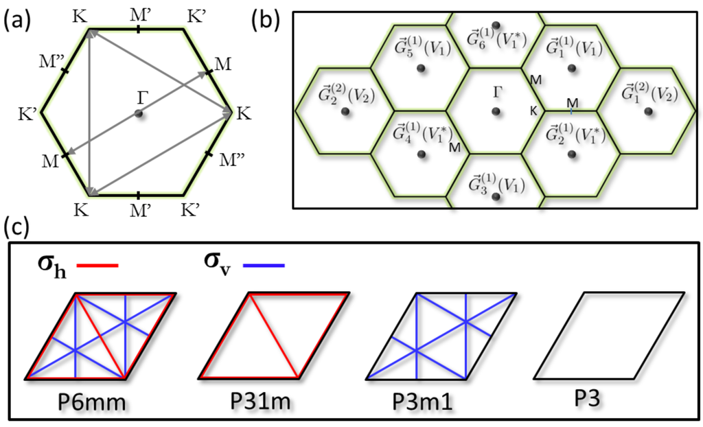
Figure 1.
(a) The first Brillouin zone of a reciprocal space of 2D hexagonal lattices. The different M and K points are indicated (equivalent points are connected by a reciprocal space vector); (b) The unit cell with the symmetry mirrors for , , and space groups; (c) The reciprocal vectors in the first () and second () rings around Γ, as well as the corresponding Fourier component of the potential (see text).
Let us consider the breakdown of this symmetry by removing one of the mirror families. The removal of the family leads to the (or ) space group. The consequence is a change of the wave vector groups; at Γ, it is now or , at M, or m, and at K, or three. As the K-vector group is now abelian, the essential degeneracy is left (the 2D-irreducible representation, E, of is decomposed in two 1D-representations of ), and one expects the band gap opening with the disappearance of the linear dispersion. Therefore, the Dirac points characterized by massless fermions for disappear, and the symmetry breaking leads to massive fermions and, then, to a gap. The dispersion relation close to the K points can be written:
where is the mass term and the gap width. This is what happens in the hexagonal boron nitride layer or epitaxial graphene, for example, on Ir(111) [8]. We will discuss in the following the triangular reconstruction of Ag/Cu(111), which exhibits this peculiar symmetry, and we will investigate the consequences on the Shockley surface state properties.
If the other mirror family () is removed, the situation is completely different. The space group is then (or ), and the wave vector groups are at Γ and at M, but remain at K. Therefore, no change is expected in the band degeneracy, and the band states corresponding to the two-dimensional E irreducible representation remain massless (linear dispersion with no gap), like in the high symmetry group. This behavior shows that the pertinent symmetry breaking is related to the symmetry of the wave vector group. For the lowest symmetric group, both mirror families are removed, leading to the opening of a gap at K points.
3.2. The Ag/Cu(111) Reconstruction
As discussed above, the (111) surfaces of noble metals are known to exhibit surface states with a nearly free electron-like behavior (Shockley surface states [9]). Due to their surface localization, these Shockley bands are very sensitive to any surface modification. Deposition of atoms and formation of an ultra-thin epitaxial layer yield a change of the surface state energy and/or effective mass. For example, one monolayer of Ag epitaxially grown on Cu(111) leads to an energy shift of the surface state, but also to a reconstruction, due to the different atomic radius of Cu and Ag. As a consequence, a super-periodic cell ∼(9.5 × 9.5) is observed, characterized by an hexagonal array of triangular dislocations [7,10]. The surface Brillouin zone of the reconstructed layer is small, and the parabolic dispersions of the Shockley state exhibit deviations close to the zone boundaries with the gap opening [11,12,13]. These gaps result from the Bragg mechanism at these high symmetry points and lines. For example, the M point of the first Brillouin zone is situated between the Γ point and one reciprocal vector, (Figure 1b). In the nearly free electron framework, the band states at M are simply linear combinations of the incoming state, , and the diffracted one, (in the first approximation). The energy difference between these two band states ( is , where is the Fourier component of the surface potential, like in a simple 1D nearly-free-electron gas, discussed in solid state textbooks [14]. At the K point, the situation is more complicated. The K point is at the center of an equilateral triangle defined by Γ, and , and three states composed from , and are involved.
The widths of the gaps in the surface band structure give partial information about the potential associated with the reconstruction, but only occupied bands are accessible with ARPES, limiting the number of observable gaps. However, it has been shown that, by depositing K atoms, it is possible to shift the energy of the surface Shockley band towards higher binding energies [15,16]. We used this property in order to tune the energy gaps below the Fermi energy. These experimental gap widths allow one to determine several Fourier components and, then, to deduce the surface potential [17].
3.3. Symmetry and Potential Properties
We would like to discuss the link between the symmetry of the surface and the properties of the Fourier components of the potential, at least the first two ones. Firstly, we would like to consider the highly symmetric case corresponding to the space group. The presence of the six-fold axis induces that the Fourier components corresponding to the first six equivalent reciprocal vectors are all identical. In particular, one has:
Moreover, it is possible to show that this component is purely real. Indeed, time reversal symmetry (T), which, for a spinless particle, is simply the complex conjugate operator, transforms the potential according to:
since the potential is real. Then, one deduces that:
which proves with Equation (3) that the Fourier components, , are real. A typical band structure in the nearly free electron model is reported in Figure 2a (center panel). We also show the mirror symmetries in the Brillouin zone and the potential used to compute the band structure. This potential was obtained from the Fourier components associated with the reciprocal vectors in the first two rings around Γ, as illustrated in Figure 1b. The dispersions exhibit a first gap at M and linear dispersive crossing bands at the K point. This illustrates the symmetry origin of this singular behavior, since it is encountered both in graphene (tight binding bands) and in Ag/Cu(111) (nearly free electron bands).
When we remove one mirror family, either or , two kinds of reciprocal vectors appear in the first ring around Γ: three equivalent ones associated with , the three equivalent other ones being associated with (Figure 1b). For the space group (Figure 2b), the remaining mirrors () are along the directions and contain the six first reciprocal vectors in the second ring (, ). Therefore, this mirror symmetry does not couple the two kinds of reciprocal vectors of this ring, and the corresponding Fourier components of the potential can be complex (, and , ). On the other hand, the mirror couples the two sets of reciprocal vectors in the first ring (). Then, the first components (associated with the six reciprocal vectors of the first ring) are purely real: . The contrary behavior occurs for the space group (Figure 2c). The remaining mirrors () are along the directions and contain the six first reciprocal vectors in the first ring and couple the two kinds of reciprocal vectors in the second ring. As a consequence, the Fourier components of the second ring are purely real , whereas the components belonging to the first ring can be complex. The band structure of Figure 2b illustrates the consequence on the electronic properties. As discussed above, the wave vector group at K remains for , and no gap opens; whereas it is only for , and a gap appears with curvature in the band dispersion. Finally, if the two families of mirrors are removed (Figure 2d and the space group), the first components (first ring) and the second ones (second ring) are both complex, the K-wave vector is and a gap is also exhibited at the K points.
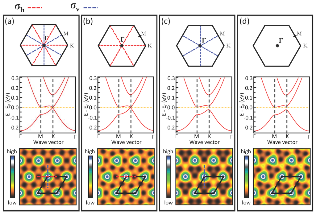
Figure 2.
Brillouin zone with the mirror symmetries (top panel), schematic band structures in the nearly free electron model (center panel) and the corresponding direct space surface potential (bottom panel) for the different space groups: (a) ; (b) ; (c) ; and (d) . Comparison between these band structures shows that the mirrors are necessary to have a gapless Dirac point at K.
This symmetry analysis shows that the opening of a gap at the K point associated with massive fermions is simply related to the wave vector group at this high symmetry point. In the nearly free electron approach valid for Shockley surface states of a (111) noble metal surface, the symmetry imposes some rules for the Fourier components, in particular, the value of the imaginary parts of these components.
3.4. Electronic Properties of Ag/Cu(111)
Figure 3a shows an STM image of the Ag/Cu(111) surface. It exhibits the triangular lattice of dislocation loops, evidencing that only the mirrors are symmetry elements, leading to a space group for this 2D crystal. Figure 3b reports the ARPES dispersion (the second derivative of the experimental signal) in the and directions for the Ag/Cu(111) surface and a K-doped surface. By doping the surface with K, it is possible to tune the surface state energy and, then, to measure the second energy gap at the M point, which is above the Fermi energy for the undoped surface. For the bare Ag/Cu(111) surface, a 80 meV gap is evidenced just below , whereas the change in curvature suggests that a gap could exist at at the K point. This is corroborated by the results on the K-doped surface, which indicates the gap opening at K and a third band dispersing upward (close up of Figure 3b). Moreover, inspection of the reciprocal space (Figure 1a) shows that the Γ, the K of the first Brillouin zone and the M point in the second zone are aligned. Therefore, the experimental dispersion along the direction allows one to probe the first gap at K and the second gap at M. This is exactly what is measured in the experimental spectra of the K-doped surface (Figure 3b). From the gap widths, it is possible to estimate the Fourier components of the surface potential. Indeed, due to the nearly free electron behavior of the Shockley states, only a few plane waves are involved in the high symmetry points, mainly two for M points and three for K points. As a consequence, in a first approximation, the gaps at M and K only depend on the first Fourier component, since it is straightforward to show that:
leading to a determination of the real and imaginary parts of the component. We find meV. The second component meV (purely real; see above) can be deduced for the gap appearing close to the Fermi energy for the doped surface at the M point. We would like to point out that, as the gap width is proportional to the imaginary part of , a purely real Fourier component leads to a zero gap at K, corroborating our discussion above based on symmetry arguments.
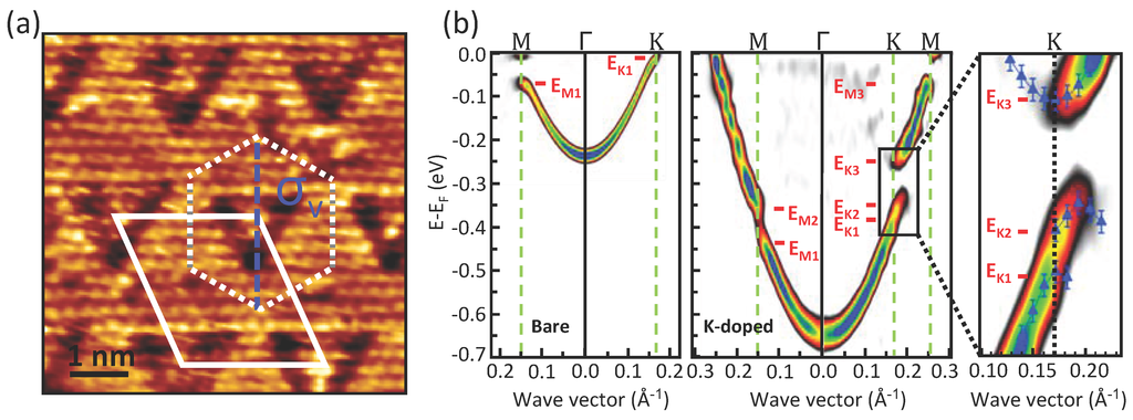
Figure 3.
(a) Scanning tunneling microscopy (STM) image of the Ag/Cu(111) surface with the unit cell and the three-fold mirror. Solid and dotted lines represent the unit and Wigner–Seitz cells, respectively; (b) Second derivative angle-resolved photoemission spectroscopy (ARPES) signal representing the band dispersions measured on Ag/Cu(111) (left) and a K-doped surface (closeup illustrating the three bands close to the K point).
The value is corroborated by the intensity of the folded band. Indeed, although the band dispersions are periodic in the reciprocal space, the spectral weight is not periodic, and the folded band intensity in the second Brillouin zone is a function of the Fourier component [18] and can be simply calculated. Figure 4a shows the experimental intensity in the direction for the main band and its replicate for the undoped surface. We also show the calculated ARPES intensity with experimentally deduced from the gaps. A very good agreement between experimental and calculated spectral intensities is obtained. With the and components we deduce from the gap widths at M and K, we can rebuild the potential associated with the Ag/Cu(111) reconstructed surface, as shown in Figure 4b. By solving numerically the Schrödinger equation with this potential, it is possible to compute the band structure in the high symmetry directions. The results are reported in Figure 4c and compared with the ARPES data (for the occupied states) and the density of states (occupied and unoccupied states) measured by scanning tunneling spectroscopy. A satisfactory agreement is found, demonstrating that this simple approach captures the essential features of the electronic properties.
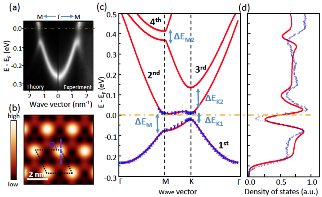
Figure 4.
(a) Comparison between the experimental and calculated ARPES intensity for Ag/Cu(111) showing that both the energy gap width and the intensity of the folded band are reproduced. The spectra have been divided by the Fermi function in order to evidence the spectral weight in the 3 energy range above the Fermi energy; (b) The surface potential built from the and components; (c) The surface band structure (lines) calculated from the experimentally determined surface potential and experimental dispersions (symbols) up to the Fermi energy; (d) Experimental scanning tunneling spectrum (symbols) and calculated local density of states (lines) evidencing the energy gaps of the band structure.
4. Conclusions
In this paper, we show that the peculiar electronic properties usually encountered in hexagonal 2D lattices (i.e., the existence of a gapless Dirac point at K points of the Brillouin zone with linear dispersion) result from the group of wave vectors at this specific high symmetry point. This behavior appears for states belonging to the two dimensional irreducible representation of the corresponding wave vector group. A symmetry breaking that modifies the wave vector group at the K point leads to the opening of an energy gap associated with finite mass Dirac electrons. More precisely, it is related to the breakdown of the mirror symmetry crossing the K point. This behavior is illustrated on the Shockley state of the Ag/Cu(111) reconstructed surface. In this system, the surface electronic properties can be described in the nearly fee electron model. From the measured gap widths, the first Fourier components can be obtained, and the surface potential can be built.
Conflicts of Interest
The authors declare no conflict of interest.
References
- Anderson, P.W. More is different. Science 1972, 177, 393–397. [Google Scholar] [CrossRef] [PubMed]
- Higgs, P.W. Broken symmetries and the masses of gauge bosons. Phys. Rev. Lett. 1964, 13, 508–509. [Google Scholar] [CrossRef]
- Anderson, P.W. Basic Notions of Condensed Matter Physics; The Benjamin/Cummings Publishing Company, Inc.: Menio Park, CA, USA, 1984. [Google Scholar]
- Castro Neto, A.H.; Guinea, F.; Peres, N.M.R.; Novoselov, K.S.; Geim, A.K. The electronic properties of graphene. Rev. Mod. Phys. 2009, 81, 109–162. [Google Scholar] [CrossRef]
- Kogan, E.; Nazarov, V.U. Symmetry classification of energy bands in graphene. Phys. Rev. B 2012, 85, 115418:1–115418:5. [Google Scholar] [CrossRef]
- Starodub, E.; Bostwick, A.; Moreschini, L.; Nie, S.; El Gabaly, F.; McCarty, K.F.; Rotenberg, E. In-plane orientation effects on the electronic structure, stability, and Raman scattering of monolayer graphene on Ir(111). Phys. Rev. B 2011, 83, 125428:1–125428:9. [Google Scholar] [CrossRef]
- Meunier, I.; Tréglia, G.; Gay, J.-M.; Aufray, B.; Legrand, B. Ag/Cu(111) structure revisited through an extended mechanism for stress relaxation. Phys. Rev. B 1999, 59, 10910–10917. [Google Scholar] [CrossRef]
- N’Diaye, A.T.; Bleikamp, S.; Feibelman, P.J.; Michely, T. Two-dimensional Ir cluster lattice on a graphene moiré on Ir(111). Phys. Rev. Lett. 2006, 97, 215501:1–215501:4. [Google Scholar] [CrossRef]
- Reinert, F.; Nicolay, G.; Schmidt, S.; Ehm, D.; Hüfner, S. Direct measurements of the L-gap surface states on the (111) face of noble metals by photoelectron spectroscopy. Phys. Rev. B 2001, 63, 115415:1–115415:7. [Google Scholar] [CrossRef]
- Bendounan, A.; Cercellier, H.; Fagot-Revurat, Y.; Kierren, B.; Yurov, V.Y.; Malterre, D. Modification of Shockley states induced by surface reconstruction in epitaxial Ag films on Cu(111). Phys. Rev. B 2003, 67, 165412:1–165412:10. [Google Scholar] [CrossRef]
- Schiller, F.; Cordón, J.; Vyalikh, D.; Rubio, A.; Ortega, J.E. Fermi gap stabilization of an incommensurate two-dimensional superstructure. Phys. Rev. Lett. 2005, 94, 016103:1–016103:4. [Google Scholar] [CrossRef]
- Bendounan, A.; Forster, F.; Ziroff, J.; Schmitt, F.; Reinert, F. Influence of the reconstruction in Ag/Cu(111) on the surface electronic structure: Quantitative analysis of the induced band gap. Phys. Rev. B 2005, 72, 075407:1–075407:6. [Google Scholar] [CrossRef]
- Bendounan, A.; Forster, F.; Reinert, F.; Kierren, B.; Fagot-Revurat, Y.; Malterre, D. Comment on fermi gap stabilization of an incommensurate two-dimensional superstructure. Phys. Rev. Lett. 2006, 96. [Google Scholar] [CrossRef]
- Ashcroft, N.W.; Mermin, N.D. Solid State Physics; Cengage Learning: Stamford, CT, USA, 1976. [Google Scholar]
- Abd El-Fattah, Z.M.; Matena, M.; Corso, M.; García de Abajo, F.J.; Schiller, F.; Ortega, J.E. Lifshitz transition across the Ag/Cu(111) superlattice band gap tuned by interface doping. Phys. Rev. Lett. 2011, 107, 066803:1–066803:5. [Google Scholar] [CrossRef]
- García de Abajo, F.J.; Cordón, J.; Corso, M.; Schiller, F.; Ortega, J.E. Fermi gap engineering by Au doping of the Ag/Cu(111) dislocation network. Nanoscale 2010, 2, 717–721. [Google Scholar] [CrossRef] [PubMed]
- Vasseur, G.; Fagot-Revurat, Y.; Kierren, B.; Sicot, M.; Malterre, D. Electronic surface potential from angle resolved photoemission. Phys. Rev. B. 2013, in press. [Google Scholar] [CrossRef]
- Malterre, D.; Kierren, B.; Fagot-Revurat, Y.; Pons, S.; Tejeda, A.; Didiot, C.; Cercellier, H.; Bendounan, A. ARPES and STS investigation of Shockley states in thin metallic films and periodic nanostructures. New J. Phys. 2007, 9, 391:1–391:29. [Google Scholar] [CrossRef]
© 2013 by the authors. Licensee MDPI, Basel, Switzerland. This article is an open access article distributed under the terms and conditions of the Creative Commons Attribution license ( http://creativecommons.org/licenses/by/4.0/).