Modeling of Glide-Symmetric Dielectric Structures


Faculty of Electrical Engineering and Computing, University of Zagreb, Unska 3, 10000 Zagreb, Croatia
*
Author to whom correspondence should be addressed.
Symmetry 2019, 11(6), 805; https://doi.org/10.3390/sym11060805
Submission received: 6 May 2019
/
Revised: 11 June 2019
/
Accepted: 12 June 2019
/
Published: 18 June 2019
(This article belongs to the Special Issue Higher Symmetries and Its Application in Microwave Technology, Antennas and Metamaterials)
Abstract
:Recently, there has been an increased interest in exploring periodic structures having higher symmetry properties, primarily based on metallic realization. The design of dielectric glide-symmetric structures has many challenges, and this paper presents a systematic analysis approach based on Floquet mode decomposition and mode matching technique. The presented procedure connects the analysis of standard periodic structures and glide-symmetric realizations, thus giving insight into the wave propagation and interaction characteristics. The obtained results were verified in comparison with results from known references and using a commercial solver, proving that the proposed analysis technique is inherently accurate, and the degree of accuracy depends only on the number of modes used. The proposed analysis approach represents the first step in the design process of dielectric periodic structures with glide symmetry.
1. Introduction
Interest in different artificial electromagnetic structures has led to investigation of various structures, applications and ideas in general. A very promising direction in these developments is structures with higher symmetries. For a periodic structure we can say that it possesses a higher symmetry when the unit cell coincides with itself after more than one geometrical operation of a different kind—translation, rotation, mirroring, etc. [1,2,3]. The glide operator, for example, is a geometrical transformation composed by a translation and a mirroring with respect to the so-called glide plane. The idea to combine different types of symmetry in a periodic structure will have a strong influence on the propagation properties. One of the most interesting is the possibility to tune the dispersion of lower propagating modes depending on the application, i.e., dispersion can be reduced or increased. In addition, as a direct consequence of this, the electromagnetic bandgap can be extended or reduced, or even completely removed.
Periodic structures with higher symmetry were first studied in the 1960s and 1970s in relation to one-dimensional periodic waveguides [1,2,3]. Recent work on structures with higher symmetries (in both one and two dimensions) has demonstrated various effects and devices, such as ultra-wideband Luneburg lenses [4,5], leaky-wave antennas with low frequency dependency [6], cost-efficient gap waveguide technology [7,8], contactless flanges with low leakage [9], low-dispersive propagation in periodic structure-based transmission lines [10,11], and fully metallic reconfigurable filters and phase shifters [12]. These results were obtained using metallic structures, however, in many applications only dielectric types of materials are allowed. Therefore, our interest lies in the investigation of the fully dielectric structures with higher symmetry.
Dielectric waveguides containing periodic variation along the propagation direction have been used in many applications ranging from microwave to optical frequencies. They are designed to either support a bounded propagating wave (in microwave or optical filters and distributed feedback reflectors for high-quality lasers) or an unbounded leaky wave (in leaky-wave antennas and optical couplers) [13]. Recently, some new applications were investigated, like plasmonic optical modulators for nanophotonic architectures in which the modulator transmittance is changed with bias voltage [14].
The reported analysis methods were often based on the assumption that periodic variation acts only as a small perturbation of a planar multilayer waveguide [15,16,17], which may produce erroneous results in many cases, e.g., if the corrugated grating is thick. The proposed rigorous solution is based on the Floquet mode decomposition and a mode matching (MM) technique [18,19] in which the corrugated layer is modeled as a periodic array of infinite dielectric slabs [20]. All previously considered structures contained one layer of corrugations, except in Reference [21] where two layers of corrugations with different periodicities were investigated. The Floquet mode expansion approach can also be combined with the boundary integral formulation in which the boundary conditions at each interface inside the structure follow Floquet’s theorem [22]. Similarly, the finite element method can be adapted for computation of modal decomposition and scattering matrices [23,24].
In this paper we have extended the MM analysis method to glide-symmetric dielectric periodic structures. The presented analysis description is focused on one-dimensional glide-symmetric structures [25]. The first part of the paper describes the analysis procedure and it is followed by initial results obtained for a test case found in literature, while the properties of the glide-symmetric dielectric structures are discussed in the second part of the paper.
2. Analysis of Waveguides Containing Periodic Dielectric Structures
A periodic structure possesses a higher symmetry when the unit cell coincides with itself after more than one geometrical operation. Glide symmetry is the invariance of a periodic structure under a translation of half its period and a mirroring with respect to a plane parallel to the periodicity directions. Written as a formula, if the periodicity is present along the x-direction with the period Px, a glide operator can be written as:
Other kinds of higher symmetries are defined by combination of rotation and translation (twist or polar glide symmetries) or by time operations (parity-time symmetries).
The analysis of guiding dielectric structures having higher symmetries is based on Floquet mode decomposition and MM approach [26,27,28,29]. The electric and magnetic fields in each section of the structure are represented as a sum of suitable modes with unknown complex amplitude, i.e., we used the preknowledge about the electromagnetic (EM) field configuration and symmetry properties to reduce the number of unknowns, to precisely describe the EM field present in the structure, and to give a physical insight about the presence of higher symmetry properties.
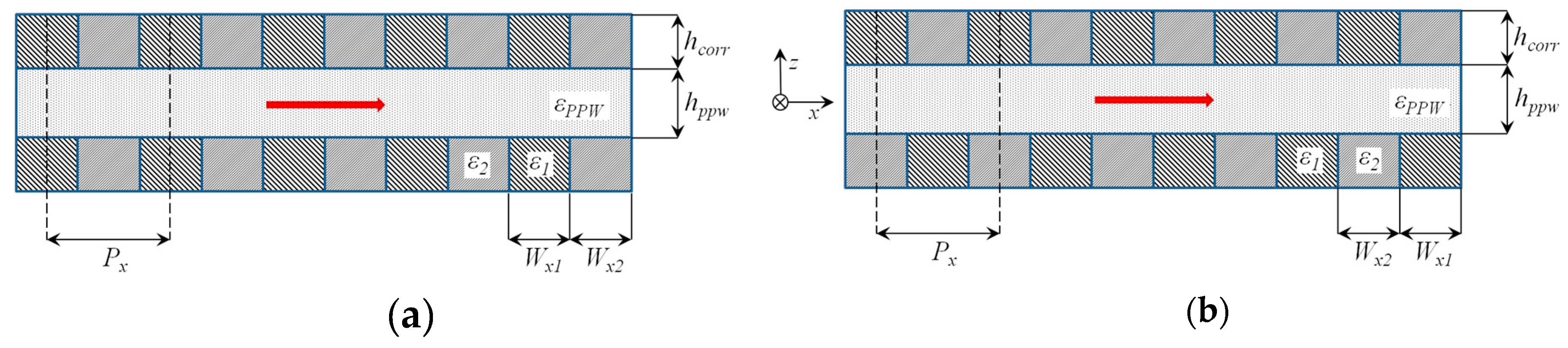
The dielectric waveguide structure of interest is shown in Figure 1. It is a parallel-plate waveguide (PPW) with top and bottom walls realized using dielectric corrugations. The period of corrugations is denoted by Px, the height of corrugations by hcorr, the width and permittivity of periodic dielectric inclusions by Wx1, Wx2 and ε1, ε2, and the height and permittivity of parallel-plate waveguide by hppw and εppw. Note that the plane z = 0 is located in the middle of the parallel-plate region. We will first analyze the simple periodic structure (i.e., the one with classical translation/mirroring symmetry, see Figure 1a) and then we will modify the analysis procedure for structures with higher symmetry in which the corrugations are shifted with respect to each other by Px/2, i.e., the structure will be glide-symmetric, as in Figure 1b.
The waveguide mode of interest is propagating in the direction perpendicular to corrugations (i.e., in the x-direction). Therefore, we can distinguish transverse electric (TE) and transverse magnetic (TM) propagating modes (i.e., they do not mix due to presence of the periodic structure corrugations). Here we will give the formulation for TE modes because it is straightforward to repeat the formulation for TM modes.
The analysis is based on representation of the EM field in all regions of interest: Parallel-plate region, layer with corrugations, and outer space. The analysis procedure can be simplified if the modes are orthogonal. This is enforced in the parallel-plate waveguide region by representing the EM field as a series of Floquet harmonics by virtue of periodicity. For each Floquet mode present in the parallel-plate waveguide the y-component of the E-field can be expressed as
The tangential x-component of H-field can be calculated using the following expression
Here, m is the index of the Floquet mode, NPPW is the highest-order considered Floquet mode (in total 2NPPW + 1 modes are taken into account), and k0 and η0 are the wave number and the wave impedance of free space.
In order to determine the Floquet coefficients Am and the propagation constant kx,0 of the propagating wave inside the parallel-plate waveguide we need to match the tangential EM components with the ones in the corrugated walls. The wave propagating in the corrugated region can be modeled as a wave propagating along a periodic array of dielectric slabs [18,20] with the following EM field distribution (Ncorr denotes the highest-order considered mode).
The coefficients and the propagation constant in the z-direction γi are determined by considering the wave propagation along the periodic array with an assumed progressive phase delay per unit cell. In more detail, for each possible propagation constant kx,0, i.e., for each considered progressive phase delay we need to solve the secondary (local) mode-matching problem. The problem is described with a linear system of four equations representing the continuity of the Ey and Hz field components at two boundaries x = ±W1/2. Since for each considered case we have six unknown coefficients as seen in Equations (5)–(7), the Floquet theorem is used to express and using , and assuming progressive phase delay. The determinantal equation resulting from the linear system gives the value of the propagation constant along the interfaces γi and then it is possible to determine the field distribution of the considered ith mode. The details of the formulation are given in Reference [18].
By matching these two expressions (e.g., for the E-field at the boundary z = hppw/2) and testing it with , one equation per each Floquet harmonic is obtained (as a consequence of orthogonality of Floquet harmonics):
We can further simplify Equation (8) by considering only even or odd modes (with respect to the symmetry plane z = 0). By doing so, only one coefficient or is left and we have consequently expressed each Floquet coefficient Am with the Fourier transformation of the E-field distribution at the corrugation boundary. Thereby, only the coefficients (among all coefficients Am, Bi, Ci and Dm that describe the field distribution) are the unknowns.
The goal is to derive one characteristic equation for the propagation constant kx,0 of the propagating wave inside the parallel-plate waveguide. Therefore, we should also match the tangential magnetic field Hx at the boundary between parallel-plate waveguide and corrugated region.
Equation (10) can be simplified using the connection between the coefficients Am and (given by Equations (8) and (9)). By multiplying Equation (10) with , where * refers to the complex conjugate, and integrating over the period we obtain the following linear system of equations whose determinant is the characteristic equation for the propagation constant kx,0
The coefficients of the linear system of equations related to the unknowns and are respectively equal (e.g., for the even symmetry case)
Note that the field distributions of the propagating modes along the periodic array of dielectric slabs (i.e., along the corrugations) are not orthogonal.
Since we have two times more unknowns than equations, we have to repeat the procedure for the half-space above the corrugations. The EM field in the upper half-space (i.e., in the space outside the structure) can be represented as:
Here, we have assumed that the space outside the structure is air (or vacuum) with the relative permittivity equal to one. The corresponding coefficients of the linear system of equations related to the unknown are equal
It is enough to consider only the upper half of the structure shown in Figure 1a; the lower part is taken into account using even or odd mirroring symmetry of the considered modes.
For the structures with glide symmetry, i.e., if the upper corrugated plate is shifted by half a period in the x-direction, the E-field distributions at the top and bottom corrugation interfaces can be related as:
This expression should have the double sign ± in front of the exponential term. However, the double sign ± does not define two different sets of modes or introduce any ambiguity because the solutions of the two problems actually coincide: the Floquet harmonic 0 becomes the harmonic −1 when switching the sign from plus to minus (see Reference [28] for details).
We will use the following translation property of the Fourier transformation:
Term actually means that depending on the index of Floquet mode we have even or odd symmetry across the z = 0 plane (see Equation (2)). For even Floquet modes the E-field in the parallel-plate region is described with terms, while for odd Floquet modes the E-field is described with terms. In other words, the presence of glide symmetry causes the odd and even symmetries to be mixed inside the PPW resulting in extraordinary properties of the glide-symmetric guiding structure.
3. Results
In order to test the developed code, we compared the results of a calculated field distribution inside the corrugated layer with the results from [18]. We plotted the normalized value of the Hy field component of the TM wave for different values of assumed progressive phase delay per unit cell. The parameters of the corrugated structure are the following: εr1 = 2.56, εr2 = 1.0, Px = 0.6 λ0, Wx1 = 0.26 λ0 and Wx2 = 0.34 λ0. Excellent matching of the obtained results can be noticed in Figure 2. We also tested the accuracy of the calculated propagation constant of the first two modes travelling along the periodic array of dielectric slabs (Figure 3). Again we got excellent agreement with results given in [18]. It is interesting to notice that for values kx,0 less than 0.5·π/Px the first high-order mode is evanescent, i.e., the values of γ2 are imaginary (kx,0 is the transverse propagation constant in the corrugated region). For values kx,0 larger than 0.5·π/Px the wave propagates along the dielectric slabs and consequently γ2 is a real number. The dominant mode is of a propagating type for all values of kx,0.
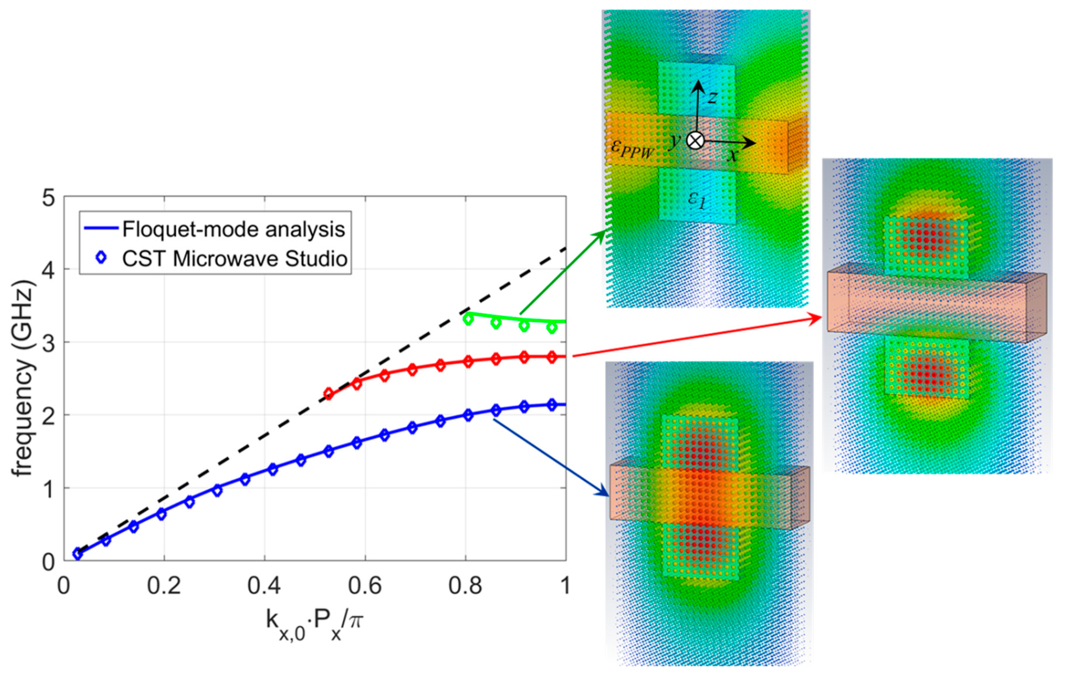
In order to investigate the properties of glide-symmetric dielectric structures we considered the following periodic structure: εPPW = 2.56, hPPW = 10 mm, Px = 35 mm, Wx1 = 15 mm, Wx2 = 20 mm, εr1 = 10.0, εr2 = 1.0, and hcorr = 10 mm. First, we analyzed the simple periodic structure (Figure 1a). In Figure 4 the dispersion diagram of the first three propagating modes are given. Note that only the values of the propagation constant larger than the free-space propagation constant k0 are given, otherwise the excited mode is a fast wave and the structure is radiating part of the EM energy (i.e., we have a leaky-wave antenna). The obtained results were compared with the ones obtained using a general electromagnetic solver, CST Microwave Studio in our case, and the agreement is very good. Specifically, the Eigenmode Solver in the CST Microwave Studio package was used to find the dispersion characteristics of the considered structures, thus it was necessary to analyze only a unit cell. In x- and y- directions the periodic boundary conditions were applied, while at the top and bottom of the periodic cell the PMC boundary conditions were used to simulate infinitely long symmetric and glide-symmetric structures. Note that the unit cell was quite long in the z-direction since it was needed to ensure that the amplitude of the evanescent fields was negligible at the top and bottom boundaries.
In Figure 4 the field distributions of the first three propagating modes are also given. Note that the dominant mode is even (relative to the symmetry line z = 0), the first higher order-mode is odd, and the second higher-order mode is even again. Note also that the evanescent field is present also in the air close to the structure. This is probably the most important difference compared to the metallic waveguides. The higher the mode (or for frequencies closer to the cut-off frequency), the larger the percentage of the power actually propagating out of the parallel-plate waveguide and consequently in the half-spaces around the guiding structure. In Figure 4, the third mode has more than half of the power propagating outside the waveguiding structure. Theoretically, for frequencies just above cut-off almost all power is actually propagating outside the parallel-plate layer [30]. This is one of the limits in the design of dielectric glide-symmetric structures since the designed metallic components mostly have a very thin parallel-plate region (in order to obtain the desired electromagnetic properties). In the dielectric case probably there is no point to make equivalent structures with a thin gap between corrugations since almost all power will propagate outside the guiding structure.
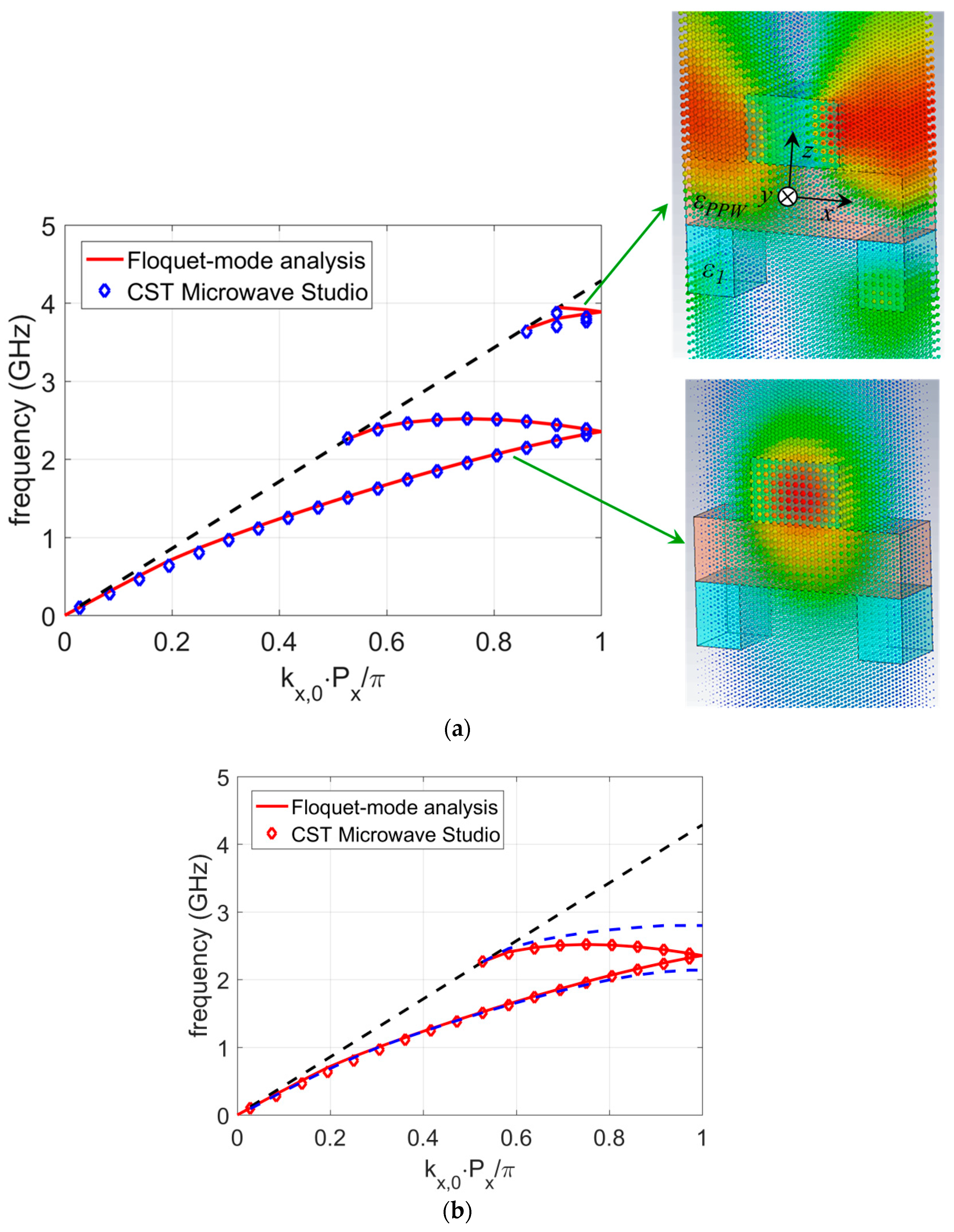
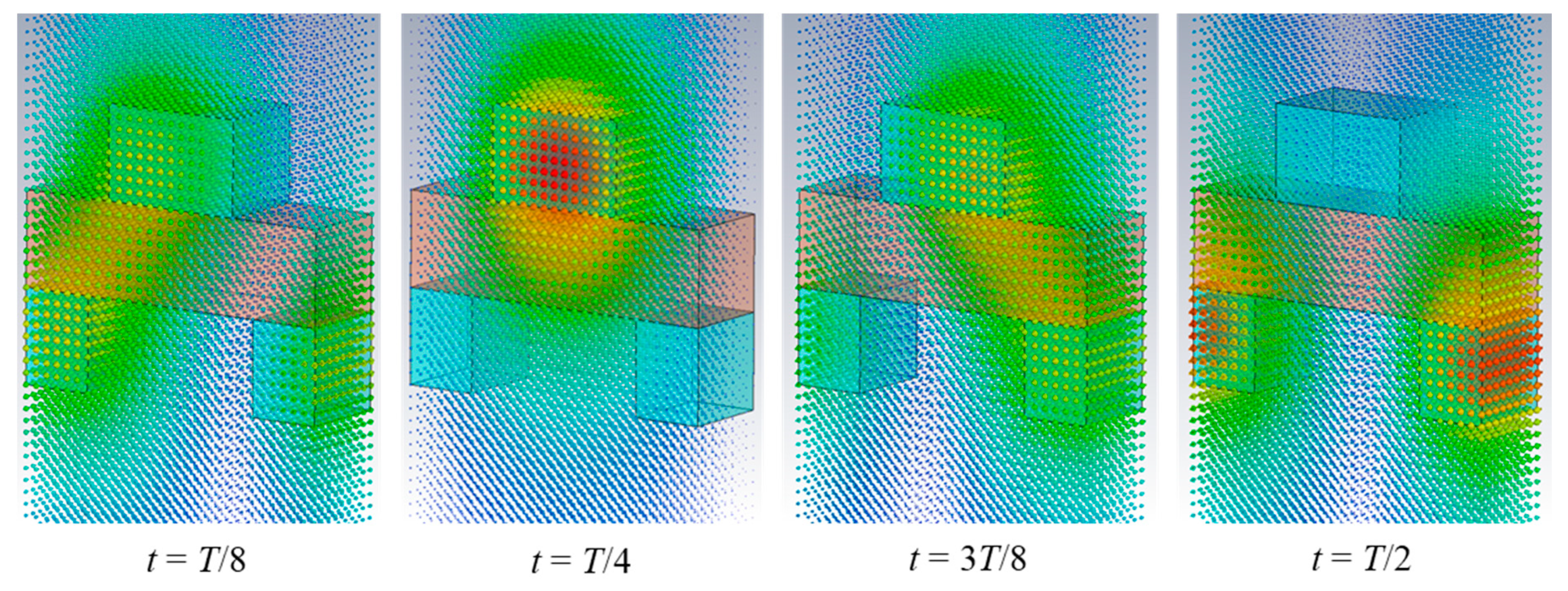
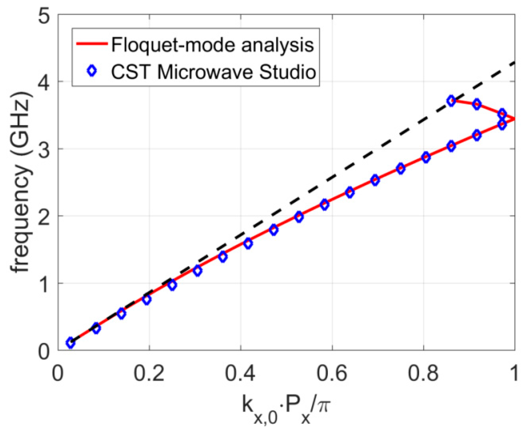
The dispersion diagram of the glide-symmetric dielectric waveguide (having the same dimensions as considered simple periodic structure) is given in Figure 5. The shape of the obtained dispersion diagram is similar to the ones obtained with metallic glide-symmetric waveguides. The obtained bandgap is between 2.52 and 3.65 GHz. The field distribution of the first two modes is also shown for kx,0 = π/Px. Like in the case of the simple periodic structure (Figure 4) a much larger percentage of EM power is propagating outside the dielectric structure for the second mode. The selected time moment gives the best illustration of the E-field distribution for the depicted modes. Other time moments could be selected, as illustrated in Figure 6 where the E-field distribution of the dominant mode is given for relative phase shifts 45°, 90°, 135° and 180°, respectively.
In order to be able to tune the dispersion diagram according to the designer’s needs one should understand the background of such a shape. The key point is Equation (19), i.e., the fact that glide symmetry actually means mixing of odd and even modes. This is visible in Figure 5b where we have displayed on the same diagram dispersion curves of simple and glide-symmetric dielectric waveguides. It can be seen that the lower part of the dispersion curve is nearly indistinguishable from the even mode profile of the non-glide structure (up to the vicinity of the propagation constant kx,0 = π/Px), while the upper part is mostly affected by the odd mode.
This property actually enabled us to tune the dispersion diagram (see Figure 7). For example, if we reduced the thickness of the parallel-plate region from 10 mm to 2 mm, then the odd mode had a higher cut-off frequency and therefore the dispersion diagram of a glide-symmetric case was less dispersive and the bandgap started at higher frequencies. This was even more prominent if we reduced the thickness of the corrugated region from 10 mm to 2 mm (Figure 7b) because the overall thickness of the dielectric structure was then much smaller.
We tested various combinations of refractive indexes for PPW and corrugated regions. One natural choice is to have only one material, i.e., that corrugations are made from the same material as the PPW (εr1 = εPPW = 2.56 and εr2 = 1.0; other parameters are the same as for the structure in Figure 5). In other words, such structures are made from a homogeneous media but the boundaries have a periodic variation. Results of the same type were obtained (see Figure 8), however the glide-symmetric properties were not so pronounced. It can be concluded that contrast between the permittivity of PPW and corrugated regions can also be used for tuning the dispersion properties.
Needless to say, it is possible to analyze guiding structures in which the lower corrugated layer is arbitrarily shifted compared to the upper layer (i.e., when the shift is between 0 and Px/2). The obtained dispersion diagrams are located between ones for the symmetric and glide-symmetric cases, which was demonstrated in Reference [11] for metallic structures. Therefore, we have focused our investigation on the two most interesting cases, symmetric and glide-symmetric.
Finally, numerical properties of the proposed analysis method should be mentioned. The number of modes in the PPW and corrugated regions were NPPW = 5 (in total 11 modes) and Ncorr = 2. We tested the numerical convergence of the solution, and enlarging the number of modes only slightly improved the accuracy of the solution. The needed computer time was less than a second per point in the dispersion diagram, while the CST typically needed around 1 hour for calculating the whole dispersion diagram (depending on the accuracy of the meshing). All the calculations were made on a standard PC.
4. Conclusions
This paper discussed the Floquet mode decomposition applied together with a mode-matching approach in the analysis and design of dielectric waveguides with glide-symmetric periodicity. The analysis method is based on representing the EM field in each region with suitable modes and connecting the field distributions in different regions using symmetry properties, resulting in an efficient program for determining propagation properties and obtaining a physical picture of modes in such waveguides. The developed approach provides a basis for better understanding of wave propagation characteristics and of various types of wave interactions in glide-symmetric structures.
Until now most realized waveguide prototypes possessing higher symmetry were made from metal. Although at first glance there are a lot of similarities between metallic and dielectric glide-symmetric structures, the main difference comes from the fact that in the dielectric case, part of the propagating wave (and thus part of the electromagnetic power) travels outside the dielectric parallel-plate waveguide. Therefore, the dispersion diagram (and consequently the bandgap) is dominantly conditioned by the odd mode of the equivalent non-glide structure whose cut-off frequency mostly depends on the total thickness and permittivity of the waveguide structure. This also limits us in selecting the thickness of the parallel-plate waveguide since the percentage of power propagating outside the guiding structure is larger for thinner structures. The other limit represents the free-space wavenumber—for propagation constants smaller than the free-space wavenumber a fast wave is excited which leads to leakage of electromagnetic energy. Our presented discussion shows that by adjusting the structure parameters various waveguiding properties can be obtained, and our formulation is able to aid in the design process and provide fast and accurate results.
Author Contributions
The contributions of both authors were approximately the same. Both authors worked together to develop the present manuscript.
Funding
This work was funded by Croatian Science Foundation under the project IP-2018-01-9753.
Conflicts of Interest
The authors declare no conflict of interest.
References
- Crepeau, P.J.; McIsaac, P.R. Consequences of symmetry in periodic structures. Proc. IEEE 1964, 52, 33–43. [Google Scholar] [CrossRef] [Green Version]
- Mittra, R.; Laxpati, S. Propagation in a waveguide with glide refection symmetry. Can. J. Phys. 1965, 43, 353–372. [Google Scholar] [CrossRef]
- Hessel, A.; Chen, M.H.R.; Li, C.M.; Oliner, A.A. Propagation in periodically loaded waveguides with higher symmetries. Proc. IEEE 1973, 61, 183–195. [Google Scholar] [CrossRef]
- Quevedo-Teruel, O.; Ebrahimpouri, M.; Ng Mou Kehn, M. Ultrawideband Metasurface Lenses Based on Off-Shifted Opposite Layers. IEEE Antennas Wirel. Propag. Lett. 2016, 15, 484–487. [Google Scholar] [CrossRef]
- Quevedo-Teruel, O.; Miao, J.; Mattsson, M.; Algaba-Brazalez, A.; Johansson, M.; Manholm, L. Glide-Symmetric Fully Metallic Luneburg Lens for 5G Communications at Ka-Band. IEEE Antennas Wirel. Propag. Lett. 2018, 17, 1588–1592. [Google Scholar] [CrossRef]
- Dahlberg, O.; Pucci, E.; Wang, L.; Quevedo-Teruel, O. Low-Dispersive Glide-Symmetric Leaky-Wave Antenna at 60 GHz. In Proceedings of the 13th European Conference on Antennas and Propagation, Krakow, Poland, 31 March–5 April 2019. [Google Scholar]
- Ebrahimpouri, M.; Quevedo-Teruel, O.; Rajo-Iglesias, E. Design guidelines for gap waveguide technology based on glide-symmetric holey structures. IEEE Microw. Wirel. Compon. Lett. 2017, 27, 542–544. [Google Scholar] [CrossRef]
- Ebrahimpouri, M.; Rajo-Iglesias, E.; Sipus, Z.; Quevedo-Teruel, O. Cost-effective gap waveguide technology based on glide-symmetric holey EBG structures. IEEE Trans. Microw. Theory Tech. 2018, 66, 927–934. [Google Scholar] [CrossRef]
- Ebrahimpouri, M.; Algaba-Brazalez, A.; Manholm, L.; Quevedo-Teruel, O. Using glide-symmetric holes to reduce leakage between waveguide flanges. IEEE Microw. Wirel. Compon. Lett. 2018, 28, 473–475. [Google Scholar] [CrossRef]
- Padilla, P.; Herran, L.F.; Tamayo-Dominguez, A.; Valenzuela-Valdes, J.F.; Quevedo-Teruel, O. Glide symmetry to prevent the lowest stopband of printed corrugated transmission lines. IEEE Microw. Wirel. Compon. Lett. 2018, 28, 750–752. [Google Scholar] [CrossRef]
- Quesada, R.; Martín-Cano, D.; García-Vidal, F.J.; Bravo-Abad, J. Deep subwavelength negative-index waveguiding enabled by coupled conformal surface plasmons. Opt. Lett. 2014, 39, 2990–2993. [Google Scholar] [CrossRef] [PubMed]
- Rajo-Iglesias, E.; Ebrahimpouri, M.; Quevedo-Teruel, O. Wideband phase shifter in groove gap waveguide technology implemented with glide-symmetric holey EBG. IEEE Microw. Wirel. Compon. Lett. 2018, 28, 476–478. [Google Scholar] [CrossRef]
- Elachi, C. Waves in active and passive periodic structures: A review. Proc. IEEE 1976, 64, 1666–1698. [Google Scholar] [CrossRef] [Green Version]
- Babicheva, V.E.; Lavrinenko, A.V. Plasmonic modulator optimized by pattering of active layer and tuning permittivity. Opt. Commun. 2012, 285, 5500–5507. [Google Scholar] [CrossRef]
- Hope, L.L. Theory of optical grating couplers. Opt. Commun. 1972, 11, 2234–2241. [Google Scholar] [CrossRef]
- Harris, J.A.; Winn, R.K.; Dalgoutte, D.G. Theory and design of periodic couplers. Appt. Opt. 1972, 11, 2234–2241. [Google Scholar] [CrossRef] [PubMed]
- Stolland, H.; Yariv, A. Coupled-mode analysis of periodic dielectric waveguides. Opt. Commun. 1973, 8, 5–8. [Google Scholar] [CrossRef]
- Peng, S.T.; Tamir, T.; Bertoni, H.L. Theory of periodic dielectric waveguides. IEEE Trans. Microw. Theory Tech. 1975, 23, 123–133. [Google Scholar] [CrossRef]
- Peng, S.T. Rigorous formulation of scattering and guidance by dielectric grating waveguides: General case of oblique incidence. J. Opt. Soc. Am. A 1989, 6, 1869–1883. [Google Scholar] [CrossRef]
- Lewis, L.R.; Hessel, A. Propagation characteristics of periodic arrays of dielectric slabs. IEEE Trans. Microw. Theory Tech. 1971, 19, 276–286. [Google Scholar] [CrossRef]
- Peng, S.T. Rigorous analysis of guided waves in doubly periodic structures. J. Opt. Soc. Am. A 1990, 7, 1448–1456. [Google Scholar] [CrossRef]
- Hadjicostas, G.; Butler, J.K.; Evans, G.A.; Carlson, N.W.; Amantea, R. A numerical investigation of wave interaction in dielectric waveguides with periodic surface corrugations. IEEE J. Quantum Electron. 1990, 26, 893–902. [Google Scholar] [CrossRef]
- Bao, G. Finite element approximation of time harmonic waves in periodic structures. SIAM J. Numer. Anal. 1995, 32, 1155–1169. [Google Scholar] [CrossRef]
- Dossou, K.; Byrne, M.A.; Botten, L.C. Finite Element Computation of Grating Scattering Matrices and Application to Photonic Crystal Band Calculations. J. Comput. Phys. 2006, 219, 120–143. [Google Scholar] [CrossRef]
- Valerio, G.; Sipus, Z.; Grbic, A.; Quevedo-Teruel, O. Accurate equivalent-circuit descriptions of thin glide-symmetric corrugated metasurfaces. IEEE Trans. Antennas Propag. 2017, 65, 2695–2700. [Google Scholar] [CrossRef]
- Wexler, A. Solution of waveguide discontinuities by modal analysis. IEEE Trans. Microw. Theory Tech. 1967, 15, 508–517. [Google Scholar] [CrossRef]
- Clarricoats, P.J.B.; Slinn, K.R. Numerical method for the solution of waveguide-discontinuity problems. Electron. Lett. 1966, 2, 226–228. [Google Scholar] [CrossRef]
- Valerio, G.; Ghasemifard, F.; Sipus, Z.; Quevedo-Teruel, O. Glide-Symmetric All-Metal Holey Metasurfaces for Low-Dispersive Artificial Materials: Modeling and Properties. IEEE Trans. Microw. Theory Tech. 2018, 66, 3210–3223. [Google Scholar] [CrossRef] [Green Version]
- Ghasemifard, F.; Norgren, M.; Quevedo-Teruel, O.; Valerio, G. Analyzing Glide-Symmetric Holey Metasurfaces Using a Generalized Floquet Theorem. IEEE Access 2018, 6, 71743–71750. [Google Scholar] [CrossRef]
- Okamoto, K. Fundamentals of Optical Waveguides, 2nd ed.; Academic Press: Cambridge, MA, USA, 2006. [Google Scholar]
Figure 1.
Sketch of the parallel-plate dielectric waveguide with periodic structure; (a) simple periodic structure with translation and mirroring symmetry, and (b) periodic structure with glide symmetry. Direction of wave propagation is sketched using a red arrow.
Figure 1.
Sketch of the parallel-plate dielectric waveguide with periodic structure; (a) simple periodic structure with translation and mirroring symmetry, and (b) periodic structure with glide symmetry. Direction of wave propagation is sketched using a red arrow.

Figure 2.
Normalized value of the H field component of TM wave for different values of assumed progressive phase delay per unit cell; solid line—results calculated using the developed program, diamonds—calculated results from [18]; (a) first mode, (b) second mode.
Figure 2.
Normalized value of the H field component of TM wave for different values of assumed progressive phase delay per unit cell; solid line—results calculated using the developed program, diamonds—calculated results from [18]; (a) first mode, (b) second mode.

Figure 3.
Normalized value of the propagation constant of the first two modes travelling along the periodic array of dielectric slabs; solid line—results calculated using the developed program, diamonds—calculated results from Reference [18]. γ2 = 0 is the cut-off condition of the 2nd mode, thus for the values kx,0 smaller than the cut-off value (0.5·π/Px) γ2 is imaginary (the mode is evanescent).

Figure 4.
Propagation constant of the first three modes travelling along the dielectric waveguide with corrugations from Figure 1a; solid line—results calculated using the developed program (blue line: 1st even mode, red line: 1st odd mode, green line: 2nd even mode), diamonds—results calculated using CST Microwave Studio (dashed black line represents the light-line). The E-field distribution in the unit cell of the first three modes for kx,0 = π/Px is also shown (the structure is infinite in the y-direction).

Figure 5.
Propagation constant of the first two modes travelling along the glide-symmetric dielectric waveguide with corrugations (Figure 1b); solid line—results calculated using the developed program, diamonds—results calculated using CST Microwave Studio (dashed black line represents the light-line); (a) glide-symmetric structure only, (b) comparison of glide-symmetric and simple-symmetric structures (blue dashed line). The E-field distribution in the unit cell of the first two modes for kx,0 = π/Px is also shown (the structure is infinite in the y-direction).

Figure 6.
The E-field distribution in the unit cell of the first mode for kx,0 = π/Px at different time moments where T denotes the period of oscillations (T = 1/f).
Figure 6.
The E-field distribution in the unit cell of the first mode for kx,0 = π/Px at different time moments where T denotes the period of oscillations (T = 1/f).

Figure 7.
Propagation constant of the first mode travelling along the glide-symmetric dielectric waveguide with corrugations (case of thinner parallel-plate dielectric slab); solid line—results calculated using the developed program, diamonds—results calculated using CST Microwave Studio (dashed black line represents the light-line); (a) case of thinner parallel-plate dielectric slab (hppw = 2 mm), (b) case of thinner corrugated region (hcorr = 2 mm).

Figure 8.
Propagation constant of the first mode travelling along the glide-symmetric dielectric waveguide with corrugations made from homogeneous material; solid line—results calculated using the developed program, diamonds—results calculated using CST Microwave Studio (dashed black line represents the light-line).

© 2019 by the authors. Licensee MDPI, Basel, Switzerland. This article is an open access article distributed under the terms and conditions of the Creative Commons Attribution (CC BY) license (http://creativecommons.org/licenses/by/4.0/).
Share and Cite
MDPI and ACS Style
Sipus, Z.; Bosiljevac, M. Modeling of Glide-Symmetric Dielectric Structures. Symmetry 2019, 11, 805. https://doi.org/10.3390/sym11060805
AMA Style
Sipus Z, Bosiljevac M. Modeling of Glide-Symmetric Dielectric Structures. Symmetry. 2019; 11(6):805. https://doi.org/10.3390/sym11060805
Chicago/Turabian StyleSipus, Zvonimir, and Marko Bosiljevac. 2019. "Modeling of Glide-Symmetric Dielectric Structures" Symmetry 11, no. 6: 805. https://doi.org/10.3390/sym11060805
Note that from the first issue of 2016, this journal uses article numbers instead of page numbers. See further details here.