Strain Effects in Gallium Nitride Adsorption on Defective and Doped Graphene: First-Principles Calculations


1
School of Mechanical and Electrical Engineering, Wuhan University of Technology, Wuhan 430070, China
2
Department of Electrical Engineering and Computer Science, University of Michigan, Ann Arbor, MI 48109, USA
3
School of Mechanical Science and Engineering, Huazhong University of Science and Technology, Wuhan 430074, China
4
Institute of Technological Sciences, Wuhan University, Wuhan 430072, China
5
School of Power and Mechanical Engineering, Wuhan University, Wuhan 430072, China
*
Authors to whom correspondence should be addressed.
Crystals 2018, 8(2), 58; https://doi.org/10.3390/cryst8020058
Submission received: 12 December 2017
/
Revised: 15 January 2018
/
Accepted: 24 January 2018
/
Published: 26 January 2018
(This article belongs to the Special Issue Graphene Mechanics)
Abstract
:Transferable, low-stress gallium nitride grown on graphene for flexible lighting or display applications may enable next-generation optoelectronic devices. However, the growth of gallium nitride on graphene is challenging. In this study, the adsorptions of initial nucleation process of gallium nitride on graphene were investigated using first-principles calculations based on density functional theory. The adsorption energies and the role of in-plane strains were calculated for different possible configurations of the adatoms on the surfaces of vacancy defect and doped graphene. Compared with the results of the gallium adatom, adsorption of the nitrogen atom on graphene was found to exhibit greater stability. The calculations reveal that the vacancy defect core enhanced the adsorption stability of the adatom on graphene, whereas the incorporation of oxygen impurity greatly reduced the stable adsorption of the gallium and nitrogen adatoms. Furthermore, the calculations of strain showed that the lattice expansion led to increased stability for all adsorption sites and configuration surfaces, except for the nitrogen adatom adsorbed over the gallium atom in Ga-doped graphene. The study presented in this paper may have important implications in understanding gallium nitride growth on graphene.
1. Introduction
Graphene, a novel two-dimensional material, has attracted intensive research interest since its discovery in 2004 [1]. Graphene is stable at high-temperature and has a highly oriented honeycomb structure, which can serve as a suitable epitaxial template for the growth of wurtzite semiconductor materials [2]. Gallium nitride (GaN) and related III-nitride semiconductors are regarded as promising materials in the past decades for applications in optoelectronic and electronic devices, such as light emitting diodes (LEDs) [3], laser diodes (LDs) [4], and high electron mobility transistors (HEMTs) [5]. Due to the limited availability of native substrate, GaN and related alloys have been typically deposited heterogeneously on sapphire, silicon carbide (SiC), and silicon substrates [6]. The preparation of GaN on cheaper and larger substrates has attracted much attention. The use of graphene as a substrate for GaN deposition has gained much attention due to the hexagonal arrangement of the sp2 hybridized carbon atoms, which is similar to the c-plane of wurtzite GaN [7,8]. In addition, the lattice mismatch may not be considered seriously as a result of the potential for van der Waals bonding at the GaN/graphene interface [9]. Currently, large-area graphene films can be synthesized by chemical vapor deposition (CVD) processes. Graphene films are also transferable to amorphous or flexible materials [10,11]. Therefore, transferable, low-stress GaN grown on graphene for flexible lighting or display applications may enable next-generation optoelectronic devices.
Despite the potential advantages, the growth of GaN on the basal plane pristine graphene is challenging, largely because of the absence of dangling bonds, which leaves the graphene surface chemically inert [7,12]. Ohta et al. have developed a new thin film growth technique called pulsed sputtering deposition (PSD) and obtained crystalline GaN films on amorphous substrates with the use of graphene buffer layers [13]. He et al. have grown low threading dislocation density GaN films on graphene by hydride vapor phase epitaxy (HVPE) and shown that the crystallinity of GaN layers with a graphene interlayers was improved by inserting a graphene mask structure [14]. Sung et al. employed graphene directly grown on silicon or sapphire substrate as a platform for the growth and lift-off of GaN-based light-emitting diode epitaxial layers, which is useful for not only recycling the substrate but also transferring the epitaxial layer to other flexible substrates [15]. Heilmann et al. presented single-layer graphene as an atomically thin buffer layer for c-axis-oriented growth of vertically aligned GaN nanorods mediated by nanoscale AlGaN nucleation islands [16]. Despite the growing interests in the heteroepitaxy of GaN films on graphene, there have been limited studies aimed at understanding the initial nucleation process. Nitrogen or gallium atoms may be incorporated into carbon vacancies to form a doped configuration when GaN is grown on defective graphene. Oxygen atoms may also be incorporated into carbon vacancies when water vapor is present in the growth environment. Although substitutional doping of oxygen atoms in graphene is unlikely [17], in some cases, the presence of oxygen functionalities at the graphene surface provides reactive sites for the nucleation and growth of nanoparticles [18,19]. Since vacancy defects and incorporation of impurity atoms are inevitable in the fabrication of graphene, the adsorption of GaN atoms on various graphene surfaces can have a significant impact on subsequent growth. Moreover, heterogeneous substrates often induce strain on the surface of graphene [20,21]. Thus, it is essential to understand the effect of surface strain on the adsorption of gallium and nitrogen atoms on graphene.
In this paper, the adsorption of GaN was investigated with the goal of studying the effect of vacancy defects and incorporation of impurity atoms in graphene by performing first-principles calculations. In addition, the influence of strain on GaN adsorption on graphene is reported. The results presented in this paper may have important implications in understanding GaN growth on graphene during the initial growth process.
2. Method and Model
Our first-principles calculations were performed by using the Car–Parrinello molecular dynamics (CPMD) method [22], which have been successfully used for the study of atom and molecular adsorptions [23,24]. The CPMD code is an implementation of DFT in the Kohn–Sham (KS) formulation and of the Car–Parrinello scheme. In the present work, the interactions of the ion cores with the valence electrons were described by Trouiller–Martins norm-conserving pseudo potentials [25], and non-local core corrections (NLCC) were included for the gallium species [26]. The electronic wavefunctions were expanded in a plane wave basis set with an energy cutoff of 80 Ry. The total energy was converged to 10−5 eV. The exchange functional given by Becke [27] and correlation energy expression by Lee–Yang–Parr (LYP) [28] were used with the implementation of local density approximation (LDA) [29]. The Monkhorst–Pack scheme with uniform mesh points was applied in this calculation.
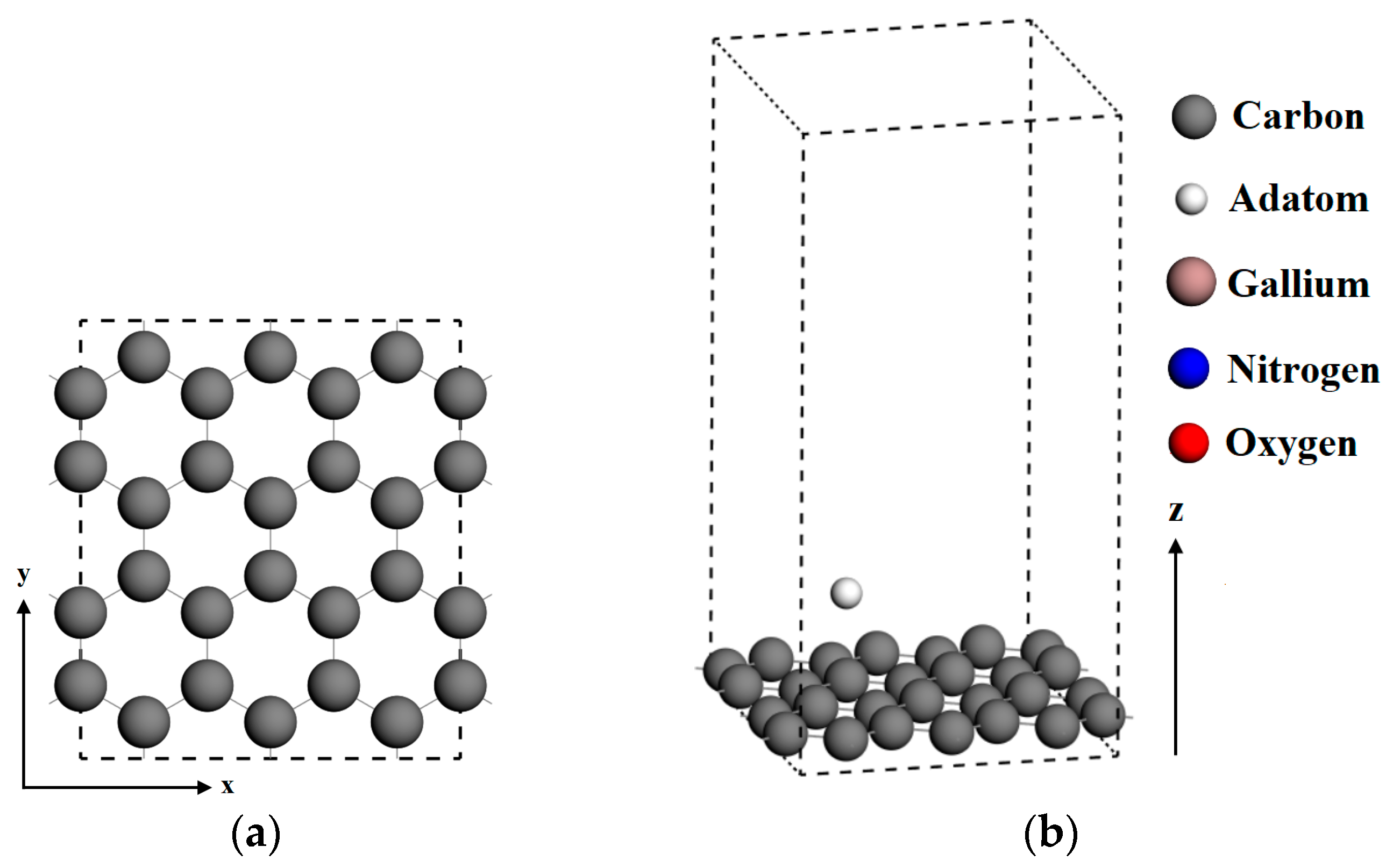
The initial configuration of the graphene supercell was modeled by 3 × 2 of represented graphene unit cells with 24 carbon atoms, where the x-axis corresponds to the zigzag direction and the y-axis is along the armchair direction, as shown in Figure 1a. After the optimization process on a supercell of pristine graphene, the C–C bond length was found to be 1.42 Å, which agreed with the previous theoretical results [30,31]. In order to minimize the coupling effect of neighboring graphene layers along the z-axis, the monolayer graphene substrates were represented using a vacuum layer of 15 angstroms normal to the graphene plane, as shown in Figure 1b. Periodic boundary conditions were applied along the crystallographic axial directions.
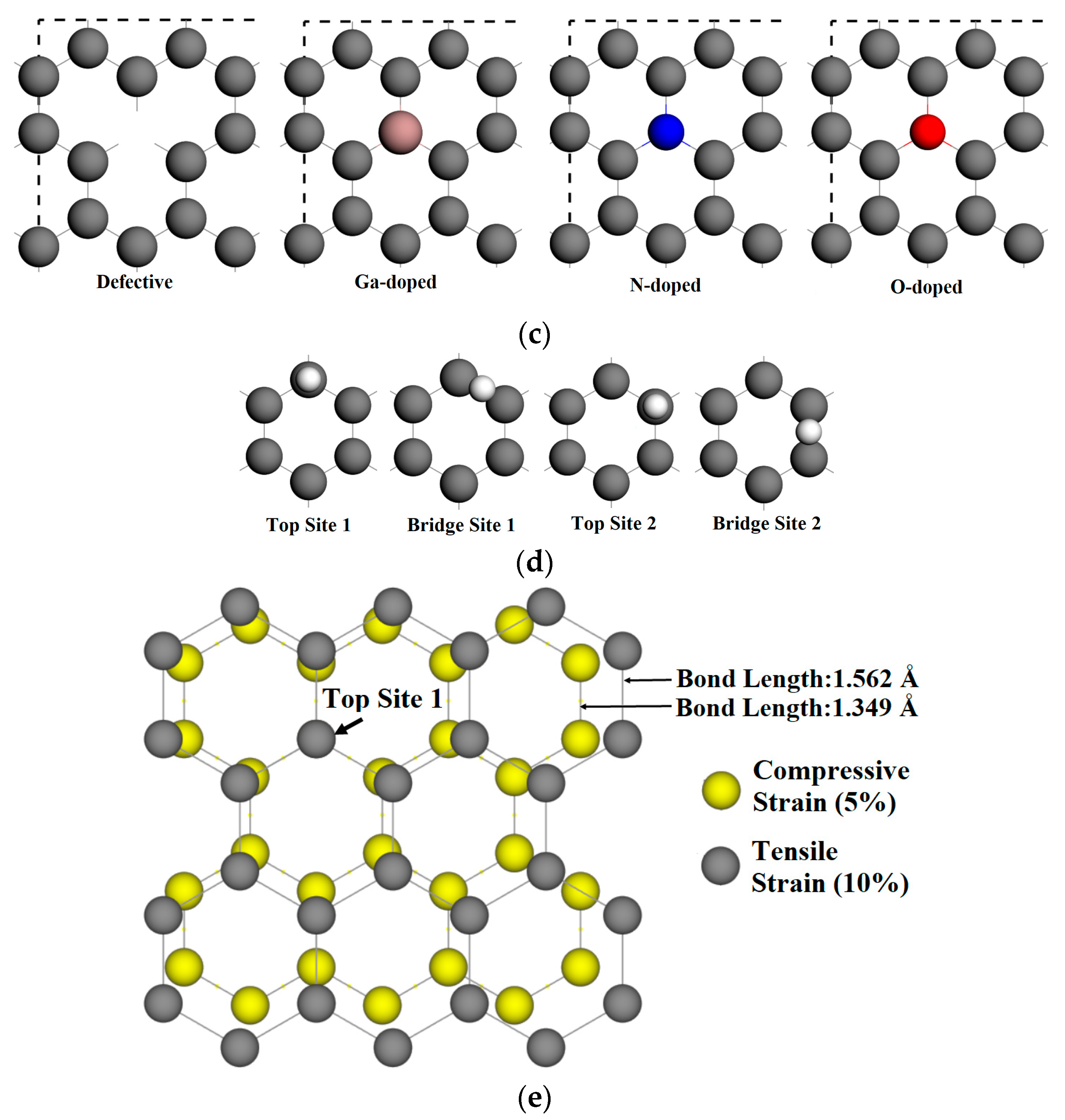
Different graphene surfaces were considered to evaluate the influence of defects and doping on adsorption. The vacancy-defected graphene structure was created by removing a carbon atom from the pristine graphene. A single carbon atom was replaced by one dopant atom to denote a doped graphene substrate. We considered three different dopant atoms: gallium, nitrogen, and oxygen. The schematics of the initial graphene sheet, a single vacancy-defected graphene surface, and a doped graphene surface are shown in Figure 1c. Considering the crystallographic symmetry of graphene, two adjacent top sites and two adjacent bridge sites were considered for comparison. Figure 1d identifies four sites for adatom adsorption on graphene, where Top Site 1 is just above the vacancy or doped atom. The adsorption distance is defined as the nearest distance between the adsorbed atom and graphene surface plane. On each adsorption site, the adsorption distance of adatoms above the graphene surface varied between 1.2 to 3 angstroms. Energy optimizations were performed for different adsorption sites and substrates. In this model, the internal stress was built in the initial doped graphene structure to evaluate the relationship of adsorption energy and adsorption distance on different graphene surfaces.
The adsorption energy Eadsorb of an adsorbed atom on graphene surface is defined as follows [32]:
where Etotal is the total energy of the graphene surface with the adsorbed atom, Esurface stands for the total energy of the graphene surface without the adsorbed atom, and Eadatom is the total energy of the adsorbed atom.
Eadsorb = Etotal − Eadatom − Esurface
Strain is introduced in graphene by changing the initial equilibrium lattice constant of graphene by a small percentage in the direction parallel to the surface. The compressive and tensile strains are applied along both the armchair and zigzag directions. The deformation of graphene substrate is represented by the strain equation:
where L and L0 are the deformed and initial equilibrium lattice constants along the x and y directions of the graphene monolayer surface (as shown in Figure 1a), respectively. In this study, S varied from −5% to 10%.
S = (L − L0)/L0
3. Results and Discussion
3.1. Adsorption on Unstrained Pristine and Vacancy-Defected Graphene
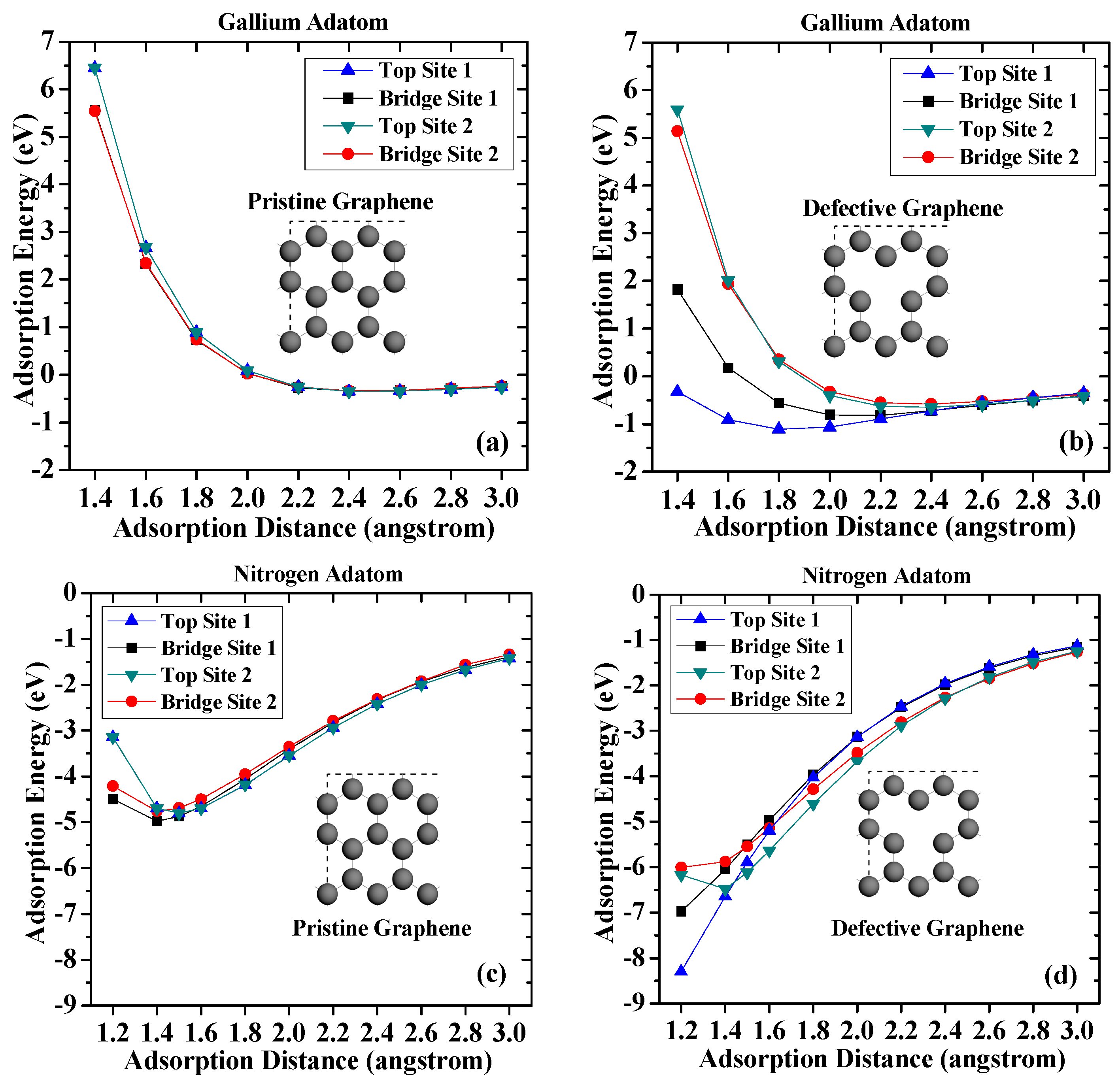
First, the adsorptions of the gallium and nitrogen adatoms on pristine and vacancy-defected graphene surfaces without strain are discussed. The results are presented in Figure 2. On the pristine graphene surface, it is found that the adsorption energies of the gallium atoms on different sites are very small. The largest adsorption energy occurs when the gallium atom adsorbed on Top Site 1. The adsorption energy is −0.349 eV and the adsorption distance is 2.4 angstrom, which indicates a weak interaction between the gallium adatom and the pristine graphene. For the vacancy-defected graphene case, it is obvious that the defect core (Top Site 1) induces a more stable interaction with the gallium adatom, followed by the defect neighbor (Bridge Site 1) and by more remote sites (Top Site 2 and Bridge Site 2). The adsorption energy for the gallium atom on Top Site 1 is −1.106 eV, which is three times that on pristine graphene. The larger adsorption energy suggests the vacancy-defected graphene exhibits a higher stability to interact with gallium adatoms than pristine graphene does.
Compared with the results for the gallium adatoms, the adsorption of nitrogen atoms on graphene exhibits a greater stability. The highest adsorption energy of nitrogen adatom on pristine graphene is −4.97 eV on Bridge Site 1, while corresponding adsorption distance is 1.4 angstrom. The adsorption energy of nitrogen adatom on top sites is slightly smaller (−4.69 eV) than those on bridge sites. There is also a slight difference of the adsorption energies on Bridge Site 1 and Bridge Site 2, which results from different C–C bonds. The larger adsorption energies and shorter distances suggest that the chemical bond is more likely to be formed between nitrogen atoms and pristine graphene surface.
The calculation results also suggest that atomic nitrogen can interact more strongly with a defective graphene surface. Among the four adsorption sites considered, Top Site 1 shows the strongest affinity to the underlying vacancy defect core. The adsorption energy dramatically increases as the adsorption distance decreases. The adsorption energy can reach −8.29 eV when the adsorption distance is 1.2 angstrom, which is nearly twice that on pristine graphene. The adsorption energies of nitrogen adatom on defective graphene on Top Site 1 and Bridge Site 1 are larger than that of Top Site 2 and Bridge Site 2, suggesting that nitrogen atoms prefer to form chemical bonds with carbon atoms around the vacancy defect. In general, the results suggest that the vacancy defect enhances adsorption stability of adatoms on defective graphene, which can be attributed to the broken π-bond around the vacancies, which induce unpaired electrons [33].
3.2. Adsorption on Doped Graphene
In this section, the adsorption behaviors of GaN on doped graphene surfaces are discussed. Figure 3 shows the adsorption energies of adatoms after graphene is doped with gallium, nitrogen, and oxygen, respectively. As shown in Figure 3a, the largest adsorption energy of the gallium adatom on Ga-doped graphene surface is −0.509 eV, which is only 0.16 eV (absolute value) larger than that on pristine graphene. These results can be explained by the fact that, after replacing the carbon atom, the gallium atom becomes an acceptor and thus easily interacts with the metal gallium [34,35]. As can be seen from Figure 3b, all the adsorption energies of the gallium adatom are reduced when they are adsorbed on N-doped graphene. Especially on Top Site 1, the adsorption energy is −0.126 eV, only about half of the other three adsorption sites, which indicates that the gallium atoms are more difficult to form stable adsorption on the surface after nitrogen incorporation in graphene. The reason behind this is the effect of nitrogen-based N-type doping, where the nitrogen atom in graphene acts as an electron donor and becomes more difficult to interact with the metal gallium adatom. On O-doped graphene surface, it can be seen that the adsorption energy is monotonically increased with the adsorption distance increasing when the gallium atom adsorbed over the oxygen atom. However, the adsorption energy of gallium adsorption on Top Site 1 is only −0.088 eV when adsorption distance is 3 angstroms. The most stable site for the gallium adatom on O-doped graphene is Bridge Site 2 with an adsorption energy of −0.316 eV, which is slightly less than that on pristine graphene. The results indicate that the incorporation of oxygen impurities makes it harder for the gallium atom to be adsorbed on the graphene, and even physical adsorption becomes very difficult.
The obtained adsorption energies for nitrogen adatom are depicted in Figure 4. For nitrogen adsorbed on the Ga-doped graphene case, when compared with pristine graphene case, the largest adsorption energy of nitrogen adsorption on Top Site 1 decreased from −4.804 to −3.312 eV, and the corresponding adsorption distance increased from 1.4 to 1.8 angstroms. Meanwhile, the largest adsorption energy of nitrogen adsorption on Bridge Site 1 decreased from −4.976 to −4.164 eV, and the corresponding adsorption distance increased from 1.4 to 1.6 angstroms. However, the adsorption energies of nitrogen adsorption on Top Site 2 and Bridge Site 2 increased to −5.846 eV and −5.566 eV, respectively. In the case of N-doped graphene, the maximum adsorption energy appeared in Bridge Site 2 with a shorter adsorption distance of 1.4 angstroms, which is closer than that on the Ga-doped graphene. For adsorption on Top Site 1, the largest adsorption distance moved to 1.4 angstroms, which is 0.1 angstroms closer to the graphene surface than that on pristine graphene. These results indicate that the nitrogen-doped atom led to a shorter chemical bond. The largest adsorption energies at Top Site 1 and Bridge Site 1 were greatly reduced, and the corresponding adsorption distance was also greatly increased, which shows that the incorporation of oxygen impurity greatly reduces the stable adsorption of the nitrogen atom.
In order to study the diffusion barriers on the adsorption processes, we assumed that the adatoms diffused from Top Site 1 to Bridge Site 1, then over Top Site 2, and finally to Bridge Site 2. The largest adsorption energies of the gallium and nitrogen adatoms on different sites are summarized in Figure 5.
As shown in Figure 5a, the gallium adatom had to overcome a barrier of around 0.012 eV when diffusing on pristine graphene, indicating a small surface migration barrier. The barrier of diffusion on vacancy-defected graphene was 0.322 eV, and the absolute value of the adsorption energy decreased gradually as the gallium adatom diffused from Top Site 1 to Bridge Site 2. The trends of the largest adsorption energy on the N-doped and O-doped surfaces were similar, which monotonically increased, as the barriers were 0.164 eV and 0.228 eV, respectively. The diffusion barrier of the gallium adatom on the Ga-doped graphene was 0.101 eV.
As shown in Figure 5b, the barrier of the nitrogen adatom diffused on the pristine graphene was 0.278 eV. This barrier of nitrogen increased to as high as 2.288 eV when it diffused on the vacancy-defected graphene. For nitrogen diffused on the Ga-doped graphene, the barrier was 2.534 eV, which was 1.538 eV for nitrogen diffused on N-doped graphene. However, for nitrogen diffused on O-doped graphene, the barrier was as large as 3.466 eV. Therefore, the effect of oxygen doping on the initial growth of GaN on graphene is greater than that of gallium doping and nitrogen doping. Therefore, as the main source of oxygen impurities, the water vapor in the reaction chamber had a significant influence on the morphology and quality of the epitaxial film growth.
3.3. Adsorption on Strained Graphene
We next studied the effects of strains on the absorption of gallium and nitrogen adatoms on graphene. In this section, the adsorption distance for the gallium adatom was 2 angstroms, while for nitrogen it was 1.5 angstrom. The dependence of the adsorption energy for the adatom on graphene on the applied compressive and tensile strains is summarized in Figure 6. Negative values on the abscissa represent compressive strains, while positive values indicate tensile strains.
For the gallium adatom adsorbed on different sites and different configuration surfaces, the absolute value of adsorption energy increased when the strain varied from −5% to 10%. It was found that lattice expansion led to increased stability for all adsorption sites and configuration surfaces. The strain enhanced the absorption of the adatom on graphene can be understood by the fact that the tensile strain generally weakens the sp2 bonding between carbon atoms. Therefore, it increases the chemical reactivity of graphene, resulting in a stronger absorption of adatoms on graphene [21,36]. From these figures, we can see that, regardless of the magnitudes of the strain, the vacancy-defected graphene was always the most stable absorption surface, for which the absorption energy was significantly lower than the pristine and doped graphene surfaces. The strain curve of Ga-doped was slightly curved at Top Site 1. For the case of nitrogen adsorption under strains, the influence of defects and doped atoms on the adsorption of nitrogen atoms were quite different. The Ga-doped graphene configuration shows that there was a nonlinear relationship as a function of strain on the Ga-doped surface. The tensile strain was found to greatly decrease the absolute value of adsorption energy of the nitrogen atom on Top Site 1, suggesting that the adsorption of the nitrogen atom above the Ga-doped atom was unlikely to happen under a larger tensile strain. The adsorption energy of nitrogen adsorption on the Ga-doped surface was very close to that of the O-doped surface when the tensile strain reached 10%, which indicates that a similar adsorption influence of that graphene under large stretching. In addition, we found that the relationship between adsorption energy and strain on vacancy-defected graphene was slightly curved. The adsorption energy of the nitrogen adatom at Bridge Site 1 on the Ga-doped graphene was larger than that on the N-doped graphene surface when there was no strain. The relationship between the adsorption energy and the strain at Bridge Site 1 on the Ga-doped graphene was still non-linear. As the tensile strain increased, the adsorption energy of the nitrogen adatom on the Ga-doped graphene increased slightly and then decreased gradually. When the tensile strain reached 10%, the adsorption energy of the nitrogen adatom on the Ga-doped graphene was 0.26 eV less than that on the N-doped graphene. The difference in adsorption energy between the vacancy-defected substrate and the pristine graphene decreased gradually under compressive strain, and gradually increased under tensile strain. It can be seen that the difference in adsorption energies at Top Site 2 between the O-doped graphene and the N-doped graphene was small under low strain, which increased greatly under a large tensile strain. Due to the fact that adsorbed atoms were far away from the defect core and the doped atom, the strain dependences of the adsorption energy of the adsorbed atom at Bridge Site 2 were much closer.
Furthermore, a nearly linear relationship between the strains and adsorption energies can be observed in Figure 6. It is necessary to further understand the impact of strain on adsorption on different sites. By a linear fitting of the calculation results, the in-plane strain dependence of the adsorption energy can be expressed as
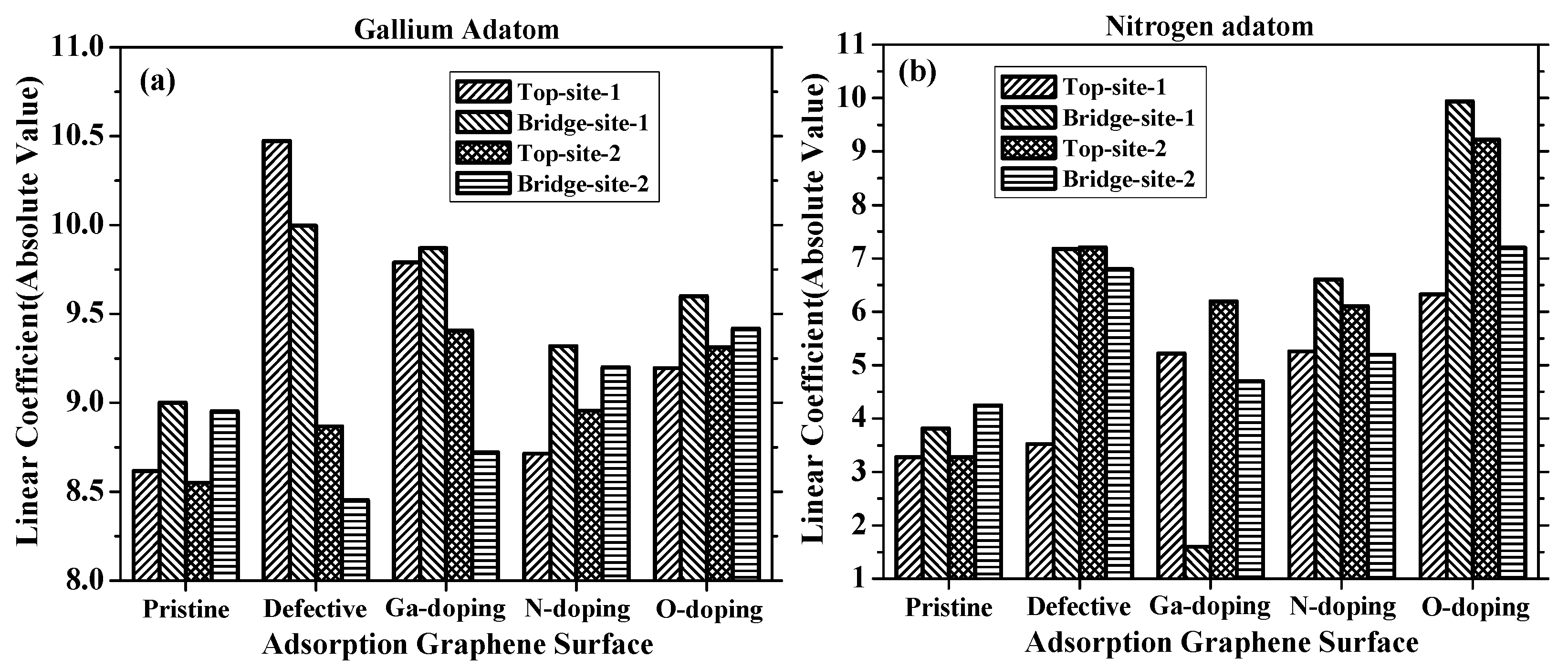
where S represents the change in lattice parameters along the strain plane, as described in Equation (2), A is the linear coefficient characterizing the relationship between the adsorption energies and strains. The strain in correspondence to the absolute value of the linear coefficient is summarized in Figure 7.
Ea = E0 + A × S
For adsorption on the pristine graphene, both for gallium and nitrogen, it was found that the linear coefficient at the bridge sites were larger than that at the top sites, indicating that the adatoms on the bridge sites were more sensitive with strains than that on the top sites. This was due to the fact that the adatom at the bridge sites was closer to the surrounding moving carbon atoms and thus had a greater impact on strain. In addition, the coefficients of the gallium adsorbed on the pristine graphene were more than twice as high as those of nitrogen, indicating that the strains had a greater impact on gallium adatom adsorptions.
For adsorption on the vacancy-defected graphene, it was found that the coefficient of the gallium at Top Site 1 was larger than that at other sites. The coefficient decreased, while the gallium adatom diffused along the path mentioned above. On the contrary, the coefficient of nitrogen at Top Site 1 was smaller than that at other sites. The largest absolute value of linear coefficient resulted from the fact that, under tensile strain, the absorption energy of gallium over the vacancy defect core increased more significantly than that over carbon and doped atoms. However, the coefficient of nitrogen adsorbed on Top Site 1 was much lower than those on other sites, which indicates an insensitive adsorption on strains.
For Ga-doped graphene, due to the strong nonlinear relationship, the linear coefficient of fitting could only be used as an approximate reference. The coefficients of the gallium adatom on Top Site 1 and Bridge Site 1 were similar, and they were larger than those of Top Site 2 and Bridge Site 2. The coefficient of nitrogen on Top Site 1 was positive in value, while the others were negative in value, showing the different impact trend of nitrogen adsorption on Ga-doped graphene. The coefficients of nitrogen adsorption on the O-doped graphene were larger than those on the N-doped graphene at each site. The largest coefficient of nitrogen adsorption was present at Bridge Site 1 for both N-doped and O-doped graphene, whereas the lowest coefficient was present at Top Site 1. In the gallium adatom case, the adsorption on N-doped and O-doped graphene showed similar variation to that on pristine graphene, which means that the coefficients at the bridge sites were larger than those at the top sites. However, the coefficients of nitrogen adsorption on N-doped and O-doped graphene surface show that strain has greater impact on nitrogen adatom at Top Site 2 than that at Bridge Site 2.
4. Conclusions
In summary, we investigated gallium and nitrogen adsorption on vacancy-defected and doped graphene. A weak interaction was found between the gallium adatom and the pristine graphene, whereas the adsorption of the nitrogen atom on graphene exhibited greater stability. The vacancy defect core enhanced the adsorption stability of adatoms on graphene, whereas the incorporation of oxygen impurity greatly reduced the stable adsorption of gallium and nitrogen adatoms. Furthermore, the strain effects on adsorption on graphene were studied. The lattice expansion led to increased stability for all adsorption sites and configuration surfaces, except for nitrogen adsorption over the gallium atom in the Ga-doped graphene. The study presented in this paper may have important implications in understanding GaN growth on graphene.
Acknowledgments
This work was supported by the grants from the National Natural Science Foundation of China (No. 51402224). It was also supported by the National Natural Science Foundation of China (No. 51727901), the Major State Basic Research Development Program of China (973 Program), with the contract number of 2011CB013103, and the State Scholarship Fund of China (No. 201606955052).
Author Contributions
Han Yan performed the calculations and wrote the paper; Zhi-Yin Gan and Sheng Liu conceived and coordinated the scientific work and made corrections to the English; Pei-Cheng Ku and Peng Li made comments and revised the manuscript.
Conflicts of Interest
The authors declare no conflict of interest.
References
- Novoselov, K.S.; Geim, A.K.; Morozov, S.V.; Jiang, D.; Zhang, Y.; Dubonos, S.V.; Grigorieva, I.V.; Firsov, A.A. Electric field effect in atomically thin carbon films. Science 2004, 306, 666–669. [Google Scholar] [CrossRef] [PubMed]
- Chung, K.; Lee, C.-H.; Yi, G.-C. Transferable GaN layers grown on ZnO-coated graphene layers for optoelectronic devices. Science 2010, 330, 655–657. [Google Scholar] [CrossRef] [PubMed]
- Zhou, S.; Liu, X. Effect of v-pits embedded InGaN/GaN superlattices on optical and electrical properties of GaN-based green light-emitting diodes. Phys. Status Solidi (A) 2017, 214. [Google Scholar] [CrossRef]
- Agata, B.; Grzegorz, M.; Czesław, S.; Ewa, G.; Przemysław, W.; Irina, M.; Robert, C.; Tadek, S.; Piotr, P. Influence of the growth method on degradation of InGaN laser diodes. Appl. Phys. Express 2017, 10, 091001. [Google Scholar]
- Cheng, Z.; Zhao, Z.; Ke, H.; Liu, G.; Dong, Z.; Gao, S. High efficiency broadband GaN HEMT power amplifier based on three-frequency point matching method. Microw. Opt. Technol. Lett. 2017, 59, 1850–1855. [Google Scholar] [CrossRef]
- Hu, H.; Zhou, S.; Liu, X.; Gao, Y.; Gui, C.; Liu, S. Effects of GaN/AlGaN/sputtered AlN nucleation layers on performance of GaN-based ultraviolet light-emitting diodes. Sci. Rep. 2017, 7, 44627. [Google Scholar] [CrossRef] [PubMed]
- Al Balushi, Z.Y.; Miyagi, T.; Lin, Y.-C.; Wang, K.; Calderin, L.; Bhimanapati, G.; Redwing, J.M.; Robinson, J.A. The impact of graphene properties on GaN and AlN nucleation. Surf. Sci. 2015, 634, 81–88. [Google Scholar] [CrossRef]
- Kumaresan, V.; Largeau, L.; Madouri, A.; Glas, F.; Zhang, H.; Oehler, F.; Cavanna, A.; Babichev, A.; Travers, L.; Gogneau, N.; et al. Epitaxy of GaN nanowires on graphene. Nano Lett. 2016, 16, 4895–4902. [Google Scholar] [CrossRef] [PubMed]
- Kim, J.; Bayram, C.; Park, H.; Cheng, C.-W.; Dimitrakopoulos, C.; Ott, J.A.; Reuter, K.B.; Bedell, S.W.; Sadana, D.K. Principle of direct van der Waals epitaxy of single-crystalline films on epitaxial graphene. Nat. Commun. 2014, 5, 4836. [Google Scholar] [CrossRef] [PubMed]
- Lee, C.-H.; Kim, Y.-J.; Hong, Y.J.; Jeon, S.-R.; Bae, S.; Hong, B.H.; Yi, G.-C. Flexible inorganic nanostructure light-emitting diodes fabricated on graphene films. Adv. Mater. 2011, 23, 4614–4619. [Google Scholar] [CrossRef] [PubMed]
- Chung, K.; Beak, H.; Tchoe, Y.; Oh, H.; Yoo, H.; Kim, M.; Yi, G.-C. Growth and characterizations of GaN micro-rods on graphene films for flexible light emitting diodes. APL Mater. 2014, 2, 092512. [Google Scholar] [CrossRef]
- Gupta, P.; Rahman, A.A.; Hatui, N.; Gokhale, M.R.; Deshmukh, M.M.; Bhattacharya, A. Movpe growth of semipolar III-nitride semiconductors on CVD graphene. J. Cryst. Growth 2013, 372, 105–108. [Google Scholar] [CrossRef]
- Ohta, J.; Shon, J.W.; Ueno, K.; Kobayashi, A.; Fujioka, H. Gan-based light-emitting diodes with graphene buffers for their application to large-area flexible devices. IEICE Trans. Electron. 2017, E100.C, 161–165. [Google Scholar] [CrossRef]
- Shunyu, H.; Yu, X.; Lin, Q.; Zongyao, L.; Bing, C.; Chinhua, W.; Jicai, Z.; Jianfeng, W.; Ke, X. Growth of low-threading-dislocation-density GaN on graphene by hydride vapor phase epitaxy. Jpn. J. Appl. Phys. 2017, 56, 030308. [Google Scholar]
- Hwang, S.W.; Choi, S.-H. Successful fabrication of GaN epitaxial layer on non-catalytically-grown graphene. Bull. Korean Chem. Soc. 2016, 37, 1004–1009. [Google Scholar] [CrossRef]
- Heilmann, M.; Munshi, A.M.; Sarau, G.; Göbelt, M.; Tessarek, C.; Fauske, V.T.; van Helvoort, A.T.J.; Yang, J.; Latzel, M.; Hoffmann, B.; et al. Vertically oriented growth of GaN nanorods on Si using graphene as an atomically thin buffer layer. Nano Lett. 2016, 16, 3524–3532. [Google Scholar] [CrossRef] [PubMed]
- Wang, X.; Sun, G.; Routh, P.; Kim, D.-H.; Huang, W.; Chen, P. Heteroatom-doped graphene materials: Syntheses, properties and applications. Chem. Soc. Rev. 2014, 43, 7067–7098. [Google Scholar] [CrossRef] [PubMed]
- Goncalves, G.; Marques, P.A.A.P.; Granadeiro, C.M.; Nogueira, H.I.S.; Singh, M.K.; Grácio, J. Surface modification of graphene nanosheets with gold nanoparticles: The role of oxygen moieties at graphene surface on gold nucleation and growth. Chem. Mater. 2009, 21, 4796–4802. [Google Scholar] [CrossRef]
- Jin, N.; Han, J.; Wang, H.; Zhu, X.; Ge, Q. A DFT study of oxygen reduction reaction mechanism over O-doped graphene-supported Pt4, Pt3Fe and Pt3V alloy catalysts. Int. J. Hydrogen Energy 2015, 40, 5126–5134. [Google Scholar] [CrossRef]
- Guinea, F.; Katsnelson, M.I.; Geim, A.K. Energy gaps and a zero-field quantum hall effect in graphene by strain engineering. Nat. Phys. 2009, 6, 30–33. [Google Scholar] [CrossRef]
- Yang, M.; Nurbawono, A.; Zhang, C.; Wu, R.; Feng, Y.; Ariando. Manipulating absorption and diffusion of H atom on graphene by mechanical strain. AIP Adv. 2011, 1, 032109. [Google Scholar] [CrossRef]
- Car, R.; Parrinello, M. Unified approach for molecular dynamics and density-functional theory. Phys. Rev. Lett. 1985, 55, 2471–2474. [Google Scholar] [CrossRef] [PubMed]
- Wlazło, M.; Majewski, J. First principles study of gas adsorption dynamics on pristine and defected graphene. Acta Phys. Pol. A 2016, 129. [Google Scholar] [CrossRef]
- Yan, H.; Gan, Z.; Song, X.; Lv, Q.; Xu, J.; Liu, S. Car–Parrinello simulation of initial growth stage of gallium nitride on carbon nanotubes. Phys. E Low-Dimens. Syst. Nanostruct. 2009, 41, 1143–1146. [Google Scholar] [CrossRef]
- Goedecker, S.; Teter, M.; Hutter, J. Separable dual-space gaussian pseudopotentials. Phys. Rev. B 1996, 54, 1703–1710. [Google Scholar] [CrossRef]
- Bungaro, C.; Rapcewicz, K.; Bernholc, J. Ab initio phonon dispersions of wurtzite AlN, GaN, and InN. Phys. Rev. B 2000, 61, 6720–6725. [Google Scholar] [CrossRef]
- Becke, A.D. Density-functional exchange-energy approximation with correct asymptotic behavior. Phys. Rev. A 1988, 38, 3098–3100. [Google Scholar] [CrossRef]
- Lee, C.; Yang, W.; Parr, R.G. Development of the Colle-Salvetti correlation-energy formula into a functional of the electron density. Phys. Rev. B 1988, 37, 785–789. [Google Scholar] [CrossRef]
- Perdew, J.P.; Zunger, A. Self-interaction correction to density-functional approximations for many-electron systems. Phys. Rev. B 1981, 23, 5048–5079. [Google Scholar] [CrossRef]
- Krasheninnikov, A.V.; Lehtinen, P.O.; Foster, A.S.; Nieminen, R.M. Bending the rules: Contrasting vacancy energetics and migration in graphite and carbon nanotubes. Chem. Phys. Lett. 2006, 418, 132–136. [Google Scholar] [CrossRef]
- Cooper, D.R.; D’Anjou, B.; Ghattamaneni, N.; Harack, B.; Hilke, M.; Horth, A.; Majlis, N.; Massicotte, M.; Vandsburger, L.; Whiteway, E. Experimental review of graphene. ISRN Condens. Matter Phys. 2012, 2012, 501686. [Google Scholar] [CrossRef]
- Rad, A.S. First principles study of Al-doped graphene as nanostructure adsorbent for NO2 and N2O: DFT calculations. Appl. Surf. Sci. 2015, 357, 1217–1224. [Google Scholar] [CrossRef]
- Zhou, Q.; Ju, W.; Su, X.; Yong, Y.; Li, X. Adsorption behavior of SO2 on vacancy-defected graphene: A DFT study. J. Phys. Chem. Solids 2017, 109, 40–45. [Google Scholar] [CrossRef]
- Huang, L.F.; Ni, M.Y.; Zhang, G.R.; Zhou, W.H.; Li, Y.G.; Zheng, X.H.; Zeng, Z. Modulation of the thermodynamic, kinetic, and magnetic properties of the hydrogen monomer on graphene by charge doping. J. Chem. Phys. 2011, 135, 064705. [Google Scholar] [CrossRef] [PubMed]
- Losurdo, M.; Yi, C.; Suvorova, A.; Rubanov, S.; Kim, T.-H.; Giangregorio, M.M.; Jiao, W.; Bergmair, I.; Bruno, G.; Brown, A.S. Demonstrating the capability of the high-performance plasmonic gallium–graphene couple. ACS Nano 2014, 8, 3031–3041. [Google Scholar] [CrossRef] [PubMed]
- Xu, Y.; Mavrikakis, M. Adsorption and dissociation of O2 on gold surfaces: Effect of steps and strain. J. Phys. Chem. B 2003, 107, 9298–9307. [Google Scholar] [CrossRef]
Figure 1.
The top view and side view of calculation model. (a) 3 × 2 of the represented pristine graphene surface; (b) Monolayer graphene substrates and vacuum layer; (c) Vacancy-defected and doped graphene surfaces, where the dangling bonds are presented in the vacancy-defected graphene surface; (d) Four adsorption sites for atomic gallium and nitrogen on graphene, where Top Site 1 is just above the vacancy or doped atom; (e) The structure of strained graphene in the two limit cases.


Figure 2.
Adsorption energy curves of (a) the gallium adatom on pristine graphene; (b) the gallium atom on vacancy-defected graphene; (c) the nitrogen atom on pristine graphene; and (d) the nitrogen atom on vacancy-defected graphene.
Figure 2.
Adsorption energy curves of (a) the gallium adatom on pristine graphene; (b) the gallium atom on vacancy-defected graphene; (c) the nitrogen atom on pristine graphene; and (d) the nitrogen atom on vacancy-defected graphene.

Figure 3.
Adsorption energies of gallium on (a) Ga-doped graphene; (b) N-doped graphene; (c) O-doped graphene.
Figure 3.
Adsorption energies of gallium on (a) Ga-doped graphene; (b) N-doped graphene; (c) O-doped graphene.
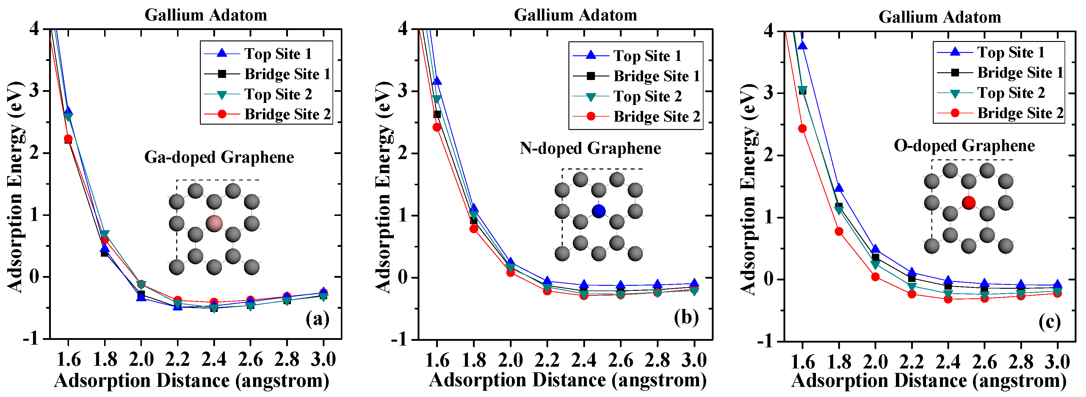
Figure 4.
Adsorption energies of nitrogen on (a) Ga-doped graphene; (b) N-doped graphene; and (c) O-doped graphene.
Figure 4.
Adsorption energies of nitrogen on (a) Ga-doped graphene; (b) N-doped graphene; and (c) O-doped graphene.
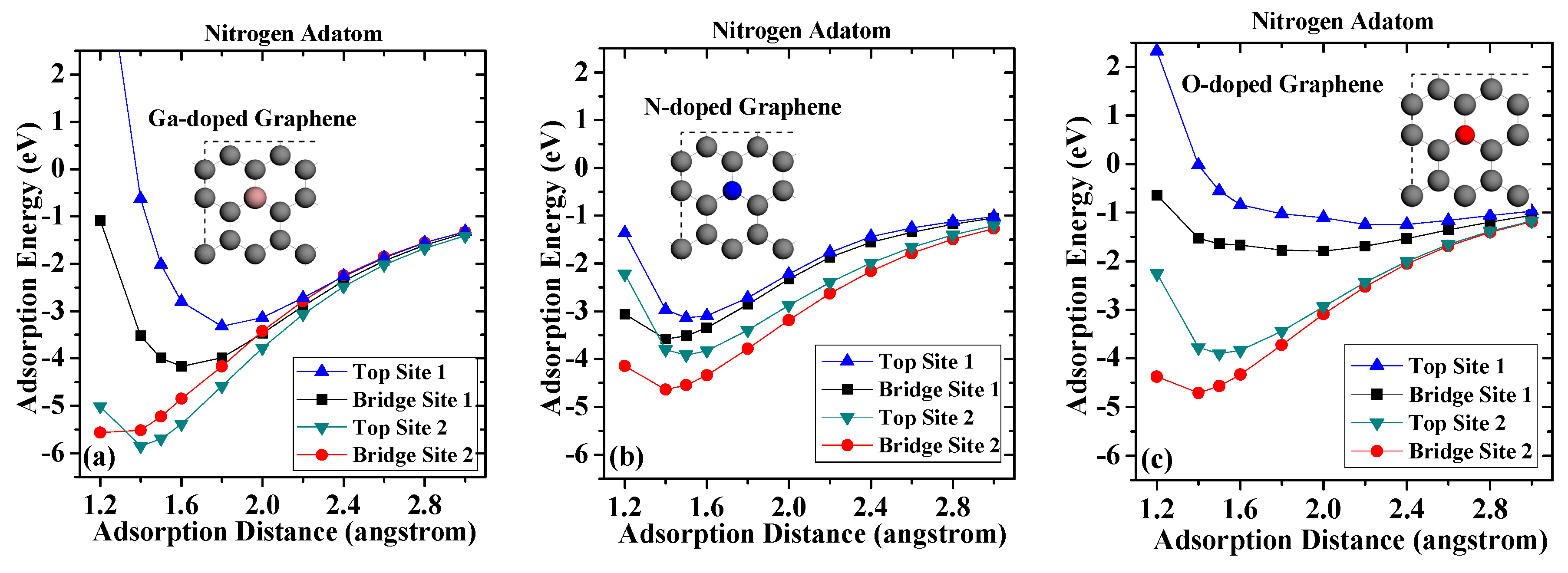
Figure 5.
The values for the diffusion barriers of the (a) gallium and (b) nitrogen adatoms.
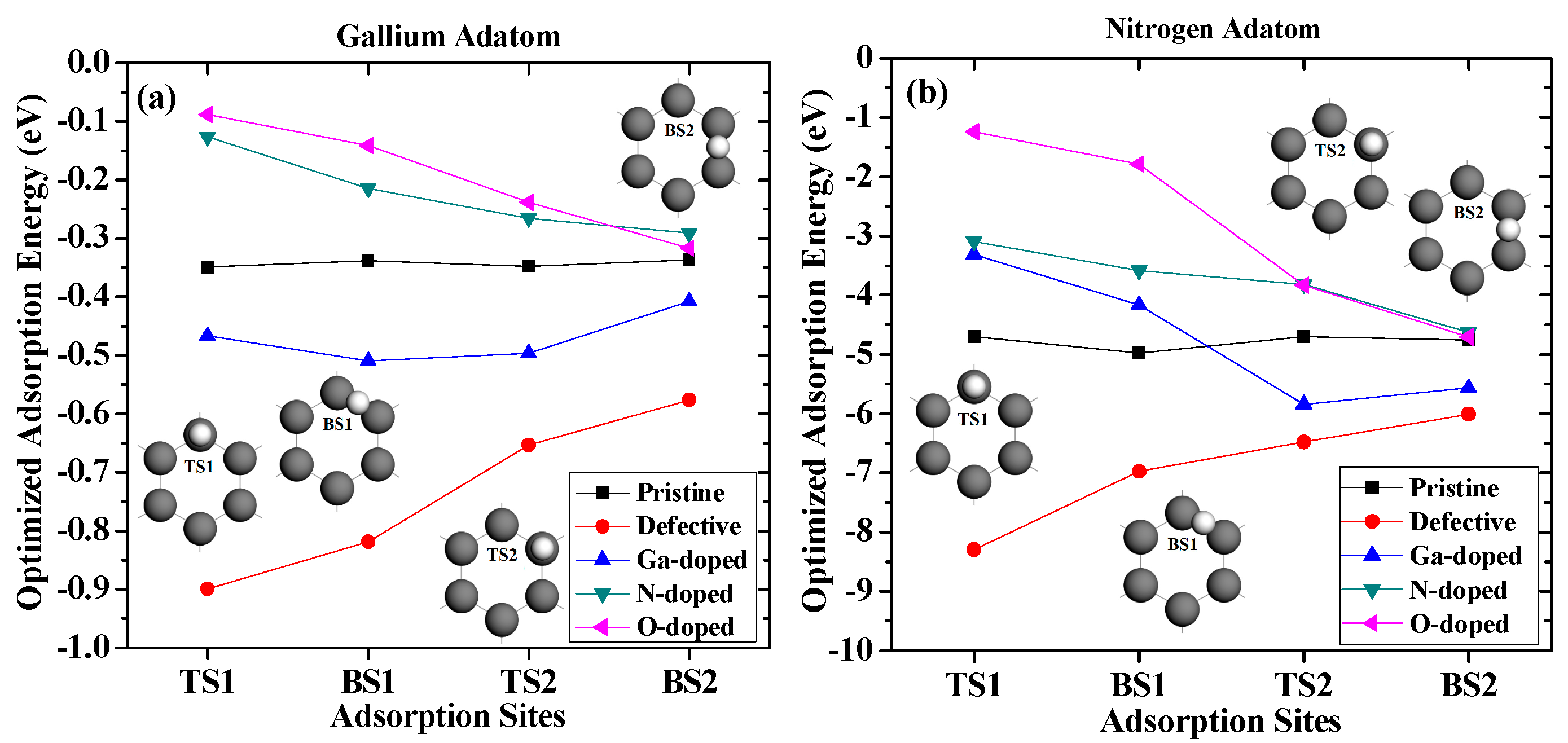
Figure 6.
The dependence of adsorption energy for gallium adatom adsorption on graphene at (a) Top Site 1; (b) Bridge Site 1; (c) Top Site 2; (d) Bridge Site 2; and nitrogen adatom adsorption on graphene at (e) Top Site 1; (f) Bridge Site 1; (g) Top Site 2; (h) Bridge Site 2e on the applied compressive and tensile strain, respectively.
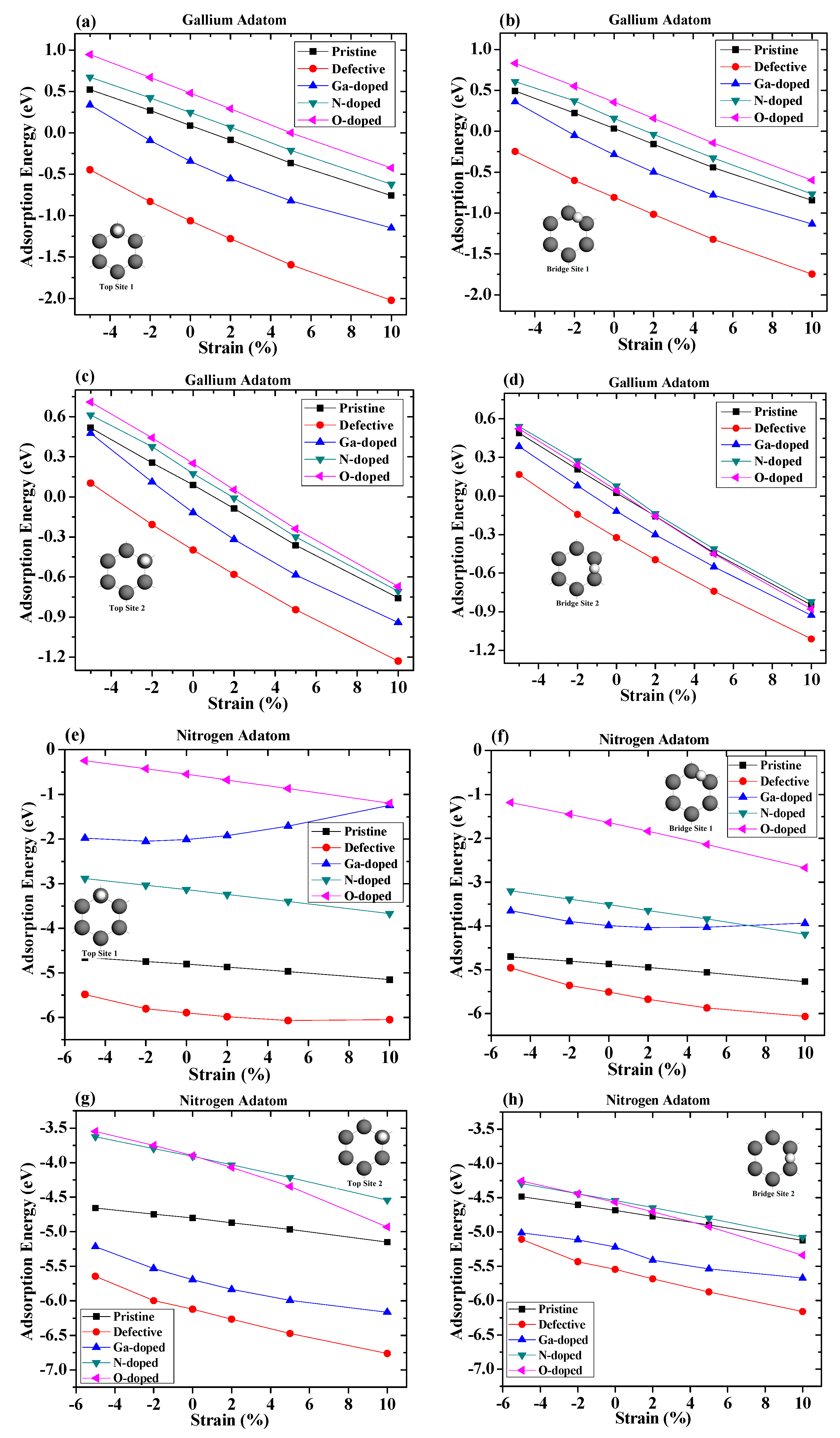
Figure 7.
Absolute value of linear coefficient characterizing the relationship between the adsorption energies and strains for (a) gallium adatom and (b) nitrogen adatom.
Figure 7.
Absolute value of linear coefficient characterizing the relationship between the adsorption energies and strains for (a) gallium adatom and (b) nitrogen adatom.

© 2018 by the authors. Licensee MDPI, Basel, Switzerland. This article is an open access article distributed under the terms and conditions of the Creative Commons Attribution (CC BY) license (http://creativecommons.org/licenses/by/4.0/).
Share and Cite
MDPI and ACS Style
Yan, H.; Ku, P.-C.; Gan, Z.-Y.; Liu, S.; Li, P. Strain Effects in Gallium Nitride Adsorption on Defective and Doped Graphene: First-Principles Calculations. Crystals 2018, 8, 58. https://doi.org/10.3390/cryst8020058
AMA Style
Yan H, Ku P-C, Gan Z-Y, Liu S, Li P. Strain Effects in Gallium Nitride Adsorption on Defective and Doped Graphene: First-Principles Calculations. Crystals. 2018; 8(2):58. https://doi.org/10.3390/cryst8020058
Chicago/Turabian StyleYan, Han, Pei-Cheng Ku, Zhi-Yin Gan, Sheng Liu, and Peng Li. 2018. "Strain Effects in Gallium Nitride Adsorption on Defective and Doped Graphene: First-Principles Calculations" Crystals 8, no. 2: 58. https://doi.org/10.3390/cryst8020058
Note that from the first issue of 2016, this journal uses article numbers instead of page numbers. See further details here.