
Graphene Coated Nanoprobes: A Review

Institute of Functional Nano& Soft Materials, Collaborative Innovation Center of Suzhou Nano Science and Technology, Soochow University, Suzhou 215123, China
*
Author to whom correspondence should be addressed.
Crystals 2017, 7(9), 269; https://doi.org/10.3390/cryst7090269
Submission received: 25 July 2017
/
Revised: 24 August 2017
/
Accepted: 28 August 2017
/
Published: 8 September 2017
(This article belongs to the Special Issue Integration of 2D Materials for Electronics Applications)
Abstract
:Nanoprobes are one of the most important components in several fields of nanoscience to study materials, molecules and particles. In scanning probe microscopes, the nanoprobes consist on silicon tips coated with thin metallic films to provide additional properties, such as conductivity. However, if the experiments involve high currents or lateral frictions, the initial properties of the tips can wear out very fast. One possible solution is the use of hard coatings, such as diamond, or making the entire tip out of a precious material (platinum or diamond). However, this strategy is more expensive and the diamond coatings can damage the samples. In this context, the use of graphene as a protective coating for nanoprobes has attracted considerable interest. Here we review the main literature in this field, and discuss the fabrication, performance and scalability of nanoprobes.
1. Introduction
Sharp probe tips with an apex radius <100 nm are widely used in many different fields of science including electronics [1], physics [2], chemistry [3], biology [4] and medicine [5], as they allow local characterization and manipulation of materials with a nanometric spatial resolution. Depending on the equipment and application in which they are used, nanoprobes can have a wide variety of shapes, material composition and prizes. One of the main problems of nanoprobes is that they can lose their initial properties (e.g., sharpness, conductivity) after several experiments, leading to false data collection and increases in the cost of the research (i.e., new probes need to be used). Therefore, understanding the degradation process and the speed of nanoprobes during each experiment is essential to ensure high quality, reliable and cheap data collection.
Scanning Probe Microscopes (SPM) are among the most advanced equipments for nanoscale characterization and patterning, as they can achieve high spatial resolution both laterally (<0.1 nm) and vertically (<0.01 nm) [6,7]. The nanoprobes used in SPMs consist of a cantilever with a sharp tip at its end, which is the only part that contacts the sample being tested. The lateral resolution of the data collected with an SPM in most cases depends on the sharpness of the nanoprobe at its apex: the smaller the tip radius, the smaller the tip–sample contact area, and therefore the higher the lateral resolution [6]. When using an SPM to analyze the morphological properties of a material (e.g., topography, adhesion force) normally Si or Si3N4 nanoprobes are used, as they can be easily fabricated by standard silicon bulk micromachining technology [8]. The tip radius at the tip apex can be as small as ~2 nm. For electrical modes of SPMs, such as conductive atomic force microscopy (C-AFM), electrical force microscopy (EFM) and Kelvin probe force microscopy (KPFM), the probes need to be conductive, a capability that can be provided by coating the Si or Si3N4 nanoprobes with a thin (~20 nm) conductive varnish [9]. The conductive varnish (normally a metal or doped diamond) should be thick enough to provide stable conductivity to the tips under high current densities and frictions, and at the same time thin enough for not increasing the radius at the apex too much (this would result in a loss of lateral resolution). Maintaining the initially high conductivity and sharpness of conductive nanoprobes during several experiments is one of the main problems for the users of electrical modes of SPMs [10]. It is worth noting that the contact area between the tip of an SPM and the sample is typically <100 nm2, and that the minimum current that this equipment can measure is ~1pA. Therefore, the minimum current that an SPM can detect is 1 A/cm2. This is already a very high current density, but it can go even higher, up to 109 A/cm2 if the currents detected with the SPM increase into the milliampere regime [11]. According to the International Technology Roadmap of Semiconductors [12], sub-10 nm resolution and a dynamic range of 1016–1020 A/cm2 is required to acquire electrical information in future nanoscale devices [13,14].
In the market place, one can also find conductive nanoprobes for SPMs made of solid metals or doped diamond. However, these nanoprobes show many disadvantages: (i) much higher cost (up to 10-times) due to the use of precious materials and hone techniques; (ii) very few suppliers and a very limited range of spring constants, resonance frequencies and tip radiuses; and (iii) damage to the samples due to high stiffness (for the diamond tips), which not only produces degradation of the sample under test, but also abundant adhesion of particles to the tip apex and subsequent reduction of its sharpness and conductivity. Table 1 summarizes the most used conductive nanoprobes for SPMs, and classifies them into four categories depending on their material structure: metal varnished Si probes, doped diamond varnished Si probes, solid metallic probes and solid doped diamond probes. Despite the wide range of conductive nanoprobes available in the market, currently none of them possess high spatial resolution, high conductivity, long durability and low cost at the same time. Therefore the exploration of novel materials with high conductivity and wear resistance is necessary to promote nanoscale characterization techniques.
Researchers have been working on designing prototypes of nanoprobes coated with specific materials. For example, Dai et al. [15] modified conventional SPM probe tips by attaching multiple walled carbon nanotubes (diameter of 5–20 nm and length of 1 μm) to their apex using epoxy and manual manipulation under optical microscope. Afterwards, the attachment method was improved with the assistance of DC current flow [16]. Tay et al. [17] attached single metallic (tungsten or cobalt) nanowires to commercial AFM tips, and successfully used them to profile a steep sidewall structure with high resolution due to their tiny radius of curvature (1–2 nm) and high aspect ratio (length of ~100 nm, height of ~1.5 μm). Bakhti et al. [18] grew a gold nano-filament with radius of <3 nm and length of 10–100 nm on the apex of conductive SPM nanoprobes, and the resulting nanoprobe was shown to be chemically inert with improved lateral resolution (observable from the topographic maps). The emergence of two dimensional (2D) materials with superior properties (mechanical strength, flexibility, transparency, thermal conductivity, chemical stability, among others) [19,20,21,22], has also been attractive in the field of conductive nanoprobes engineering. Several works [23,24,25,26,27,28,29] have demonstrated that graphene would be an ideal coating material to enhance the lifetime of a conductive nanoprobe, as it can provide high conductivity and mechanical robustness without increasing the tip radius (it is just one atom thick) and/or modifying the spring constant of the cantilever (its mass is negligible, while hard coatings like diamond have a considerable mass that bend the cantilevers and alter their mechanical and dynamic properties). Furthermore, graphene could be used to functionalize the surface of the probes, providing additional properties like hydrophobicity and piezoelectricity. In this review, we present a detailed summary of all the graphene coated nanoprobes developed, and describe several characteristics including the fabrication technologies and performances.
2. Graphene-Coated AFM Probes Production
2.1. Direct Chemical Vapor Deposition of Graphene on AFM Nanoprobes
Chemical vapor deposition (CVD) is a widespread methodology used to produce high quality, large area and continuous graphene films on the surface of different metal catalysts (e.g., Cu [30], Fe [31], Ni [32]). To do so, the metallic substrate (typically a foil) is introduced in a tube CVD furnace and heated at high temperatures (>850 °C) while the graphene precursor (typically CH4 or C2H5OH) is introduced in the tube with the assistance of a carrier gas (typically H2/Ar). Using this approach, the precursor seeds (carbon-containing molecules) can precipitate at random locations on the surface of the metallic sample, and they grow until merging into each other, forming a homogeneous (but polycrystalline) graphene film—intuitively this process is similar to placing several ice cubes on a flat table and waiting until they melt and form a homogeneous water film. By controlling the amount of precursor in the chamber, the temperature and growth time, the properties of the graphene sheets can be tuned (e.g., domain size, graphene thickness). As the growth takes place at all locations of the sample simultaneously, the growth process is scalable.
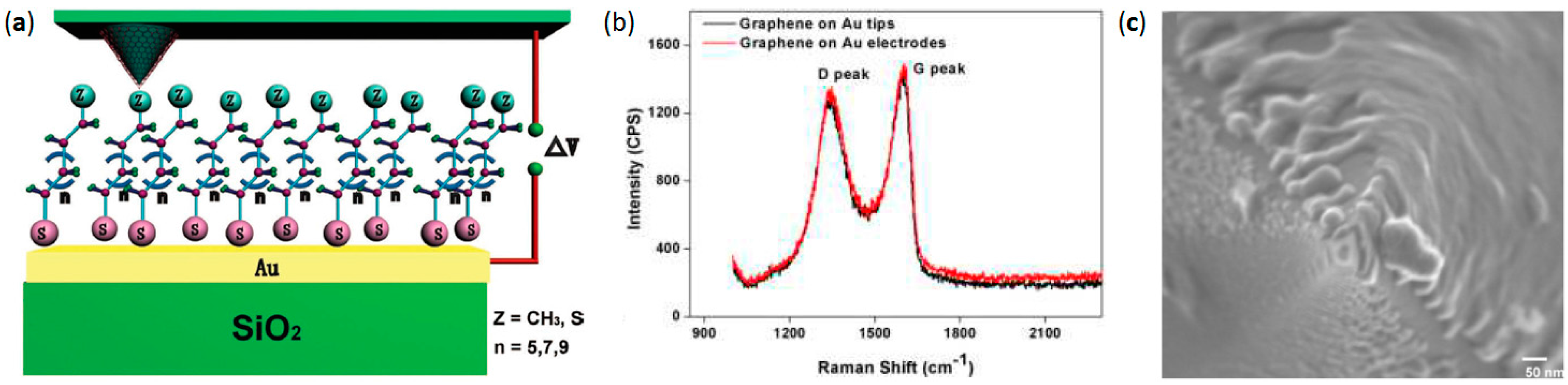
Wen et al. [23] attempted to grow graphene on the surface of Au-varnished Si nanoprobes via CVD. To do so, they inserted the nanoprobes (from Mikromash model CSC38/Cr-Au) in a tube furnace and ran the CVD process (Figure 1a). C2H5OH was used to supply the carbon source and delivered to the Au-coated nanoprobe by the mixed gases of Ar/H2 for 5 min, under a flow rate of 100 sccm at 750–850 °C. The authors claim that, as the tips are varnished with Au (which can serve as a metallic catalyst), the graphene would form on the surface of the Au and eventually cover the entire surface of the nanoprobe. In order to demonstrate the correct growth of graphene the authors compare the Raman spectra of the graphene films grown on Au electrodes and Au-varnished tips, and both showed peaks at 1597 cm−1 (Figure 1b). However, the scanning electron microscopy (SEM) images of the tip apex shown by the authors reveal the material deposited on the tip apex appears to be very un-homogenous and thick (Figure 1c), meaning that this carbon-rich material may not hold the genuine properties of 2D graphene sheets.
It should be highlighted that the growth of 2D materials on metallic substrates has been normally performed using metallic foils, not metal-varnished surfaces. The reason is that large amounts of metal need to be available on the surface of the sample to avoid massive diffusion and de-wetting at high temperatures >850 °C. Very few authors successfully achieved the CVD growth of graphene or any other 2D material on metal-varnished samples (300 nm SiO2/Si) [33,34,35], and in all cases the thickness of the metal was >500 nm. In Ref. [23], the authors used standard Au-varnished Si nanoprobes for SPMs, on which the Au-varnish is <70 nm thick. They recognized discontinuous graphene growth due to uncontrollable Au melting. Despite the authors showing that their graphene coated nanoprobes achieved enhanced performance (90% yield) as a molecular junction, to the best of our knowledge this approach has never been reproduced by these or other authors, and the graphene grown by this method contains a large number of defects, which is indicated by the strong D peak. Therefore, this is not an ideal methodology for graphene coating on the AFM tips.
2.2. Transfer of CVD-Grown Graphene onto AFM Probes
As the temperatures required for the CVD growth of graphene are very high, avoiding the use of this method directly on the tips is necessary. One of the main advantages of CVD-grown 2D materials is that they can be prepared on a substrate that ensures very high quality (e.g., Cu foils) and is then transferred onto the target device. Lanza et al. [24] coated commercially available AFM probes with a sheet of graphene previously grown on a Cu foil. During the fabrication process two samples were prepared independently and merged (see Figure 2a). Single layer graphene was synthesized via CVD approach on a 25 μm thick Cu foil, using 20 sccm methane gas mixed with 10 sccm hydrogen in a tube furnace working at a growth temperature of 1000 °C for 15 min. After that, the furnace was cooled down to room temperature under the flow rate of 10 sccm hydrogen. During this process, carbon-containing sources precipitated and eventually graphene films formed on both sides of the Cu substrate. After the growth, the graphene/Cu/graphene stack was introduced to an oxygen plasma furnace to remove one side of the graphene layers. The resulting graphene/Cu stack was fixed in a spinner and a drop of PMMA was deposited on top of the graphene sheet and spun at 1000 rpm for 1 min. Then, the sample was backed on a hot plate at 170 °C for 5 min until the PMMA became solid, resulting in an average thickness of ~200 nm. The PMMA/graphene/Cu stack was deposited on the surface of a FeCl3 solution for etching the Cu substrate. After that, the PMMA/graphene stack was fished and washed, first in a 2% HCl solution and later in deionized water. Meanwhile, a commercial PtIr-varnished silicon AFM tip was fully wrapped and glued on a cleaned piece of Si wafer. To do so, the surface of the Si was first covered with a ~200 nm layer of PMMA (spun at 1000 rpm for 1 min and baked at 170 °C for 5 min). Then, the tip was fixed manually simply by pushing and partially immersing the chip containing the AFM tip in the soft PMMA substrate. Then the resulting sample was covered again with PMMA. During this process, the cantilever of the AFM nanoprobe was bent due to the weight of PMMA. The probe tip used was the CONTPt from Nanosensors, which has the following main properties: tip radius = 10 nm, cantilever length = 450 μm, spring constant = 0.2 N/m, and resonance frequency = 13 kHz; the thickness of the PtIr varnish was 20 nm.
Once the tip is immobilized on the surface of the Si substrate by the bottom and top PMMA layers, it is used as target substrate to pick up the PMMA/graphene sample prepared previously (see Figure 2a), and the entire structure was dried at room temperature. Finally, all the PMMA was removed via acetone vapor. This is the most critical step of this technique, as highlighted by the authors [24]. Basically, a very ingenious method was proposed to remove the PMMA in this work, that is, instead of liquid acetone, a large amount of PMMA was sufficiently removed by boiling acetone vapor (~68 °C) for 30 min. A designed set up with two glass containers was used to keep the AFM tip continuously exposed to the vaporized acetone, which effectively reduced the residual of contamination on the AFM tip. As a result, the geometric shape of the tip was fully wrapped by flexible graphene film and finally achieved the conformal graphene coated AFM tip.
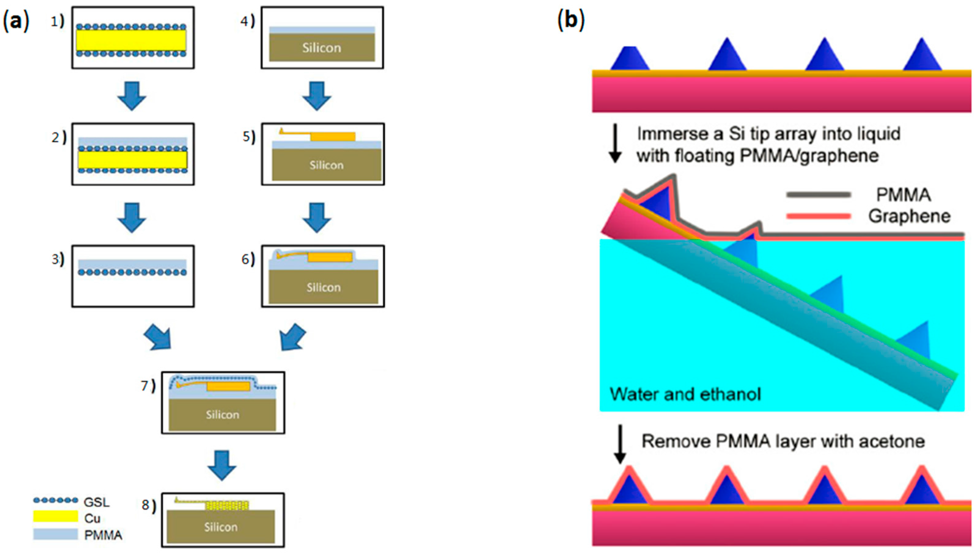
This kind of transfer method was also used in the work reported by Shim et al. [25], in which a 10–20 layer thick graphene stack grown on a 4-inch Ni/Si wafer (Graphene Laboratories Inc., Calverton, NY, USA) was used as graphene coating for scanning probe arrays. As usual, a ~70 nm thick PMMA layer was spin-coated on as-grown graphene/Ni/Si at 500 rpm for 10 s with a speed of 100 rpm, followed by 5000 rpm for 60 s with a speed of 1000 rpm. The PMMA/graphene/Ni/Si stack was preserved at room temperature for 24 h and dried naturally. Afterwards, small pieces (1 × 1 cm2) of wafer were immersed into aqueous FeCl3 solution (1 M) for etching away the Ni film, which produced the separation of the PMMA/graphene film from the substrate. Similarly, the PMMA/graphene film was rinsed with deionized water and then fished with the target substrate. In this case the authors designed a target substrate consisting on a transparent glass with 100 nm SiO2 with more than 4489 pyramidal tips (without cantilever, see Figure 2b) arranged in a matrix distribution. This target substrate was used to fish the PMMA/graphene stack, a process that was done by keeping a constant angle of 40° with respect to the liquid surface. The sample was exposed 48 h to air atmosphere at room temperature for natural drying, and the PMMA/graphene coated HSL tip array was immersed in acetone for 2 h to remove the PMMA. Finally, the sample was cleaned again in ethanol.
2.3. Mold-Assisted Transfer of CVD-Grown Graphene onto AFM Probes
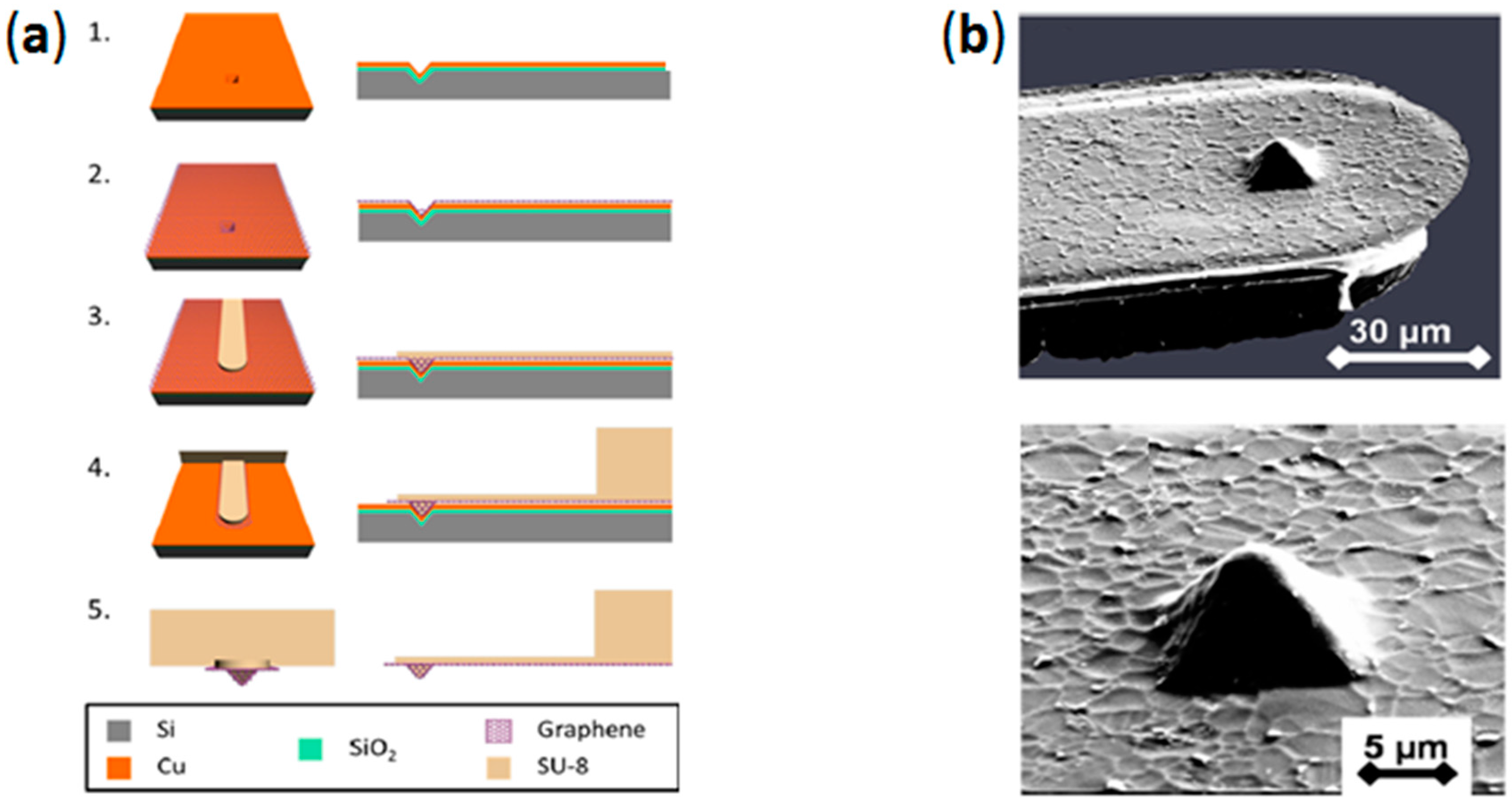
Martin-Olmos et al. [26] developed a different transfer method based on the use of a Cu mold, on which the graphene was grown before being filled with SU-8 photoresist. The entire fabrication process is displayed in Figure 3a.
First, a 100 nm SiO2/Si wafer was patterned with circles of different sizes (a few micrometers) via lithography. The sample was then immersed in potassium hydroxide (KOH) etchant to generate the inverted pyramids with different sizes, which were used as the molds for AFM tips. Thermal thin silicon dioxide (which served as a sacrificial layer) was grown on the patterned wafers, followed by the deposition of a 500 nm thick high-purity copper film, which acted as a catalytic metal for the CVD growth of graphene. In this case, the authors used a suitable metallic thickness that might be able to withstand the thermal heating during the 2D material growth. The molded substrates were heated in a tube furnace up to 800 ℃ under hydrogen gas flow of 5 sccm. Then, 35 sccm of methane (CH4) was introduced into the chamber, which produced the decomposition of methane and formation of monolayer graphene. The resulting graphene coated Cu mold was filled with SU-8 photoresist (10 μm) by using a spinner. Finally, the SU-8 photoresist was patterned by lithography and the substrate was etched: first the etching of SiO2 using KOH and then the Cu using FeCl3 (more experimental details can be found in Ref. [26]). The SEM images of the released SU-8 graphene coated nanoprobes (Figure 3b) show interesting and correct graphene coating on the SU-8 photoresist, which can be easily distinguished by the characteristic wrinkles.
2.4. Direct Graphite-Like Thin Film Deposition on AFM Nanoprobes
Graphene can be also successfully deposited on the apex of standard nanoprobes without the use of any CVD steps. Pacios et al. [27] reported the fabrication of an ultrathin graphite-coated AFM tip using a sputtering deposition followed by in situ annealing. First, a 30 nm thick amorphous carbon film was deposited on the as-received spherical Si/SiO2 or rounded Si bulk AFM tips via radio frequency (RF) sputtering. Then, a 100 nm thick platinum (Pt) catalyst film was directly deposited on the carbon film, also via RF sputtering. The process is highlighted in Figure 4a. The tip is then annealed in a quartz tube furnace under an argon atmosphere for 30 min at a temperature of 800 °C. This step produced the spreading of carbon from the graphite film into metal catalyst due to the high solubility of carbon in the Pt. When cooling down, the carbon separates and graphitic flakes are generated on the surface of the Pt film (see Figure 4b). Cross-section TEM images exhibited the successful growth of layered graphite film on the Pt-coated tips (Figure 4c,d). The thickness of the ultrathin graphite film obtained by this method is around 20 nm (see Figure 4d). For this experiment, the authors used AFM tips with different tip radiuses (ranging from 2 μm to 90 nm), heights (typically 10–15 μm) and force constants (ranging from 48 N/m to 0.2 N/m).
The advantages of this work are: (i) unlike thermal evaporation, in which carbon and Pt layers are evaporated in two separated chambers, here sputtering can produce both layers in the same run and the quality of the materials can be precisely controlled by the bias and pressure during the deposition process; (ii) the changeable directionality of sputtering helps to achieve full coverage for the irregular shapes of AFM tips; (iii) as a metal catalyst, platinum can provide better surface morphology and homogeneity for the growth of high quality 2D materials due to its higher melting temperature and lower thermal expansion coefficient; and (iv) Pt cannot be easily oxidized, in contrast with what happens to other metals (such as Ni or Cu), and its chemically inert property contributes to decreasing surface irregularities and keeping its catalytic ability. Compared to traditional CVD technology, the authors claim that this method is a clean, simple, less hazardous and reproducible technique, which makes it possible for large-scale manufacturing. In Figure 4c,d a cross-section of the graphitic film grown on the surface of the tip apex can be seen. Layered structure can be successfully obtained, as observed from the high resolution TEM images.
2.5. Liquid Phase Graphene Flakes Coated AFM Probes
Although AFM probes coated with graphene can be achieved by using some of the above- mentioned methodologies, complicated procedures are not advisable for the mass production needed in industry. Recently, high quality solution-processed graphene was used to coat different kinds of nanoprobes [28]. The graphene sheets were synthesized from graphite powder. Based on a series of redox reactions, graphite powder (2 g) was firstly oxidized by the Hummers–Offeman method with the assistance of H2SO4 (12 mL), K2S2O8 (3.0 g) and P2O5 (3.0 g) at 80 °C for 5 h. Then, H2SO4 (150 mL), KMnO4 (25 g) and 30 mL H2O2 were added to the resulting product in order to help to re-oxidize it, and thin flakes of graphene oxide were successfully obtained after: (i) washing (in 1:10 HCl and pure water), (ii) drying naturally, (iii) purifying (by dialysis for 1 week), and (iv) an ultrasonic bath. The 50 mL graphene oxide solution (0.1 mg/mL) was reduced by mixing it with hydration hydrazine (5 mL). The mix was then stirred for 24 h at 80 °C, filtered and dried, which resulted in a black powder graphene. Finally, the graphene solution was prepared by mixing the black graphene powder (5 mg) and pure water (1 mL), and sonicating at 50 W for 10 min. The resulting solution contained large amounts of graphene sheets with an average thickness of 0.7 nm and size of <1 μm. Currently there are several suppliers that provide these types of graphene solutions at a very low price. However, when selecting a graphene solution supplier one needs to verify that the solution really contains large area atomically thin graphene sheets, not just thick graphite particles. One recent study analyzed the size and thickness of the sheets in liquid phase exfoliated graphene from more than 20 different companies, and it was concluded that only two were able to provide micrometer scale sheets with thicknesses below 10 layers [36]. Also, several companies add polymers to the solution in order to stabilize it. It is important to select graphene solutions that do not use these polymers, as they may fall between the tip apex and the graphene flake, and result in a thick and non-conductive coating.
Once the solution is ready, coating the graphene tip is very simple, cheap and fast. In Hui‘s work [28], commercial AFM nanoprobes with a conductive coating of 20 nm Pt or PtIr from different manufacturers (Olympus and Bruker) were immersed in the graphene solution for less than one minute (see Figure 5). By swinging the probe, the graphene sheets readily attached to the sharp AFM tip by van der Waals forces. Van der Waals forces are much higher at very sharp morphologies [37], which means that all the flakes tend to attach there (i.e., many other locations of the nanoprobes remain uncoated, but very good conformal coating and high reproducibility is achieved at the tip apex). After that, the graphene coated nanoprobe was left to dry naturally. Alternatively, the nanoprobes coated by this method can also be dried using a N2 gun at a very low gas flow. N2 blowing also enhances the adhesion between the graphene and the tip apex. Additionally, the amount of graphene sheets attached to the tip apex can be tuned by adjusting the concentration of the graphene solution. This cost-efficient methodology could be used to achieve high-yields of graphene coated nanoprobes and facilitate their industrial production.
3. Perspectives on the Fabrication of Graphene Coated AFM Probes
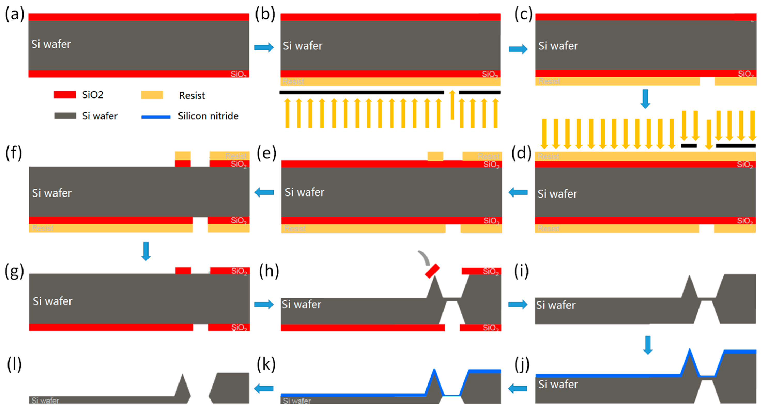
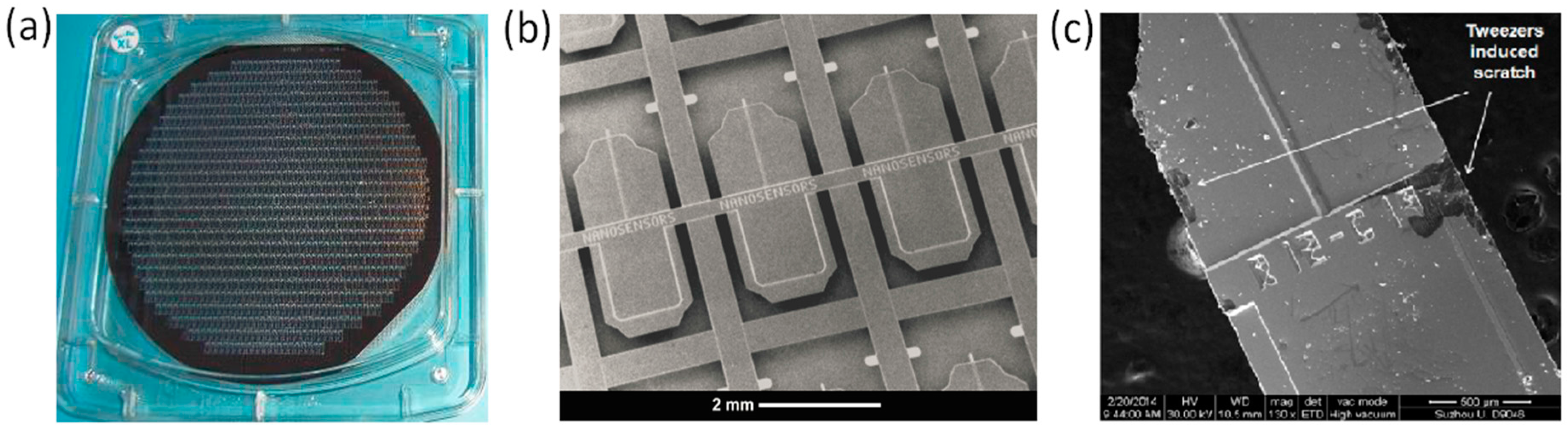
Based on the above discussions, liquid-phase exfoliated graphene coating seems to be the most promising methodology due to its low cost, fast coating process and excellent compatibility with industry. Here, the possible manufacturing procedure based on the current technologies being used by AFM tips manufacturers (such as Nanoworld) is proposed as follows [38]. The basic fabrication process of standard tips is described in Figure 6. A piece of silicon wafer is oxidized on both sides (Figure 6a). Then, a layer of photo resist is spin-coated onto the back side of the SiO2/Si/SiO2 wafer, and subsequently exposed to UV light using a mask (Figure 6b–c). Similarly, the front side is patterned by the same method but using a different mask (see Figure 6d–e). The silicon dioxide on the front side is removed by isotropic wet etching methodology (Figure 6f) and then the photoresist on both sides is dissolved (Figure 6g). The formation of probes can be observed after the anisotropic wet etching of silicon by KOH in the following steps, until the oxide shields falls off (as shown in image Figure 6h,i). A silicon nitride layer is deposited to protect the tip side of the probe from the damage through further wet etching of silicon, which defines the thickness of cantilever (Figure 6j,k). Finally, silicon bulk probes are isolated by removing the silicon nitride layer. In order to obtain functional coating probes, metallic or magnetic materials are required to be deposited on top of Si bulk probes by specific methods, such as sputtering, atomic layer deposition (ALD) and/or E-beam evaporation. This process is normally conducted on six-inch wafers (see Figure 7a), and after the process the chips are patterned within the silicon wafer (Figure 7b). Then, they need to be removed and placed in sticky boxes (using vacuum tweezers to avoiding scratches) for commercialization. The photograph of a wafer patterned with AFM tips, as well as the zoomed-in SEM images of the chips containing the cantilevers and sharp tips are shown in Figure 7a,b, respectively.
The coating process via liquid phase exfoliation presented in Ref. [28] has been carried out by manipulating probe tips one-by-one from commercial sticky boxes using standard tweezers, and immersing them into a tube containing the graphene solution. Despite the success and reproducibility of the experiments, this method should be optimized for the coating of several tips in parallel and avoid tip-induced scratch in the chip that contains the cantilever and tips (see Figure 7c). The ideal is that AFM tip manufacturers incorporate the graphene coating process at the end of the production chain of the AFM tips. To do so, the as-fabricated wafers containing the tips should be immersed in a container filled with graphene solution for a certain period of time. The concentration of the graphene solution, the immersion time and the use of agitation and/or voltage may be tuned to improve the percentage of tips coated and the quality of the coating.
4. Functionalities of Graphene Coated AFM Probes
Graphene coated AFM probes have been fabricated successfully by some of the methodologies described above. After fabrication, these devices show enhanced performance in several types of experiments such as, topographic and current maps, current-voltage curves, force-distance curves, as well as statistical analysis of variability and durability. Graphene coated nanoprobes have been used in different fields of science, including electronics, mechanics, and physics [23,24,25,26,27,28,29].
4.1. High Wear Resistance in Lateral Scans
The graphene coated SU-8 nanoprobes fabricated by mold-assisted graphene transfer [26] exhibited mechanical properties and conductivity different to those of uncoated (graphene-free) SU-8 probes. In experiments both tapping mode and contact mode images are collected on a calibration sample, which consists of 800 nm diameter and 40 nm thick Ag pillars on a SiO2 substrate, to characterize the polymer AFM probes. As shown in Figure 8a, under tapping mode, both probes can resolve the topographic information, and the scanned image using a graphene coated SU-8 probe shows similar resolution (10% loss) as the uncoated probe. This may a result of the slightly increased radius of the tip apex caused by the graphene layer (this indicates that the layer is not as thin as believed) and/or non-uniform surface of the graphene film. The interesting point came when scanning the sample in contact mode. The images scanned using uncoated (graphene-free) SU-8 probes show much lower lateral and vertical resolution than those collected using graphene coated ones, and the images appear blurry and with the profiles repeated. The characteristic doubled (repeated) features in the topographic scans are a clear indication that a tip with two apexes has been formed. This is related to the removal of some material at the tip apex; the volume loss in the tip can produce irregular shapes, making it possible that more than one location of the tip touches the sample, which results in repeated profiles along the scanned area.
The reason why the tip loses resolution so fast is the low hardness of the SU-8 material (~0.43 GPa [39], compared to Si ~11.9 GPa [40]), leading to the fast wearing of (volume removal) the apex after scanning the sample consecutively. This phenomenon has been confirmed by collecting current maps of 4 nm HfO2/1 nm SiO2 stacks (under a constant bias), using a new (top) and worn out (bottom) commercial conductive AFM (see Figure 8b). When the tip is new (top map) small conductive spots can be detected, indicating the flow of tunneling current across the ultra-thin bilayer insulator. On the contrary, the worn tip shows abundant ring-like conducting features (instead of spots, see bottom current map) which is related to the removal of the tip apex (see schematics in Figure 8b). Fortunately, the superb mechanical properties of graphene can effectively protect the apex from wearing even after several scans (see Figure 8c).
4.2. Avoiding Water Perturbations at the Tip–Sample Junction
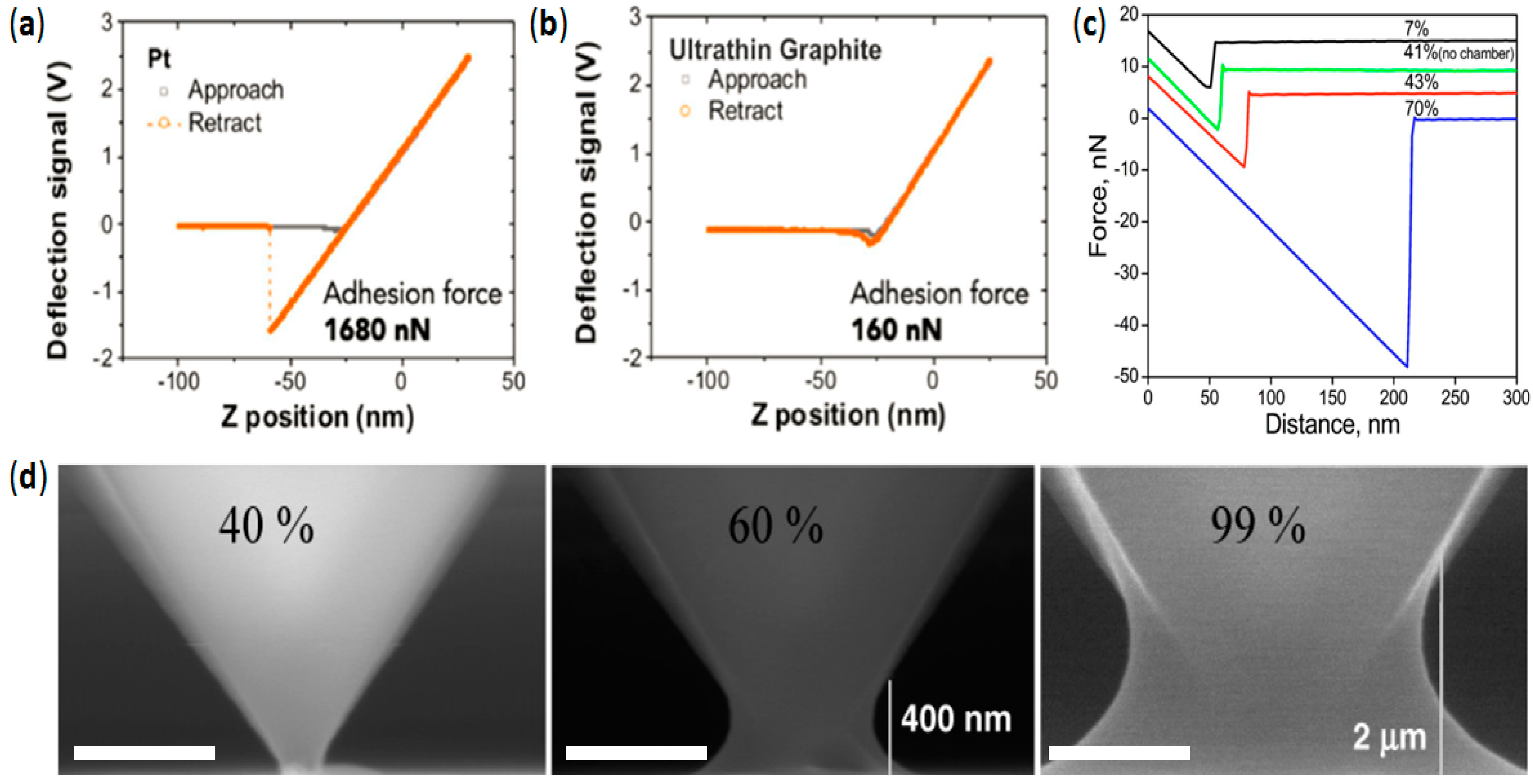
The interaction between the tips and a silicon substrate has been compared before and after graphene coating. Force-distance (F–Z) curves have been collected at several locations of the sample. The F–Z curves represent the vertical force that the tip applies to the surface of the sample, which varies with the distance between them. The force vertically applied is proportional to the deflection of the cantilever, and for this reason deflection-force (D–Z) curves can also give relevant information (the Y-axis in Figure 9a is deflection, not force, but this is also acceptable if relative variations want to be studied). The D–Z collected with the graphene-free Pt-varnished Si tip on the surface of a Si substrate shows the typical shape: (i) the force stays at zero when the tip is far away from the sample surface of the sample (Z << 0); (ii) starts to increase when the tip is in contact with the sample. In theory that should happen for Z > 0, but in Figure 9a the deflection starts to increase at Z ~ −25 nm; the reason is that the initial position of the tip is not at Z > 0, but a bit (~25 nm) above the surface of the sample in order to avoid damage of the tip); (iii) during tip retraction, a high negative peak can be observed, which is related to the adhesion (anti-repulsive) force between the tip and the sample and (iv) once the tip is beyond the limited distance this type of force suddenly disappears (a jump in the D-Z curve can be distinguished).
As shown in Figure 9a, the adhesion force detected in the D–Z curve performed with the Pt-coated AFM tip is 1680 nN. Interestingly, when the same experiment is carried out using a graphene coated tip (obtained with the graphite thin film deposition method explained in Section 2.4) the shape of the D–Z curve is similar, but the adhesion force is much smaller. While different materials at the tip apex may produce different tip-sample interactions, a feasible explanation for such a huge difference in the adhesion peak is as follows. The force that plays the major role in tip–sample adhesion in AFM experiments is due to capillary effects [41]. Basically, when an AFM tip is placed in contact with the sample in normal atmospheric conditions, a water layer related to the relative humidity is formed between the tip and a sample’s surface, which produces a water meniscus at the junction. The depth of the water layers and the size of the water meniscus increases with the relative humidity (see Figure 9d) [42]. Stukalov et al. [43] demonstrated that the contact force between a Si AFM tip and a mica substrate can increase greatly depending on the relative humidity (see Figure 9c). Taking into account that the reduction observed in Figure 9a,b is one order of magnitude, this indicates that graphene is an excellent material for avoiding tip-sample capillary effects, which are very annoying in several types of SPM experiments [44,45,46]. This observation can also be related to the hydrophobic nature of the graphene coating [47]. On the contrary, the Pt coating of the graphene-free tip is highly hydrophilic.
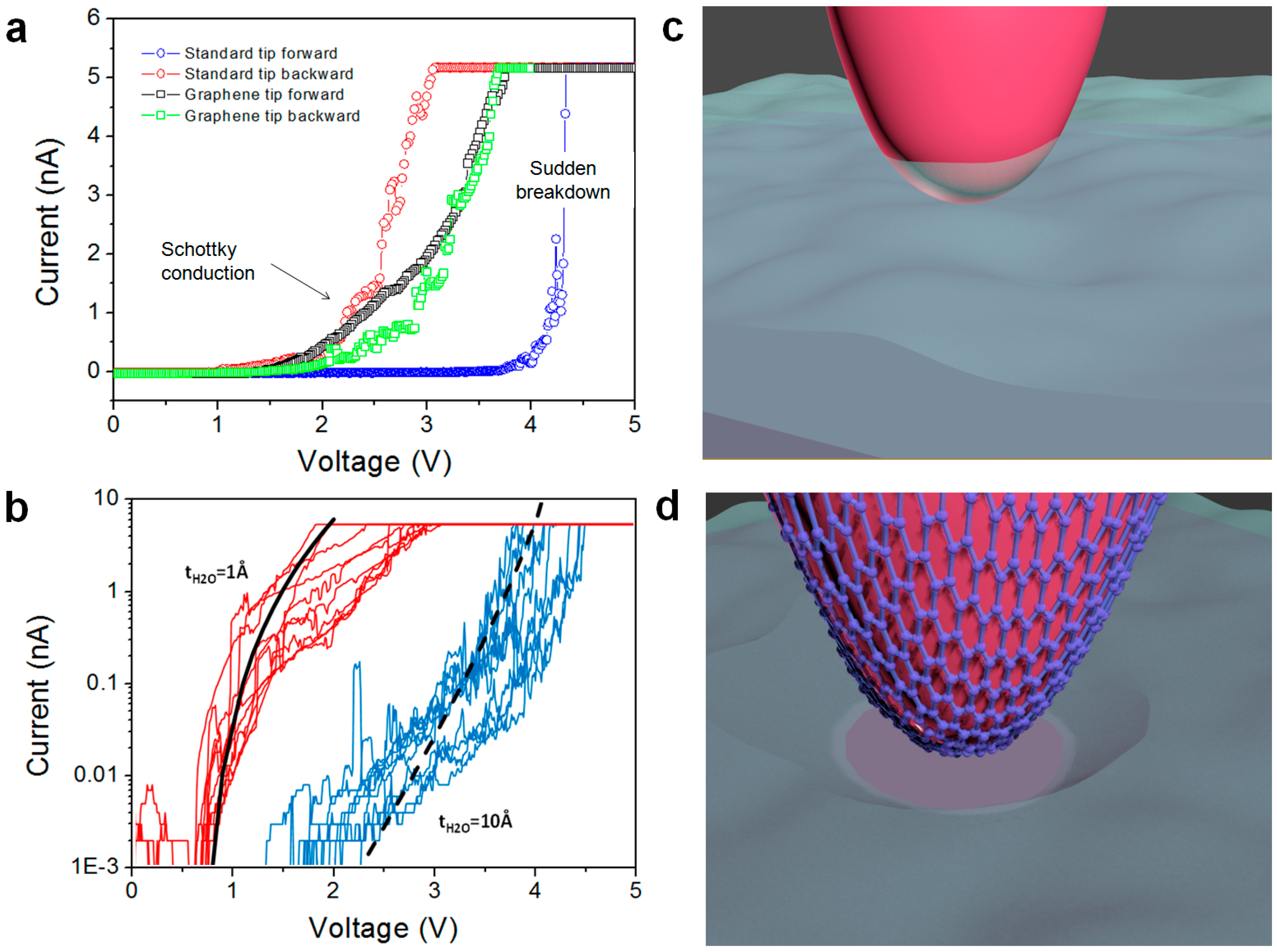
The effect of water meniscus minimization/removal at the tip-sample junction due to the graphene coating have very positive impact in several different types of experiments, especially in electronic measurements. Hui et al. [28] collected forward and backward current-voltage (I–V) curves on the surface of an n-type Si wafer using both standard PtIr varnished AFM tips with and without graphene coating (solution processed liquid-phase exfoliation graphene). The results are displayed in Figure 10a.
The standard tip shows a large onset potential (VON, defined as the minimum voltage that shows currents above the noise level) followed by a sharp current increase in the forward curve. Then, the backward tip shows a clear shift towards lower potentials, indicating that the tip-sample junction has become more conductive; moreover, the shape of this I–V curve is less sharp, and more similar to the typical conduction of silicon. On the contrary, the I–V curves collected with graphene coated AFM tips show currents similar to the backward curve collected with graphene-free tips. It should be highlighted that the expected conduction mechanism between the PtIr coating (in fact it is 95% Pt) and the n-type Si substrate (which has no native oxide, as it was removed via hydrofluoric acid) is Schottky conduction, and the observations during the forward I–V curve collected with the graphene-free PtIr-varnished tip are unexpected.
Nevertheless, this behavior can be explained by the presence of a water meniscus and a nanometric water layer between the graphene-free PtIr-varnished AFM tip and the sample. The water layer between the tip and the sample increases the resistivity at the junction, which is why VON is larger. When the electrical field is large enough current starts to flow and the tip physically contacts the n-type Si sample, which produces a shift in the I–V curve towards lower potentials. After that, the shape observed in the I–V curve is typical for Schottky conduction. To demonstrate this hypothesis, several I–V curves have been collected at different locations of the sample using the standard (graphene-free) tips, and the forward and backward I–V curves have been fitted to the conduction across a Pt/H2O/Si heterojunction (similar to the tip-sample junction) tuning the different H2O thicknesses. The fittings were done with the software MDLab [48]. As displayed in Figure 10b, the calculations indicate that the forward I–V curves (blue) can only be fitted using a H2O thickness of 10 Å, while the backward I–V curves can be fitted with an almost negligible H2O thickness of 1 Å, respectively. In contrast, graphene coated AFM tips do not show this problem (see Figure 10c,d), and the currents registered are real (correct) from the initial (forward) I–V curve. Again, the hydrophobic nature of the graphene coating had a positive influence on the measurements.
Lanza et al. [29] has proved this by studying the electrical behaviors of HfO2/Si stacks using as-received AFM tips (Figure 11a–c) and graphene coated AFM tips (Figure 11d–f), respectively. As shown in Figure 11, topographic and current maps were collected simultaneously under a contact force of 0.1 nN and voltage of 2 V in a high vacuum environment (10−7 torr). Comparing these two current maps (white represents 0 pA), it is obvious that the dark spots, which represent the local currents through HfO2, are smaller in Figure 11e than the current collected by the uncoated AFM tip (Figure 11b). Also, the statistical analysis shown in Figure 11c,f corroborate the smaller size of the conductive spots collected using graphene coated tips and an obvious shift to higher currents compared to uncoated ones (insets in Figure 11c,f), which further shows a lower tip-sample contact area for the graphene-coated tips due to keeping good conductivity. In general, the smoother topographic surface and individual conductive spots observed in Figure 11 demonstrate that the graphene-coated AFM tips possess not only high lateral resolution, but also superior electrical performance.
4.3. Lower Data Variability
Before analyzing the variability of graphene coated nanoprobes, the intrinsic variability of standard (graphene-free) probes should be discussed. The variability of standard nanoprobes is mainly affected by two factors: (i) the variability of the parameters of the tips (tip radius and spring constant). It is important to note that the manufacturers of AFM probes allow deviations of the tip radius up to 100% (e.g., from 100 nm to 200 nm [49]), and the typical ranges for spring constant deviations can be as high as one order of magnitude (e.g., from 1.5 N/m to 18.3 N/m [49]); and (ii) the presence of a water meniscus at the tip-sample junction. Standard AFM probes varnished with metal are hydrophilic (which can form a thick water meniscus at the junction, see Figure 9d), while graphene-coated probes are hydrophobic (which repulses the water from the tip and produces a clean junction). Different amounts of water at the junction can have a huge effect in experiments, especially when measuring adhesion force (see Figure 9) or currents (see Figure 10 and Refs. [50,51]). In this section, the effect of the graphene coating on these two sources of variability is analyzed.
When discussing the variability of the tip radius and spring constant induced by the graphene coating, the observations are clear: the effect of the graphene coating on these two parameters is much lower than the intrinsic variability provided by the manufacturer. First, the typical thickness of the graphene sheets used to coat the tips in the liquid-phase exfoliated method (which is the most promising) varies from one to five layers, which equals 0.46 nm–2.3 nm. Second, the mass of the graphene nanosheets used in the liquid-phase exfoliated method is negligible, which does not modify the spring constant of the cantilever [28]. The effect of the graphene coating may be much more relevant if its thickness and area is increased (for example, using the graphite-like film deposition method described in Section 2.4).
Regarding the variability induced by the water meniscus, the use of graphene coating is beneficial because it reduces (if not completely removes) the presence of water at the junction. Therefore, this should result in even lower variability compared to its graphene-free counterparts. Wen et al. [23] statistically collected several groups of I–V curves in octanemonothiol-based molecular junctions using both graphene-free and graphene coated Au-varnished nanoprobes (fabricated via direct CVD-growth on the surface of the Au varnish), leading to two types of molecular junctions, Au/octanemonothiol/Au (Figure 12a) and Au/octanemonothiol/graphene/Au (Figure 12b). In total, more than 1000 curves are collected using 18 tips, and each line in the plots represents the average of 100 I–V curves. Comparing them, larger tip-to-tip variance in current up to 3 orders of magnitude has been detected in the molecular junctions without graphene. Additionally, a relatively small variation of less than 1 order of magnitude has been detected using graphene coated nanoprobes as molecular junction.
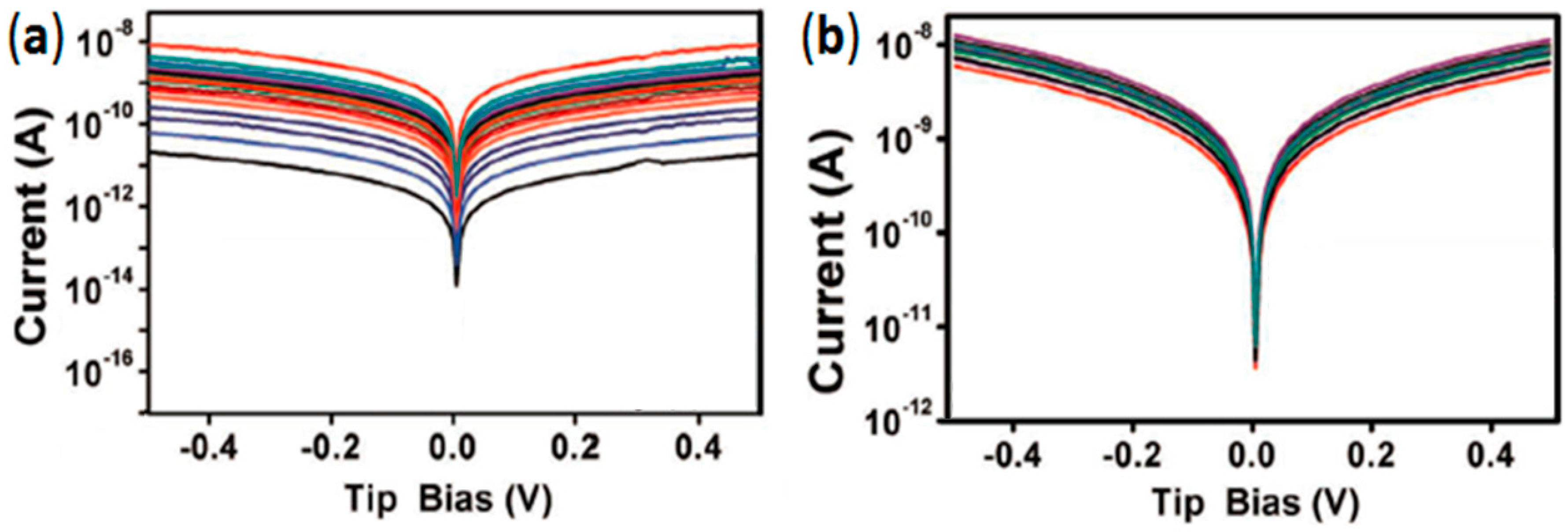
Statistical analyses of the experimental data using nanoprobes coated with graphene via liquid-phase exfoliation method have been also carried out [28,52]. More than 100 I–V curves collected on a native oxide free n-type Si substrate have been collected (see Figure 13a,b) for each type of tip. In order to avoid big differences related to the presence of water between the tip and the sample, only backward curves have been considered (see also explanations related to Figure 10). Despite using only backward curves the results still show that both the onset potential and the variability is smaller when using graphene coated nanoprobes. Finally, groups of I–V curves have been measured with the same types of tips on a metallic substrate. The plots show saturation of the currents at ±5 nA, with a linear shape going from −5 nA to +5 nA. The saturation voltage (voltage at which the I–V curves reach 5 nA) has been evaluated statistically. Figure 13c shows that the variability of the data is not only smaller when using graphene coated AFM tips, but also the variability when comparing different devices is much smaller. Hui et al. [28] advise that the smaller onset voltage of the graphene coated probes may be affected by the different work functions between Pt and graphene tip electrodes. Indeed, the work function of the probes varies from ~6.1 eV (Pt) to ~4.8 eV (Pt/graphene) [53], as well as the absence of water perturbations, together contributing to the smaller onset voltage and the variability of I–V curves.
4.4. High Stability vs. High Currents and Mechanical Strains: Enhanced Lifetime
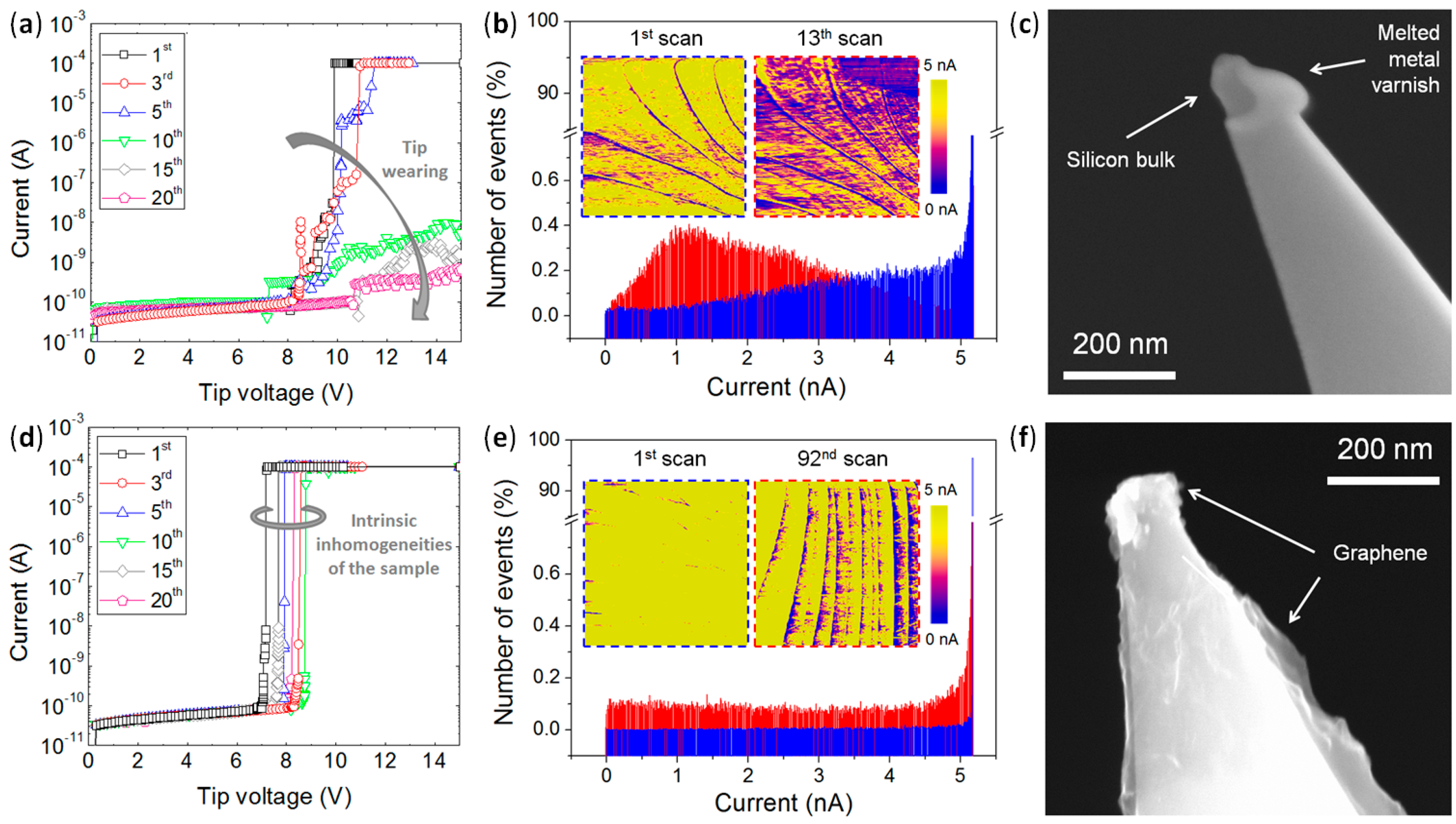
This is probably one of the properties that can bring most benefit to the users of graphene coated nanoprobes. Graphene coated nanoprobes fabricated by various methods have been demonstrated to have superior stability when performing different types of experiments (see Figure 14). Lanza et al. [24] performed an experiment that consisted of collecting several I-V curves at different (randomly selected) locations of a 3 nm thick HfO2 stack (in order to monitor the tunneling currents and dielectric breakdown) using standard and graphene coated AFM tips (fabricated via CVD graphene transfer). The main characteristic was that a source meter was connected directly to the tip of the CAFM, so that high voltages (>10 V) and high currents (up to mA) could be registered [54]. While the graphene coated AFM tip is able to distinguish the dielectric breakdown at several different locations (Figure 14d), the standard tip cannot withstand the high currents (the current is 10−4 A, therefore, the current density is 108 A/cm2 because the typical effective area at the tip-sample junction for this sample is 100 nm2), and shows obvious current reduction with total conductivity degradation after 5 I–V curves.
In a different experiment by Hui et al. [28], the durability of the graphene-free and graphene coated tips (using a liquid-phase exfoliation method) was analyzed via current maps collected on highly conductive samples (graphene/Cu foils) under a constant bias of 1 V and a deflection setpoint of 4 V. As shown in Figure 14b,e, while the standard CAFM tip lost its conductivity in just 13 scans (Figure 14b), the graphene-coated tip kept good conductivity even after 92 scans (Figure 14e). In the first experiment (Figure 14a,d) the tip was held static at one position on the sample; therefore, the lateral friction was minimal and the wearing was related to the high currents. On the contrary (Figure 14b,e), the most harmful thing for the tips was the friction, as the currents did not increase above the nanometer scale. In any case, graphene coated AFM tips showed good stability vs. these harmful tests. In Figure 14c, an AFM tip degraded in a static experiment driving large currents can be observed via SEM; the metallic varnishes that provide high conductivity melted. In Figure 14f an SEM image of a graphene coated tip after a sequence of current maps can be observed. No degradation is detected, other than small particles attached to the tip during the scans.
Apart from all the above benefits, more recently graphene coated colloidal probes, i.e., SiO2 microspheres, were developed to achieve an ultra-low and robust friction coefficient of 0.003 under high contact pressure, in which the super-lubricity of graphite and graphene plays a significant role [55]. Moreover, other properties of graphene, such as, flexibility, transparency, and low toxicity, enable the graphene coated probes to be competitive in the development of flexible and transparency microelectromechanical systems, as well as medical diagnosis.
5. Conclusions
In conclusion, different approaches using CVD growth, CVD transfer, sputtering and liquid phase exfoliated graphene have been used to coat nanoprobes with graphene. Direct CVD growth is highly questionable because the high temperatures used can damage the tip, and CVD transfer is too expensive due to the involvement of human labor. Direct sputtering shows good performance but the thermal budget is also high. So far, the liquid phase exfoliated approach has proved to be the cheapest and most industry-compatible method. All graphene coated nanoprobes show lifetimes much longer than their uncoated counterparts when used in different experiments. Specifically, they possess high wear resistance, stability and mechanical strength, as well as lower variability, which enables the application of the graphene-coated nanoprobes in the fields of electronics, mechanics and biology in the near future. In order to truly realize the manufacturing of graphene coated probes in industry, systematic techniques need to be further undertaken and optimized for mass production.
Acknowledgments
This work has been supported by the Young 1000 Global Talent Recruitment Program of the Ministry of Education of China, the National Natural Science Foundation of China (grants no. 61502326, 41550110223, 11661131002), the Jiangsu Government (grant no. BK20150343), the Ministry of Finance of China (grant no. SX21400213) and the Young 973 National Program of the Chinese Ministry of Science and Technology (grant no. 2015CB932700). The Collaborative Innovation Center of Suzhou Nano Science & Technology, the Jiangsu Key Laboratory for Carbon-Based Functional Materials & Devices, the Priority Academic Program Development of Jiangsu Higher Education Institutions, the 111 Project from the State Administration of Foreign Experts Affairs, and the Opening Project of Key Laboratory of Microelectronic Devices & Integrated Technology (Institute of Microelectronics, Chinese Academy of Sciences) are also acknowledged.
Conflicts of Interest
The authors declare no conflict of interest.
References
- Ji, Y.; Pan, C.; Zhang, M.; Long, S.; Lian, X.; Miao, F.; Hui, F.; Shi, Y.; Larcher, L.; Wu, E.; et al. Boron nitride as two dimensional dielectric: reliability and dielectric breakdown. Appl. Phys. Lett. 2016, 108, 012905. [Google Scholar] [CrossRef]
- Song, X.; Hui, F.; Gilmore, K.; Wang, B.; Jing, G.; Fan, Z.; Grustan-Gutierrez, E.; Shi, Y.; Lombardi, L.; Hodge, S.A.; et al. Enhanced piezoelectric effect at the edges of stepped molybdenum disulfide. Nanoscale 2017, 9, 6237–6245. [Google Scholar] [CrossRef] [PubMed]
- Paxton, W.F.; Spruell, J.M.; Stoddart, J.F. Heterogeneous catalysis of a copper-coated atomic force microscopy tip for direct-write click chemistry. J. Am. Chem. Soc. 2009, 131, 6692–6694. [Google Scholar] [CrossRef] [PubMed]
- Park, K.D.; Raschke, M.B.; Jang, M.J.; Kim, J.H.; O, B.H.; Park, S.G.; Lee, E.H.; Lee, S.G. Near-field imaging of cell membranes in liquid enabled by active scanning probe mechanical resonance control. J. Phys. Chem. C. 2016, 120, 21138–21144. [Google Scholar] [CrossRef]
- Pan, N.; Rao, W.; Standke, S.J.; Yang, Z. Using dicationic ion-pairing compounds to enhance the single cell mass spectrometry analysis using the single-probe: A microscale sampling and ionization device. Anal. Chem. 2016, 88, 6812–6819. [Google Scholar] [CrossRef] [PubMed]
- Bining, G.; Quate, C.F.; Gerber, C. Atomic Force Microscope. Phys. Rev. Lett. 1986, 56, 930–933. [Google Scholar] [CrossRef] [PubMed]
- Kawahara, K.; Shirasawa, T.; Lin, C.L.; Nagao, R.; Tsukahara, N.; Takahashi, T.; Arafune, R.; Kawai, M.; Takagi, N. Atomic structure of “multilayer silicene” grown on Ag(111): Dynamical low energy electron diffraction analysis. Surf. Sci. 2016, 651, 70–75. [Google Scholar] [CrossRef]
- Hafner, J.H.; Cheung, C.L.; Woolley, A.T.; Lieber, C.M. Structural and functional imaging with carbon nanotube AFM probes. Prog. Biophys. Mol. Biol. 2001, 77, 73–110. [Google Scholar] [CrossRef] [Green Version]
- Yapici, M.K.; Lee, H.; Zou, J.; Liang, H. Gold-coated scanning probes for direct “write” of sub-micron metallic structures. Micro Nano Lett. 2008, 3, 90–94. [Google Scholar] [CrossRef]
- Boggild, P.; Hansen, T.M.; Kuhn, O.; Grey, F. Scanning nanoscale multiprobes for conductivity measurements. Rev. Sci. Instrum. 2000, 7, 2781–2783. [Google Scholar] [CrossRef] [Green Version]
- Lanza, M. Conductive Atomic Force Microscopy: Applications in Nanomaterials; Wiley-VCH Berlin: Berlin, Germany, 2017; ISBN 978-3-527-34091-0. [Google Scholar]
- Hoefflinger, B. The International Technology Roadmap for Semiconductors (ITRS), 2001 ed.; Springer: Berlin, Germany, 2001. [Google Scholar]
- Nourbakhsh, A.; Zubair, A.; Sajjad, R.N.; Amir, T.K.G.; Chen, W.; Fang, S.; Ling, X.; Kong, J.; Dresselhaus, M.S.; Kaxiras, E.; et al. MoS2 field-effect transistor with sub-10 nm channel length. Nano Lett. 2016, 16, 7798–7806. [Google Scholar] [CrossRef] [PubMed]
- Xu, K.; Chen, D.; Yang, F.; Wang, Z.; Yin, L.; Wang, F.; Cheng, R.; Liu, K.; Xiong, J.; Liu, Q.; et al. Sub-10 nm nanopattern architecture for 2D material field-effect transistors. Nano Lett. 2017, 17, 1065–1070. [Google Scholar] [CrossRef] [PubMed]
- Dai, H.J.; Hafner, J.H.; Rinzler, A.G.; Colbert, D.T.; Smalley, R.E. Nanotubes as nanoprobes in scanning probe microscopy. Nature 1996, 384, 147–150. [Google Scholar] [CrossRef]
- Xu, J.; Shingaya, Y.; Zhao, Y.; Nakayama, T. In situ, controlled and reproducible attachment of carbon nanotubes onto conductive AFM tip. Appl. Surf. Sci. 2015, 335, 11–16. [Google Scholar] [CrossRef]
- Tay, A.B.H.; Thong, J.T.L. Fabrication of super-sharp nanowire atomic force microscope probes using a field emission induced growth technique. Rev. Sci. Instrum. 2004, 75, 3248–3255. [Google Scholar] [CrossRef]
- Bakhti, S.; Destouches, N.; Hubert, C.; Reynaud, S.; Vocanson, F.; Ondarcuhu, T.; Epicier, T. Growth of single gold nanofilaments at the apex of conductive atomic force microscope tips. Nanoscale 2016, 8, 7496–7500. [Google Scholar] [CrossRef] [PubMed]
- Neto, A.H.C.; Guinea, F.; Peres, N.M.R.; Novoselov, K.S.; Geim, A.K. The electronic properties of graphene. Rev. Mod. Phys. 2009, 81, 109. [Google Scholar] [CrossRef]
- Chen, S.; Brown, L.; Levendorf, M.; Cai, W.; Ju, S.Y.; Edgeworth, J.; Li, X.; Magnuson, C.W.; Velamakanni, A.; Piner, R.D.; et al. Oxidation resistance of graphene-coated Cu and Cu/Ni alloy. ACS Nano 2011, 5, 1321. [Google Scholar] [CrossRef] [PubMed]
- Lee, C.; Wei, X.; Kysar, J.W.; Hone, J. Measurement of the elastic properties and intrinsic strength of monolayer graphene. Science 2008, 321, 385. [Google Scholar] [CrossRef] [PubMed]
- Balandin, A.; Ghosh, S.; Bao, W.; Calizo, I.; Teweldebrhan, D.; Miao, F.; Lau, C.N. Superior thermal conductivity of single-layer graphene. Nano Lett. 2008, 8, 902. [Google Scholar] [CrossRef] [PubMed]
- Wen, Y.; Chen, J.Y.; Guo, Y.; Wu, B.; Yu, G.; Liu, Y. Multilayer graphene-coated atomic force microscopy tips for molecular junctions. Adv. Mater. 2012, 24, 3482–3485. [Google Scholar] [CrossRef] [PubMed]
- Lanza, M.; Bayerl, A.; Gao, T.; Porti, M.; Nafria, M.; Jing, G.Y.; Zhang, Y.F.; Liu, Z.F.; Duan, H.L. Graphene-coated atomic force microscope tips for reliable nanoscale electrical characterization. Adv. Mater. 2013, 25, 1440–1444. [Google Scholar] [CrossRef] [PubMed]
- Shim, W.; Brown, K.A.; Zhou, X.Z.; Rasin, B.; Liao, X.; Mirkin, C.A. Multifunctional cantilever-free scanning probe arrays coated with multilayer graphene. Proc. Natl. Acad. Sci. USA 2012, 109, 18311–18317. [Google Scholar] [CrossRef] [PubMed]
- Martin-Olmos, C.; Rasool, H.I.; Weiller, B.H.; Gimzewski, J.K. Graphene MEMS: AFM probe performance improvement. ACS Nano 2013, 7, 4164–4170. [Google Scholar] [CrossRef] [PubMed]
- Pacios, M.; Hosseini, P.; Fan, Y.; He, Z.; Krause, O.; Hutchison, J.; Warner, J.H.; Bhasskaran, H. Direct manufacturing of ultrathin graphite on three-dimensional nanoscale features. Sci. Rep. 2016, 6, 22700. [Google Scholar] [CrossRef] [PubMed]
- Hui, F.; Vajha, P.; Shi, Y.; Ji, Y.; Duan, H.; Padovani, A.; Larcher, L.; Li, X.R.; Xu, J.J.; Lanza, M. Moving graphene devices from lab to market: Advanced graphene-coated nanoprobes. Nanoscale 2016, 8, 8466–8473. [Google Scholar] [CrossRef] [PubMed]
- Lanza, M.; Gao, T.; Yin, Z.; Zhang, Y.; Liu, Z.; Tong, Y.; Shen, Z.; Duan, H. Nanogap based graphene coated AFM tips with high spatial resolution, conductivity and durability. Nanoscale 2015, 5, 10816–10823. [Google Scholar] [CrossRef] [PubMed]
- Kim, K.S.; Zhao, Y.; Jang, H.; Lee, S.Y.; Kime, J.M.; Kim, K.S.; Ahn, J.H.; Kim, P.; Choi, J.Y.; Hong, B.H. Large-scale pattern growth of graphene films for stretchable transparent electrodes. Nature 2009, 457, 706. [Google Scholar] [CrossRef] [PubMed]
- Xue, Y.Z.; Wu, B.; Guo, Y.L.; Huang, L.P.; Jiang, L.; Chen, J.Y.; Geng, D.C.; Liu, Y.Q.; Hu, W.P.; Yu, G. Synthesis of large-area, few-layer graphene on iron foil by chemical vapor deposition. Nano Res. 2011, 4, 1208. [Google Scholar] [CrossRef]
- Reina, A.; Thiele, S.; Jia, X.; Bhaviripudi, S.; Dresselhaus, M.S.; Schaefer, J.A.; Kong, J. Growth of large-area single- and bi-layer graphene by controlled carbon precipitation on polycrystalline Ni surfaces. Nano Res. 2009, 2, 509–516. [Google Scholar] [CrossRef] [Green Version]
- Nam, J.; Kim, D.C.; Yun, H.; Shin, D.H.; Nam, S.; Lee, W.K.; Hwang, J.Y.; Lee, S.W.; Weman, H.; Kim, K.S. Chemical vapor deposition of graphene on platinum: Growth and substrate interaction. Carbon 2017, 111, 733–740. [Google Scholar] [CrossRef]
- Li, X.; Cai, W.; Colombo, L.; Ruoff, R.S. Evolution of graphene growth on Ni and Cu by carbon isotope labeling. Nano Lett. 2009, 9, 4268–4272. [Google Scholar] [CrossRef] [PubMed]
- Uchida, Y.; Iwaizako, T.; Mizuno, S.; Tsuji, M.; Ago, H. Epitaxial chemical vapor deposition growth of monolayer hexagonal boron nitride on Cu(111)/sapphire substrate. Phys. Chem. Chem. Phys. 2017, 19, 8230–8235. [Google Scholar] [CrossRef] [PubMed]
- Castro-Neto, A.H. Plenary talk in Graphchina 2016, Qingdao (China). 22–24 September.
- Yang, L.; Hu, J.H.; Qin, J. The van der waals force between arbitrary-shaped particle and a plane surface connected by a liquid bridge in humidity environment. Granul. Matter 2014, 16, 903–909. [Google Scholar] [CrossRef]
- Russell, P. AFM Probe Manufacturing. AFM TIP Webinar. Available online: https://www.agilent.com/cs/library/slidepresentation/Public/AFM%20Probe%20ManufacturingNanoworld_tip_technologyPRussell07.pdf (accessed on 10 November 2008).
- Al-Halhouji, A.T.; Kampen, I.; Krah, T.; Büttgenbach, S. Nanoindentation Testing of SU-8 Photoresist Mechanical Properties. Microelectron. Eng. 2008, 85, 942–944. [Google Scholar] [CrossRef]
- Bhushan, B.; Li, X.D. Micromechanical and Tribological Characterization of Doped Single-Crystal Silicon and Polysilicon Films for Microelectromechanical Systems Devices. J. Mater. Res. 1997, 12, 54–63. [Google Scholar] [CrossRef]
- Cappella, B.; Dietler, G. Force-distance curves by atomic force microscopy. Surf. Sci. Rep. 1999, 34, 1–104. [Google Scholar] [CrossRef]
- Weeks, B.L.; Vaughn, M.W. Direct imaging of meniscus formation in atomic force microscopy using environmental scanning electron microscopy. Langmuir 2015, 21, 8096–8098. [Google Scholar] [CrossRef] [PubMed]
- Stukalov, O.; Murray, C.A.; Jacina, A.; Dutcher, J.R. Relative humidity control for atomic force microscopes. Rev. Sci. Instrum. 2006, 77, 033704. [Google Scholar] [CrossRef]
- Yang, G.; Vesenka, J.P.; Bustamante, C.J. Effects of tip-sample forces and humidity on the imaging of DNA with a scanning force microscope. Scanning 1996, 18, 344–350. [Google Scholar] [CrossRef]
- Ebenstein, Y.; Nahum, E.; Banin, U. Tapping mode atomic force microscopy for nanoparticle sizing: Tip-sample interaction effects. Nano Lett. 2002, 2, 945–950. [Google Scholar] [CrossRef]
- Xiao, X.; Qian, L. Investigation of humidity-dependent capillary force. Langmuir 2000, 16, 8153–8158. [Google Scholar] [CrossRef]
- Li, D.; Muller, M.B.; Gilje, S.; Kaner, R.B.; Wallace, G.G. Processable aqueous dispersions of graphene nanosheets. Nat. Nanotech. 2008, 3, 101–105. [Google Scholar] [CrossRef] [PubMed]
- Puglisi, F.M.; Larcher, L.; Pan, C.; Xiao, N.; Shi, Y.; Hui, F.; Lanza, M. 2D h-BN based RRAM devices. Proceedings of 2016 IEEE International Electron Devices Meeting (IEDM), San Francisco, CA, USA, 3–7 December 2016. [Google Scholar]
- Conductive Diamond Coated Tip-Force Modulation Mode-Reflex Coating. Available online: http://www.nanosensors.com/Conductive-Diamond-Coated-Tip-Force-Modulation-Mode-Reflex-Coating-afm-tip-CDT-FMR (accessed on 2 August 2017).
- Lanza, M.; Porti, M.; Nafría, M.; Aymerich, X.; Wittaker, E.; Hamilton, B. Electrical resolution during Conductive AFM measurements under different environmental conditions and contact forces. Rev. Sci. Instrum. 2010, 81, 106110. [Google Scholar] [CrossRef] [PubMed]
- Lanza, M.; Porti, M.; Nafría, M.; Aymerich, X.; Wittaker, E.; Hamilton, B. UHV CAFM characterization of high-k dielectrics: effect of the technique resolution on the pre- and post-breakdown electrical measurements. Microelectron. Reliab. 2010, 50, 1312–1315. [Google Scholar] [CrossRef]
- Hui, F.; Vajha, P.; Ji, Y.; Pan, C.; Grustan-Gutierrez, E.; Duan, H.; He, P.; Ding, G.; Shi, Y.; Lanza, M. Variability of graphene devices fabricated using graphene inks: atomic force microscope tips. Surf. Coat. Tech. 2017, 320, 391–395. [Google Scholar] [CrossRef]
- Khomyakov, P.A.; Giovannetti, G.; Rusu, P.C.; Brocks, G.; Brink, H.; Kelly, P.J. First-principles study of the interaction and charge transfer between graphene and metals. Phys. Rev. 2009, 79, 195425. [Google Scholar] [CrossRef]
- Blasco, X.; Nafria, M.; Aymerich, X. Enhanced electrical performance for conductive atomic force microscopy. Rev. Sci. Instrum. 2005, 76, 016105. [Google Scholar] [CrossRef]
- Liu, S.W.; Wang, H.P.; Xu, Q.; Ma, T.B.; Yu, G.; Zhang, C.; Geng, D.; Yu, Z.; Zhang, S.; Wang, W.; et al. Robust microscale superlubricity under high contact pressure enabled by graphene-coated microsphere. Nat. Commun. 2017, 8, 14029. [Google Scholar] [CrossRef] [PubMed]
Figure 1.
Direct chemical vapor deposition of graphene on metal-varnished AFM tips. (a) Schematic representation of an Au-varnished AFM tip coated with graphene that is being used as top electrode in a molecular junction; (b) Raman spectrum of the graphene formed on the Au electrode (red) and Au-coated AFM tip (black line); (c) SEM image of the tip apex after the CVD process. The surface appears to be covered by a discontinuous and thick layer, rather than atomically-thin continuous graphene. Reproduced with permission from [23], copyright Wiley-VCH (2012).

Figure 2.
Transfer of CVD-grown graphene onto AFM probe tips. (a) Step-by-step schematic of the process followed to transfer graphene (grown on Cu foils) onto AFM tips. Reproduced with permission from [24], copyright Wiley-VCH (2013): (b) Experimental protocol used to fabricate graphene coated tip arrays. Reproduced with permission from [25], copyright AAAS.

Figure 3.
Schematic of graphene coated SU-8 AFM probes obtained by CVD graphene transfer using a mold. (a) Fabrication procedure of graphene coated SU-8 AFM probes; (b) SEM images of released graphene coated SU-8 AFM probes (top) and zoom in probe apex (bottom). Reproduced with permission from [26], copyright ACS Nano (2013).

Figure 4.
Ultrathin graphite growth on high aspect ratio features. (a) Schematic of the growth process on a 3D shaped AFM nanoprobe; (b) Growth mechanism of thin graphite by thin film deposition technology and thermal annealing; Cross-sectional TEM image of the resulting graphite coated AFM tip in low (c) and high (d) magnification. Reproduced with permission from [27], copyright Springer Nature Publishing Group (2016).
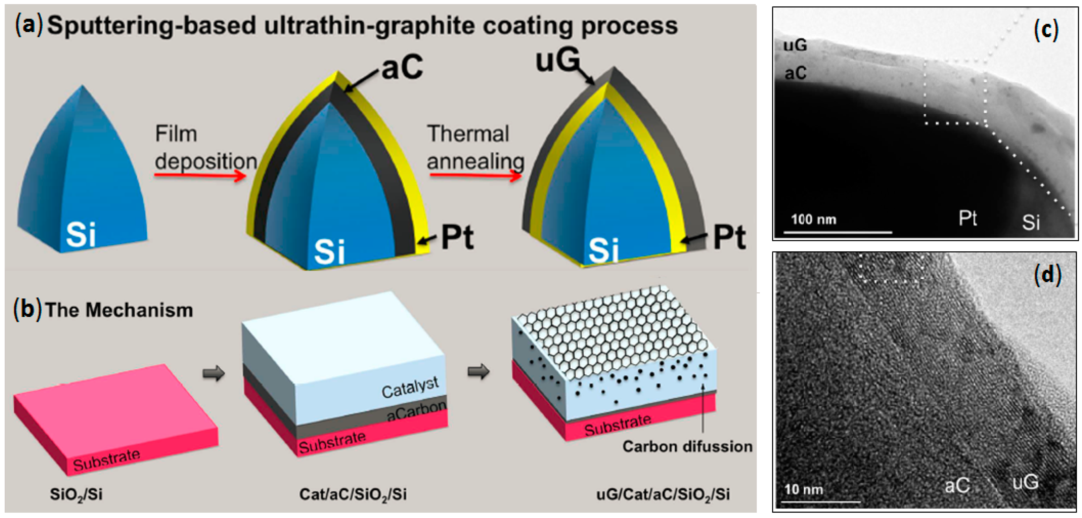
Figure 5.
Different commercial Pt-varnished AFM probes coated by solution processed graphene flakes. SEM images of as-received OMCL-AC240 nanoprobe before (a) and after coating (b); (c,d) are OSCM-PT and SCM-PIC AFM nanoprobes coated with low density of graphene sheets (respectively). Reproduced with permission from [28], copyright The Royal Society of Chemistry (2016).
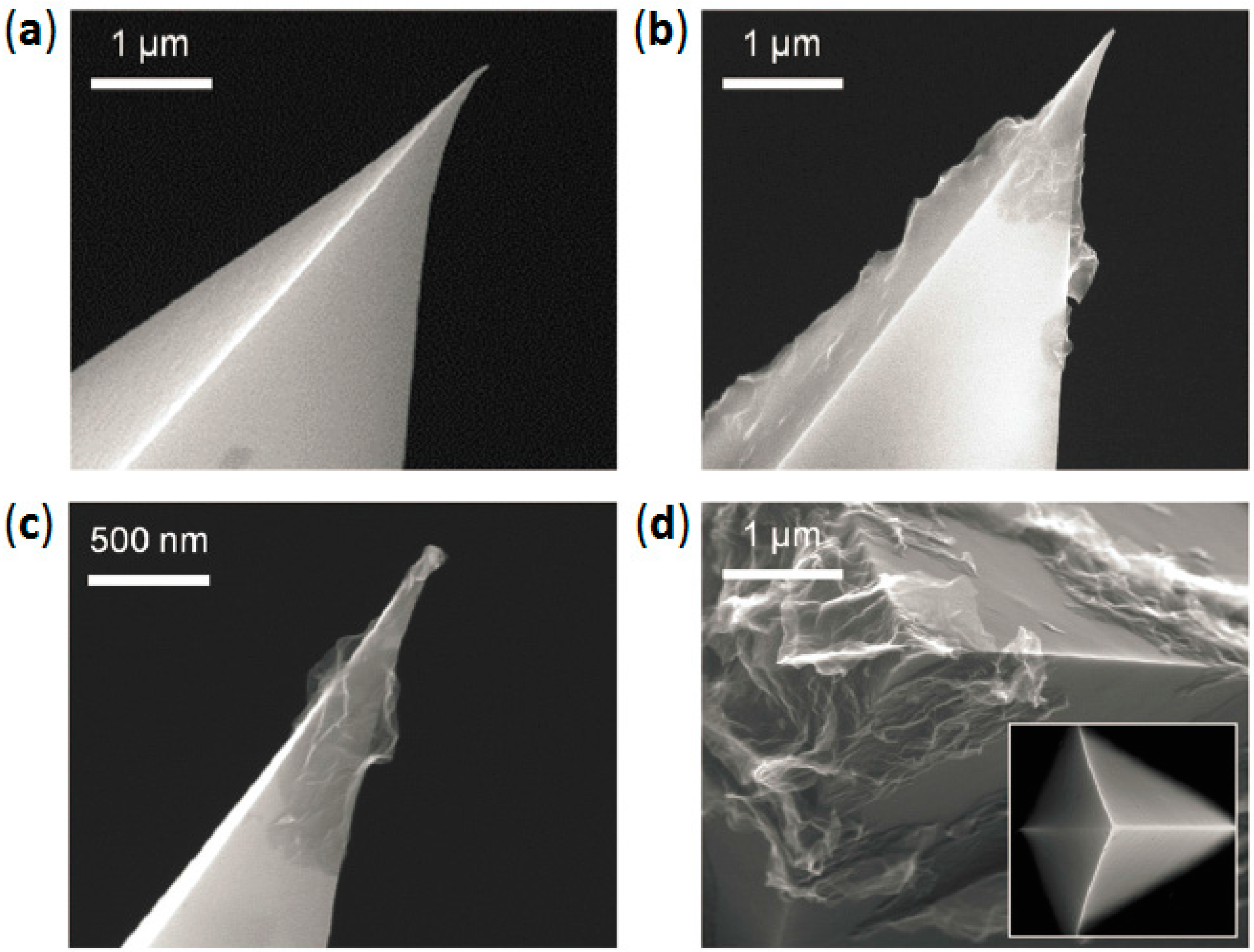
Figure 6.
Schematic illustration of standard AFM probes manufacturing by Nanoworld. (a) Silicon wafer with both sides of silicon dioxides; (b,d) exposure of the back and front sides to photoresist through a mask; (c,e) development of the exposed photoresist; (f) isotropic wet etching of silicon oxide; (g) dissolution of photo resist; (h,i) anisotropic wet etching of silicon by KOH and silicon oxide; (j–l) deposition and isotropic wet etching of silicon and silicon nitride, respectively. Reproduced with permission from [38], copyright Nanoworld 2008.

Figure 7.
As-fabricated AFM probes by Nanoworld manufacturer. (a) Wafer scale of AFM probes; SEM images of (b) as-fabricated AFM probes. Reproduced with permission from Ref. [38], copyright Nanoworld GmbH 2008; (c) Individual probe scratched by tweezers when picking it up. Reproduced with permission from [28], copyright The Royal Society of Chemistry (2016).

Figure 8.
Mechanical exploration of graphene coated AFM compared with uncoated ones. (a) Topographic images collected by both tapping mode and contact mode on the sample of Ag/SiO2. Reproduced with permission from [26], copyright American Chemical Society (2013); (b) 400 nm × 250 nm current maps of HfO2/SiO2 stack using a new (top) and worn-out commercial PtIr AFM conductive tip (bottom), the schematic in the right side represents the degree of wearing of tips; (c) SEM images indicate the degree of damage of the PtIr tip with and without graphene coating after use. The scale bars are 5 μm (left) and 3 μm (right), respectively. Reproduced with permission from [24], copyright Wiley-VCH (2013).
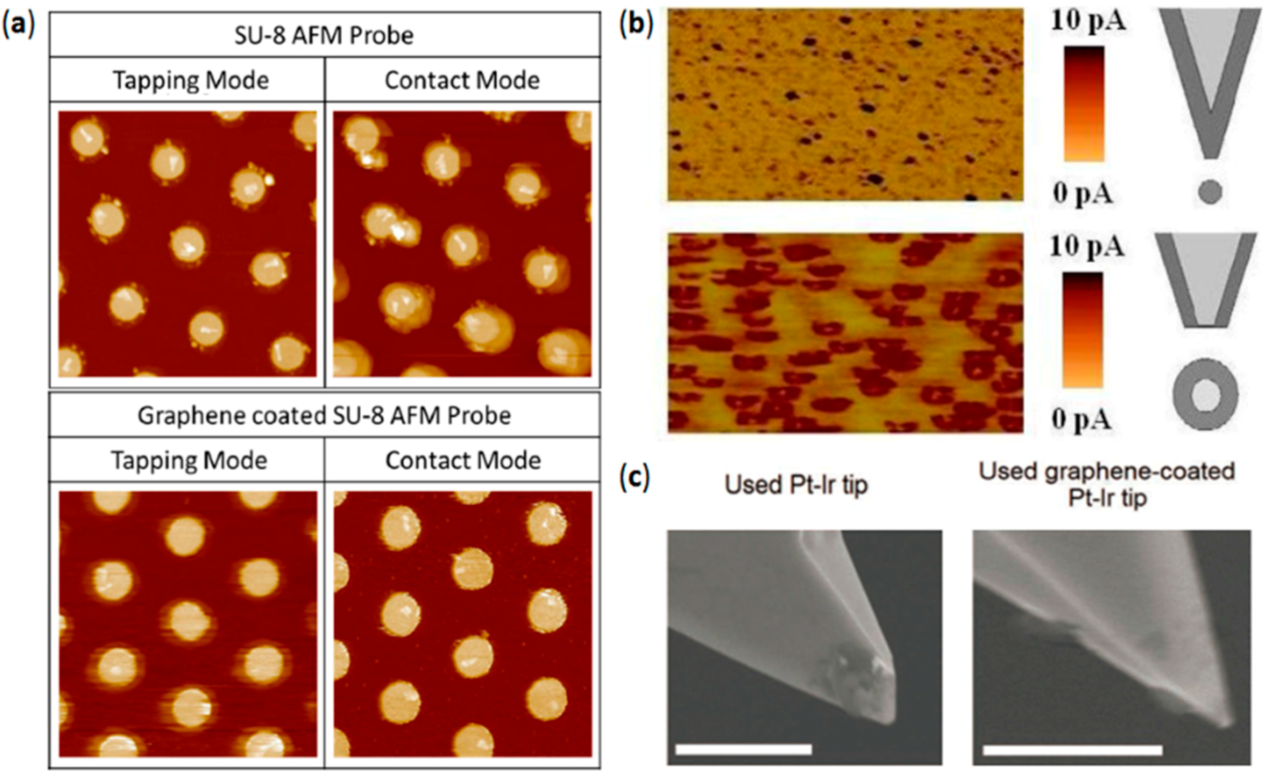
Figure 9.
Tip-sample interaction. Force-distance curves collected on Silicon substrate with a Pt coated AFM tip (a) and ultrathin graphite coated tip (b). Reproduced with permission from [27], copyright Springer Nature Publishing Group (2016); (c) Representative force-distance curves obtained by retracting a Si cantilever from a freshly-cleaved mica surface at different RH values that are listed next to each curve. Reproduced with permission from [43], copyright American Institute of Physics (2006); (d) Sequence of images collected at various relative humidity. The scale bars are 1 μm. Reproduced with permission from [42], copyright American Chemical Society (2005).

Figure 10.
(a) Typical forward and backward I–V curves collected with standard and graphene nanoprobes on a piece of n-type silicon; (b) Fitting of the forward and backward I–V curves collected with the standard tip to the charge transport model; 3D schematics of (c) standard and (d) graphene nanoprobe, which shows the water resistance of graphene. Reproduced with permission from [28], copyright The Royal Society of Chemistry (2016).

Figure 11.
Topographic (a,d) and current maps (b,e) recorded for as-received (top panel) and graphene-coated AFM tips (bottom panel) on 2.5 nm HfO2/Si stack; (c,f) Statistical analysis of the conductive spots are measured when scanning the surface of HfO2/SiO2/Si stack. Reproduced with permission from [29], copyright The Royal Society of Chemistry (2013).
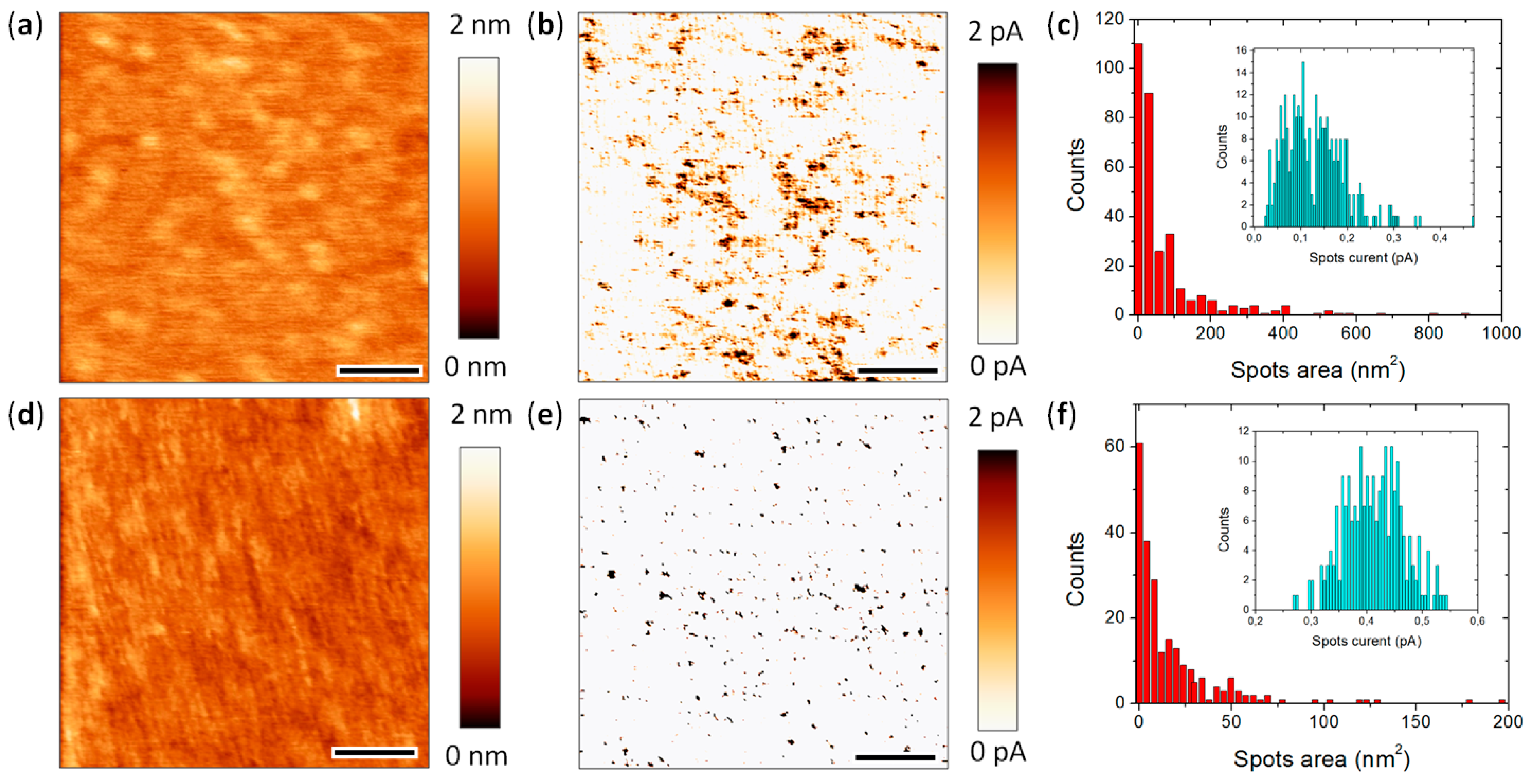
Figure 12.
Variability and stability test. (a) Average I-V data for Au/octanemonothiol/Au junctions with 18 different Au tips; (b) Average I-V data for Au/octanemonothiol/graphene/Au junctions with 18 different graphene tips. Reproduced with permission from [23], copyright Wiley-VCH (2012).
Figure 12.
Variability and stability test. (a) Average I-V data for Au/octanemonothiol/Au junctions with 18 different Au tips; (b) Average I-V data for Au/octanemonothiol/graphene/Au junctions with 18 different graphene tips. Reproduced with permission from [23], copyright Wiley-VCH (2012).

Figure 13.
100 backward I–V curves collected with both standard (a) and graphene coated nanoprobes; (b) the onset voltage and the deviation of the graphene nanoprobes is much smaller. Reproduced with permission from [28], copyright The Royal Society of Chemistry (2016); (c) Variance statistics analysis for single and multiple tip measurements at the saturation voltage (I = −5 nA) for fresh probes (in red) or graphene coated (in blue). Reproduced with permission from [52], copyright Elsevier (2016).
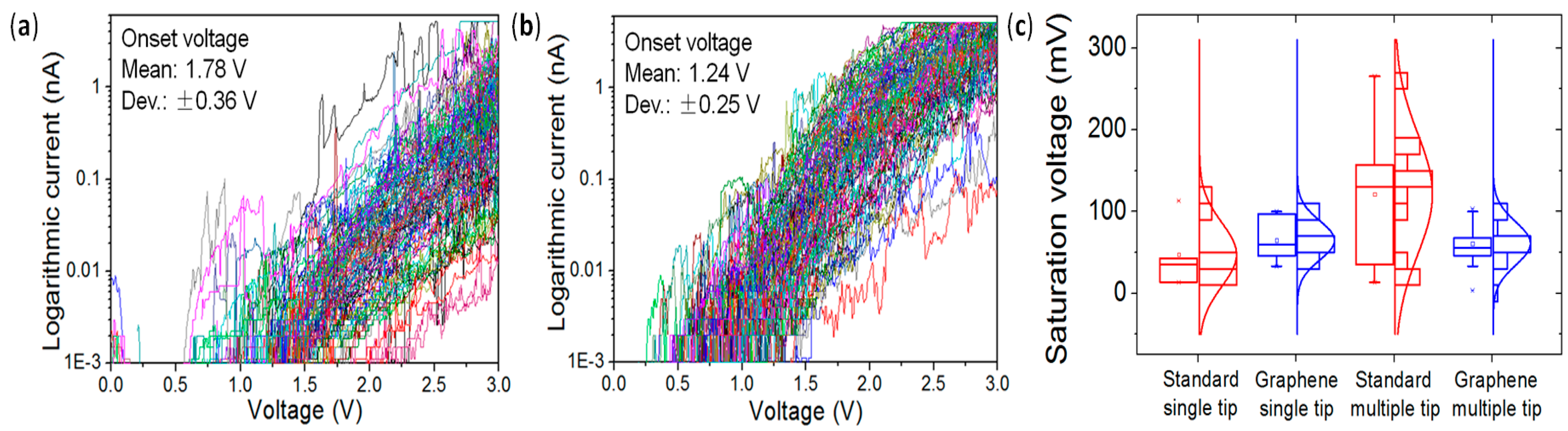
Figure 14.
Reliability and durability test. Current vs. Voltage (I–V) curves performed on different positions of HfO2/Si stack by (a) uncoated AFM tip and (d) graphene coated tips. Reproduced with permission from [24], copyright Wiley-VCH (2013). Current spectra and the insets in (b) are the 1st (blue) and 13th (red) CAFM current maps collected on graphene/Cu foil with a standard metal-varnished nanoprobe. Current spectra and the insets in (e) are the 1st (blue) and 92th (red) CAFM current maps collected with a graphene coated nanoprobe. SEM images of AFM tips without (c) and with graphene coating (f) after testing. Reproduced with permission from [28], copyright The Royal Society of Chemistry (2015).


Table 1.
Specifications of the most used commercial conductive nanoprobes from different manufacturers. The prices represent the cost given by the local distributors in Shanghai.
Table 1.
Specifications of the most used commercial conductive nanoprobes from different manufacturers. The prices represent the cost given by the local distributors in Shanghai.
| Type | Model | Tip Coating (nm) | Bulk Materials | Tip Radius (nm) | Spring k (N/m) | Freq (kHz) | Manufacturer | Unit Price ($) |
|---|---|---|---|---|---|---|---|---|
| Metal varnished Si tip | SCM-PIC | PtIr | n-doped Si | 20 + 5 | 0.2 (0.1–0.4) | 13 (10–16) | Bruker | 41.9 |
| OSCM-PT | Pt (20) | Si | 15 + 10 | 2 (0.6–3.5) | 70 (50–90) | Bruker | 51.2 | |
| SCM-PTSI | Pt/Si | n-doped Si | 15 + 10 | 2.8 (1–5) | 75 (50–100) | Bruker | 156.7 | |
| SMIM-150 | TiW | Si3N4 | 50 ± 10 | 8 (7–9) | 75 (70–80) | Bruker | 139.8 | |
| MESP | Co/Cr | Si | 35 + 15 | 2.8 (1–5) | 75 (50–100) | Bruker | 116.7 | |
| Arrow CONTPT | Cr/PtIr (5/25) | Si | 33 ± 10 | 0.2 (0.06–0.38) | 14 (10–19) | NanoWorld | 38 | |
| CONTPT | Cr/PtIr (5/25) | Si | 30 ± 10 | 0.2 (0.07–0.4) | 13 (9–17) | NanoWorld | 42.98 | |
| ATEC-CONTPT | Cr/PtIr (5/25) | Si | 33 ± 10 | 0.2 (0.02–0.75) | 15 (7–25) | Nanosensors | 41.39 | |
| PPP-CONTPT | Cr/PtIr (5/25) | Si | 30 ± 10 | 0.2 (0.02–0.77) | 13 (6–21) | Nanosensors | 46.11 | |
| PtSi-NCH | Pt | Si | 30 ± 10 | 42 (10–130) | 330 (204–497) | Nanosensors | 152.08 | |
| ACCESSS-NC-GG | Au | Si | 30 | 113 | 330 | App Nano | 53.99 | |
| TiN-ACT | TiN | Si | 70 | 37 | 300 | App Nano | 39.5 | |
| AC240TM | Ti/Pt (5/20) | Si | 28 ± 10 | 2 (0.3–4.8) | 70 (45–95) | Olympus | 35.94 | |
| NSC14/Pt | Pt or Au | Si | <30 | 5 (1.8–13) | 160 (110–220) | μ-Masch | 40.3 | |
| Electri Tap 190-G | Cr/Pt | Si | <25 | 48 (20–100) | 190 ± 60 | Budgetsensors | 37.26 | |
| Doped diamond varnished Si tip | CDT-FMR | Doped diamond | Si | 83 ± 17 | 2.8 (1.2–5.5) | 75 (60–90) | NanoWorld | 143.66 |
| CDT-CONTR | Doped diamond | Si | 83 ± 17 | 0.2 (0.02–0.77) | 13 (6–21) | Nanosensors | 152.08 | |
| CDT-NCLR | Doped diamond | Si | 83 ± 17 | 48 (21–98) | 190 (146–236) | Nanosensors | 152.08 | |
| DD-ACCESS-NC | Doped diamond | Si | 100–300 | 93 | 320 | App Nano | 154.48 | |
| DDESP-FM | Doped diamond | Si | 150 + 50 | 6.2 (3–11.4) | 105 (80–103) | Bruker | 132.8 | |
| AD-0.5-AS | Single crystal diamond | Si | 10 ± 5 | 0.5 (0.1–1) | 30 (10–50) | Bruker | 186.5 | |
| AD-0.5-SS | Single crystal diamond | Si | <5 | 0.5 (0.1–1) | 30 (10–50) | Bruker | 279.6 | |
| Solid metal AFM tip | RMN-12PT400B | None | Pt | 15 ± 5 | 0.3 (0.18–0.42) | 4.5 (3.15-5.85) | Bruker | 74.5 |
| Solid doped diamond AFM tip | SSRM-DIA | None | Diamond | 5–20 | 3/11/27 | - | Bruker (IMEC) | 372.2 |
| P-CT1T2S | None | Diamond | - | 0.71 | 50 | Advanced Creative Solution Technology | 1050 | |
| P-CTCR1S | None | Diamond | <10 nm | 0.35 | 35 | Advanced Creative Solution Technology | 950 |
© 2017 by the authors. Licensee MDPI, Basel, Switzerland. This article is an open access article distributed under the terms and conditions of the Creative Commons Attribution (CC BY) license (http://creativecommons.org/licenses/by/4.0/).
Share and Cite
MDPI and ACS Style
Hui, F.; Chen, S.; Liang, X.; Yuan, B.; Jing, X.; Shi, Y.; Lanza, M. Graphene Coated Nanoprobes: A Review. Crystals 2017, 7, 269. https://doi.org/10.3390/cryst7090269
AMA Style
Hui F, Chen S, Liang X, Yuan B, Jing X, Shi Y, Lanza M. Graphene Coated Nanoprobes: A Review. Crystals. 2017; 7(9):269. https://doi.org/10.3390/cryst7090269
Chicago/Turabian StyleHui, Fei, Shaochuan Chen, Xianhu Liang, Bin Yuan, Xu Jing, Yuanyuan Shi, and Mario Lanza. 2017. "Graphene Coated Nanoprobes: A Review" Crystals 7, no. 9: 269. https://doi.org/10.3390/cryst7090269
Note that from the first issue of 2016, this journal uses article numbers instead of page numbers. See further details here.