1. Introduction
Photonic crystals (PCs) are one-dimensional (1D), two-dimensional (2D), or three-dimensional (3D) ordered structures with a periodicity comparable to an optical wavelength. They are composed of two or more different dielectrics and their periodicity opens up a photonic band gap (PBG) in which the existence of photons is forbidden [
1,
2]. This can be explained by an analogy of electrons in a solid-state crystal. In a PBG, electromagnetic fields cannot propagate due to destructive interference between waves scattered from the periodically modulated refractive index structure. This fact is similar to the destructive interference of electron waves from a periodic potential of an atomic lattice in a certain frequency. PCs have attracted considerable attention from both fundamental and practical points of view because various applications of PCs have been proposed [
3,
4,
5,
6,
7].
Tunable PCs have been proposed by using opals or inverse opals infiltrated with liquid crystal (LC) having optical anisotropy and field sensitivity [
8,
9,
10,
11,
12]. LCs are mesophases between crystalline solids and isotropic liquids. They may flow like viscous fluids and also possess features that are characteristic of solid crystals. The constituents are rod-like or disk-like organic molecules which normally have self-assembled characteristics. These molecules exhibit different physical properties between the long and short molecular axes. Consequently, LCs have various anisotropies, such as permittivity, refractive index, and viscosity. We can control the molecular director by application of an electric field because the fluidity and dielectric anisotropy allow LC molecules to align parallel or perpendicular to the electric field. Such a change of molecular orientation allows us to control the optical properties of a LC-filled PC because optical properties of PCs are determined by refractive index modification.
When there is a defect that disturbs the periodicity of a PC, localized photonic states appear in a PBG. The states are so-called defect modes at which photons are confined in the defect. In particular, 3D PBG materials with a defect allow us to achieve a 3D photon confinement. Such an optical confinement is the most important feature of PCs because an electric field in a defect can be strongly enhanced at a defect mode resonance frequency. An appropriate line defect in a 2D or 3D PC serves as a waveguide that can guide light in a desired direction by PBG confinement [
13,
14]. Such a defect acting as a microcavity or a waveguide is very important in certain applications, such as low-threshold lasers, micro-waveguides, and optical circuits [
13,
14,
15,
16,
17,
18,
19].
Tunable defect modes are also an attractive subject. However, the introduction of a defect in a 3D PC using a nano-fabrication remains a major technical challenge [
14]. Although 1D PCs do not have a complete PBG, there are plenty of applications using an extraordinary wavelength dispersion and a localized photonic state in a defect layer. So far, intensive studies on 1D PC applications have been reported: air-bridge microcavities [
20,
21], photonic band-edge lasers [
17], nonlinear optical diodes [
22], and enhancements of optical nonlinearity [
23,
24]. We have studied a nematic LC (NLC) layer in a dielectric multilayer as a defect in a 1D PC [
25,
26,
27,
28], in which the wavelengths of defect modes were controlled upon applying an electric field based on a change in the optical length of the defect layer caused by field-induced molecular reorientation of the NLC. Furthermore, the modulation of defect mode lasing [
25] and the high speed electrooptic switching [
26,
27] upon applying a low voltage have been demonstrated by using a 1D PC containing an NLC defect layer. Recently, some interesting concepts have been reported using various LC defects in a 1D PC [
29,
30,
31,
32]. In this paper, we investigate polarization characteristics of defect mode peaks in a 1D PC with an NLC defect. The polarization control at the defect mode wavelength is demonstrated by in-plane reorientation of the NLC defect layer. Furthermore, the finite difference time domain (FDTD) simulation is also performed to investigate the polarization of transmitted light from the 1D PC with the NLC defect.
3. Results and Discussion
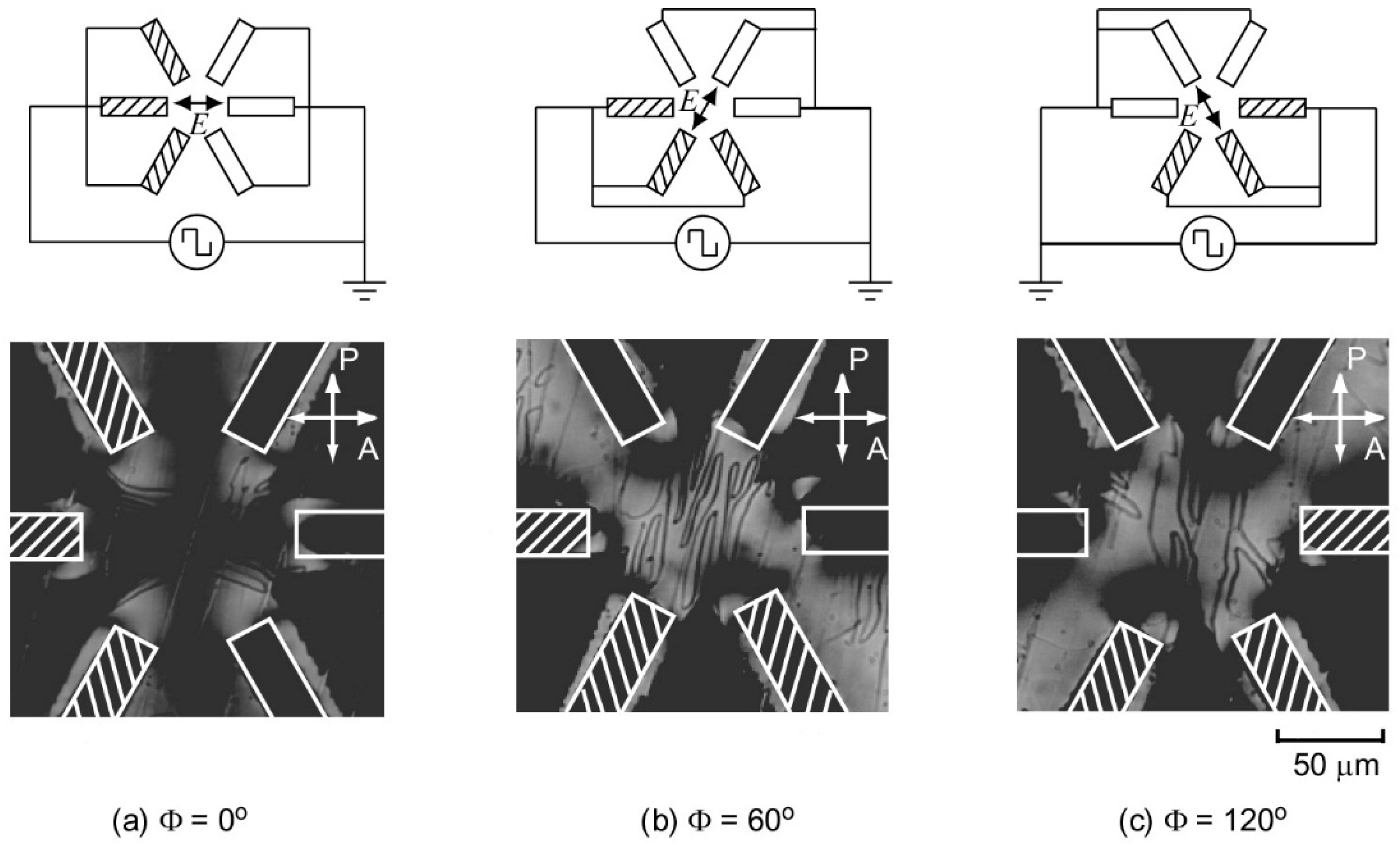
Polarization microscope images of the NLC defect layer are shown in
Figure 2a–c, where we used the circuits to apply a voltage to the six electrodes. The angle Φ represents the direction of an applied electric field. Under no electric field, the NLC molecules in the defect layer aligned homeotropically because the NLC layer at 0 V was always dark despite rotating the cell on the microscope stage. In
Figure 2a–c, a rectangular wave voltage of 200 V with a frequency of 1 kHz was applied between hatched and non-hatched electrodes. In this system, Φ can be controlled by adjusting positions of the potential applied to six electrodes. When the electric field was applied along Φ = 0° as shown in
Figure 2a, the NLC director aligned parallel to Φ = 0°. Under the condition, the NLC at the center of the electrodes was in a dark state because the NLC director was parallel to the analyzer. In contrast, in
Figure 2b,c, the NLC aligned along Φ = 60° and Φ = 120°, and then a bright state was obtained. From these results, we confirmed that the NLC director in the defect layer was able to be electrically controlled.
Figure 2.
Polarization microscopic images of the NLC defect layer upon applied electric field for (a) Φ = 0°, (b) Φ = 60°, and (c) Φ = 120°. Illustrated circuits were used to apply a voltage to the six electrodes.
Figure 2.
Polarization microscopic images of the NLC defect layer upon applied electric field for (a) Φ = 0°, (b) Φ = 60°, and (c) Φ = 120°. Illustrated circuits were used to apply a voltage to the six electrodes.
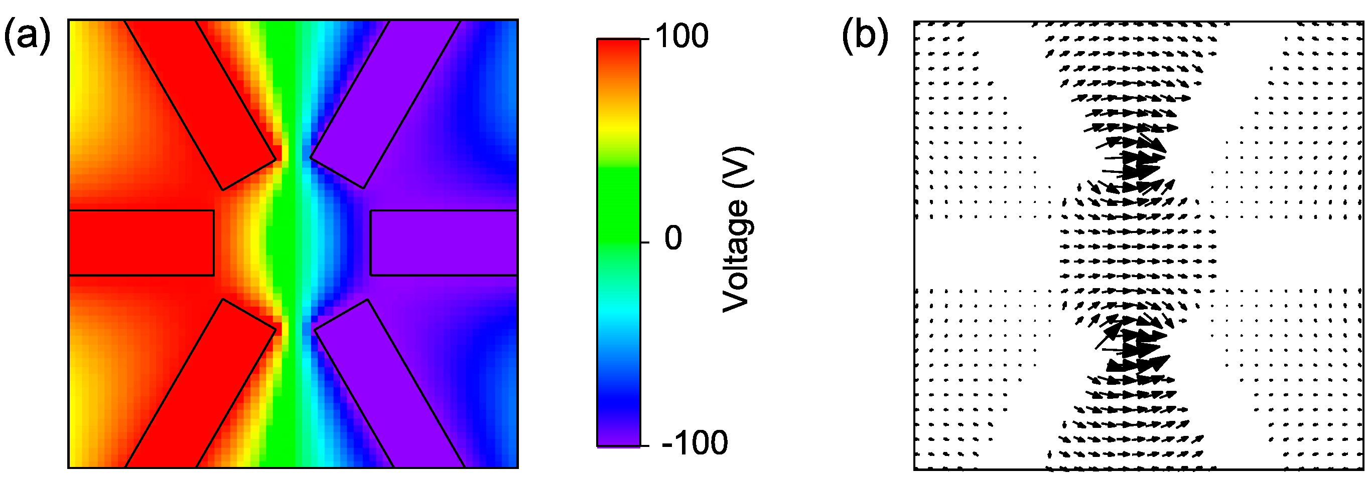
Furthermore, we also performed a numerical calculation of an electric field in the defect layer using a finite differential method to investigate details of NLC directors. In this calculation, the calculated area of the defect layer was composed of 100 × 100 grid alignments. Since the electric field was mainly applied to the center of six electrodes, the potential of the boundary far away from electrodes was set to be zero. To obtain potentials at all grids, we numerically solved Laplace’s equation using an iterative method.
Figure 3a shows the calculated potential profile when a rectangular wave voltage of 200 V was applied between hatched and non-hatched electrodes shown in
Figure 2a. Here, the potential profile shows only the center area. The calculated electric field vectors are shown in
Figure 3b in which arrow size and direction represent the magnitude and the direction of the electric field, respectively. We here consider that NLC directors align parallel to arrows because Δε is positive. Under a crossed Nicols condition, when NLC directors are parallel to the polarizer or analyzer, a dark state is obtained in a polarization microscopic image. Note that arrows parallel to the polarizer or analyzer correspond to dark states in
Figure 2a. In contrast, arrows not parallel to the polarizer or analyzer correspond to bright states. These calculations explain the experimental result shown in
Figure 2a. Therefore, the orientation of the NLC in the defect layer was also confirmed theoretically.
Figure 3.
(a) Calculated potential in the NLC defect layer obtained by applying a rectangular voltage of 200 V with Φ = 0°; (b) Calculated electric field vectors in the NLC defect layer.
Figure 3.
(a) Calculated potential in the NLC defect layer obtained by applying a rectangular voltage of 200 V with Φ = 0°; (b) Calculated electric field vectors in the NLC defect layer.
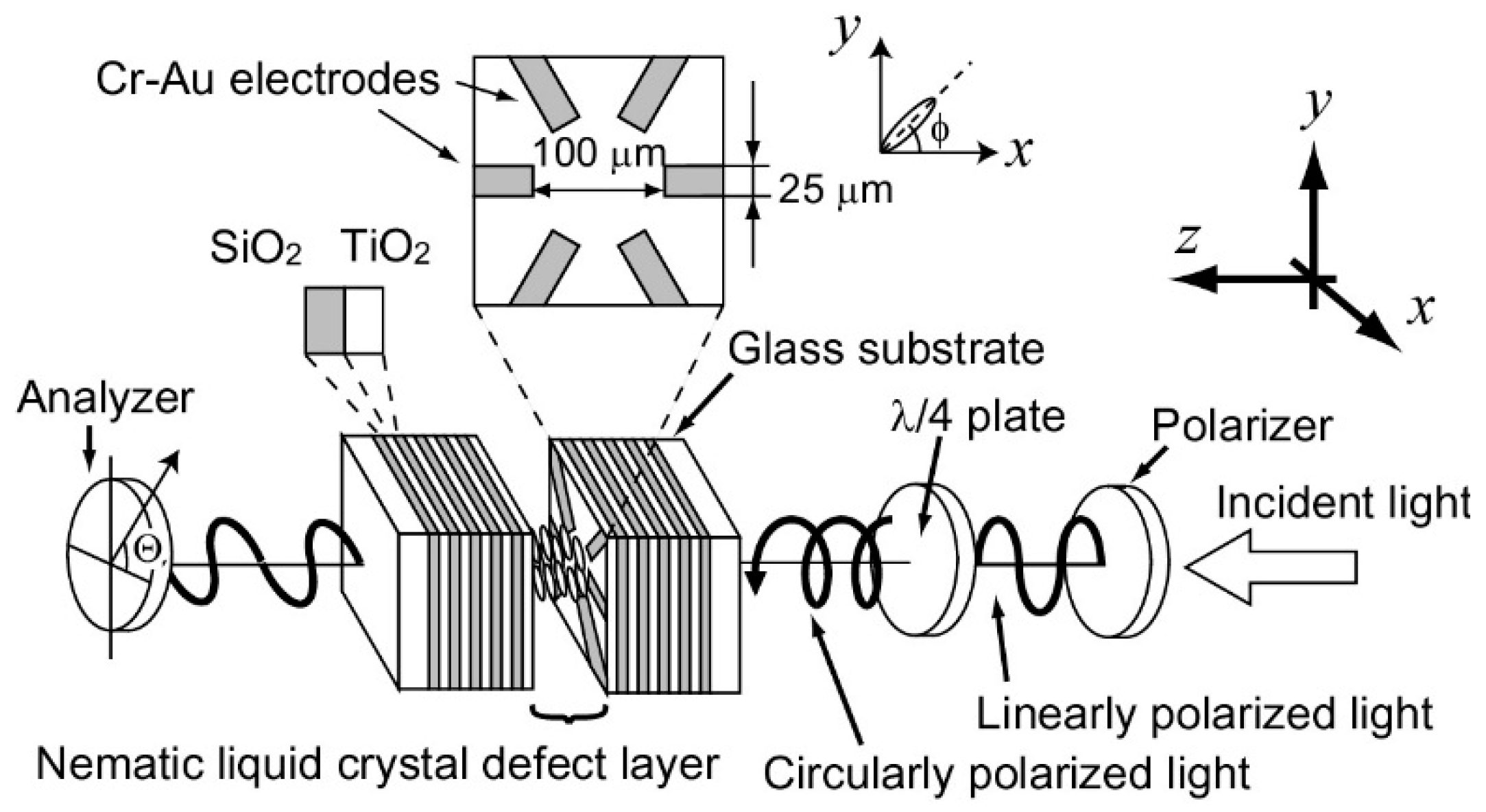
We measured transmission spectra of the 1D PC with the NLC defect after the polarization microscopic observations. Incident light was circularly polarized and was obtained by placing a λ/4 plate after the polarizer, as shown in
Figure 1. To investigate polarization characteristics of transmitted light, the analyzer was rotated in the transmission measurements.
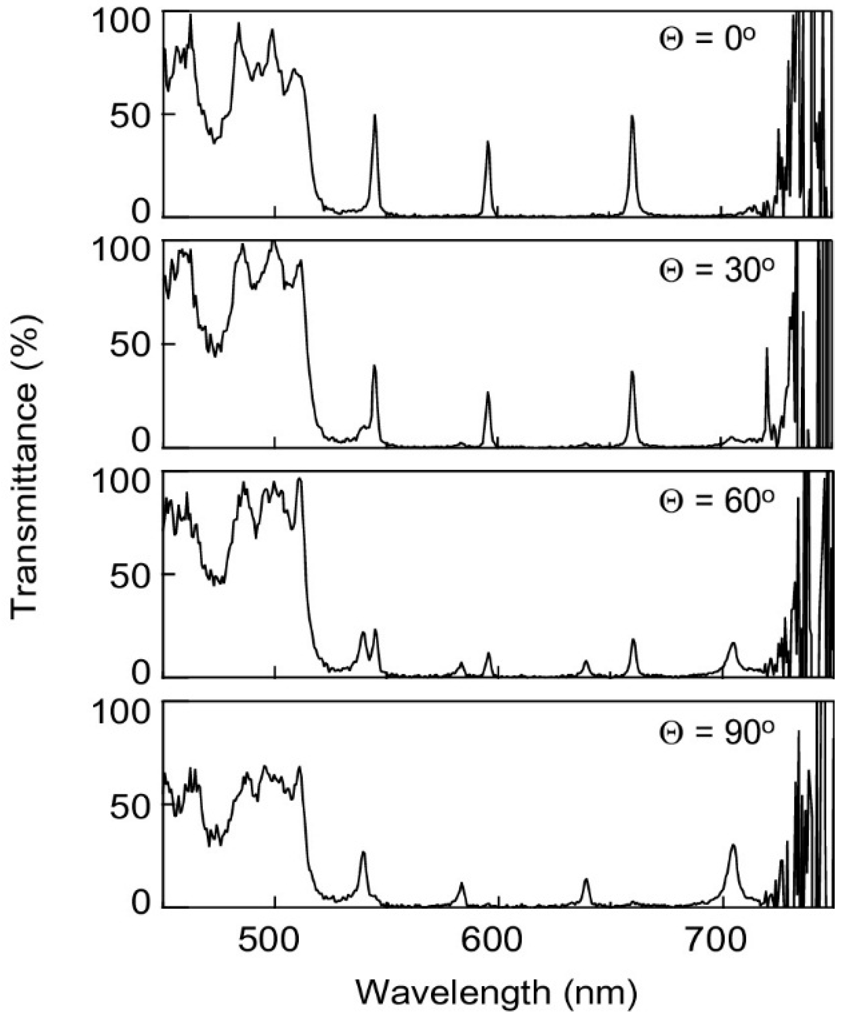
Figure 4 shows transmission spectra of the 1D PC with the NLC defect at Φ = 0° as a function of analyzer angle Θ.
Figure 4.
Transmission spectra of the 1D PC with the NLC defect for analyzer angles: Θ = 0°, 30°, 60°, and 90°.
Figure 4.
Transmission spectra of the 1D PC with the NLC defect for analyzer angles: Θ = 0°, 30°, 60°, and 90°.
Note that some peaks appeared in the PBG of the 1D PC which were observed in the spectral range from 530 to 750 nm. These peaks were caused by defect modes induced by the introduction of the NLC defect layer. It is clear that intensities of the defect mode peaks depend on Θ. At Θ = 0°, three peaks appeared at 545, 595, and 660 nm. The peak intensities decreased with the rotating analyzer from Θ = 0° to 90°, and then another four peaks at 540, 583, 640, and 705 nm appeared in the PBG. Regardless of entering circularly polarized light, intensities of the transmitted lights propagating through the 1D PC with the NLC defect depended on Θ. These results indicate that transmitted lights at defect mode wavelengths are polarized to a certain direction.
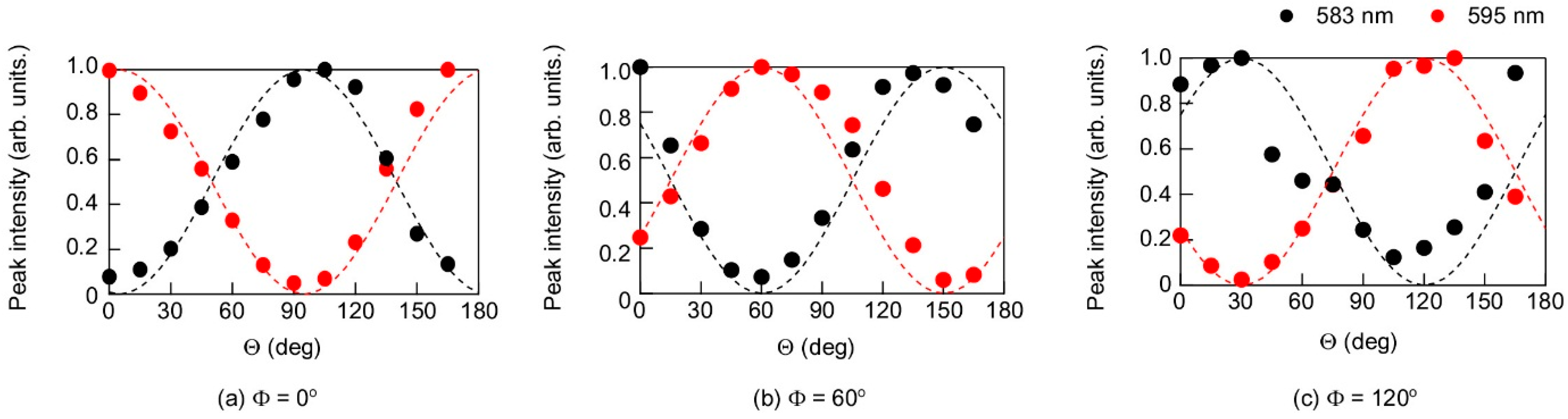
To investigate the details of the polarization characteristics, we plotted peak intensities of the defect modes.
Figure 5 shows polarization characteristics of the transmitted light through the 1D PC with the NLC defect for Φ = 0°, 60°, and 90°. Red and black broken lines are sin
2(Θ − Φ) and cos
2(Θ – Φ), respectively, and the experimental data fits the curves well. Note that the maximum values of defect mode peaks for 595 and 583 nm approximately appear at Θ = Φ and Θ = Φ + 90°, respectively. This means that transmitted lights at defect mode wavelengths are polarized along the long or short axis of the NLC molecules. In other words, the defect modes are associated with the extraordinary and ordinary refractive indices of the NLC molecules in the defect layer. The phenomenon can be explained as follows. The incident light induces a dipole moment along the short and the long molecular axes. The dipole moment is the origin of the polarization of light. In a PBG, dipole radiation is suppressed, except at a defect mode wavelength. Optical conditions for forming a defect mode are different between ordinary and extraordinary modes. Therefore, the transmitted light at a defect mode wavelength will have a linear polarization parallel to the short or the long molecular axis.
Figure 5 also indicates that the polarization of the transmitted light can be controlled by changing the applied electric field direction. On the other hand, it is demonstrated from the theoretical calculation that the electric field in the defect layer can be controlled in any direction upon arranging the distribution of an applied voltage to the electrodes.
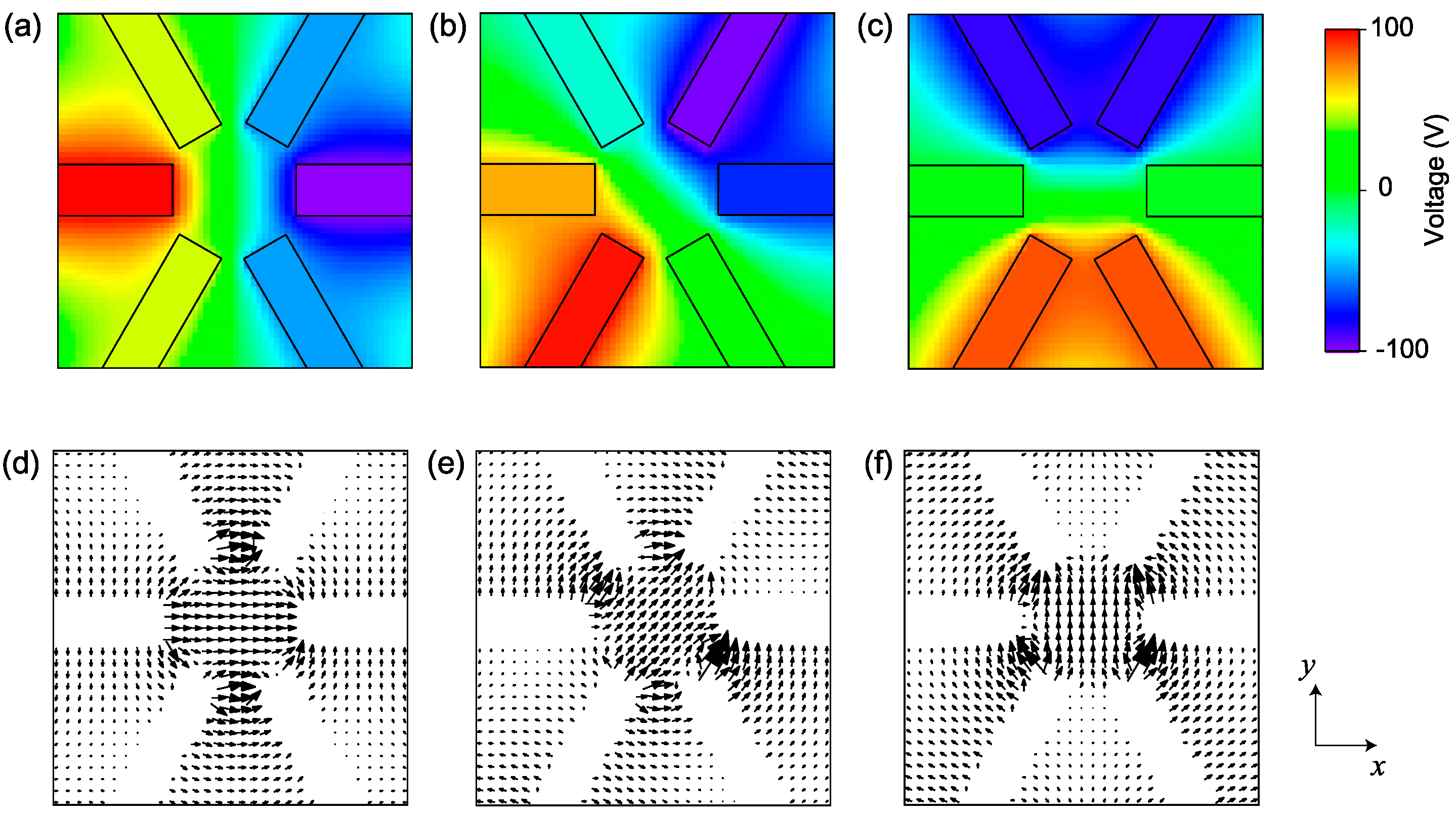
Figure 6 shows calculated potentials and electric fields in the defect layer when three-phase AC voltage (three phases A, B, and C) are applied.
Figure 6a,d are snapshots of the potential of the three-phase AC voltage at phase A = 0° and its electric field, respectively. The electric field vectors at the center of the six electrodes were parallel to the
x-axis. In contrast, the electric field vectors at the center area in
Figure 6e orient with an angle of 45° from the
x-axis. The difference between
Figure 6d,e is caused by the phase angle of the voltage. Similarly,
Figure 6f shows electric field vectors parallel to the
y-axis at the center area. From these results, we consider that the 1D PC with the NLC defect is expected to be a candidate for an optical rotator [
33,
34,
35].
Figure 5.
Polarization characteristics of the defect mode peaks at 583 and 595 nm in the 1D PC with the NLC defect for three applied electric field directions: (a) Φ = 0°, (b) Φ = 60°, and (c) Φ = 120°.
Figure 5.
Polarization characteristics of the defect mode peaks at 583 and 595 nm in the 1D PC with the NLC defect for three applied electric field directions: (a) Φ = 0°, (b) Φ = 60°, and (c) Φ = 120°.
Figure 6.
Snapshots of calculated potential in the NLC defect layer obtained by applying three-phase AC voltage: (a) Phase A = 0°, (b) Phase A = 45°, and (c) Phase A = 90°. Calculated electric field vectors at (d) Phase A = 0°, (e) Phase A = 45°, and (f) Phase A = 90°.
Figure 6.
Snapshots of calculated potential in the NLC defect layer obtained by applying three-phase AC voltage: (a) Phase A = 0°, (b) Phase A = 45°, and (c) Phase A = 90°. Calculated electric field vectors at (d) Phase A = 0°, (e) Phase A = 45°, and (f) Phase A = 90°.
We also performed numerical calculations of the light propagation through the 1D PC with the NLC defect using the FDTD method. The FDTD calculation is an analysis of the Maxwell equations according to the Yee algorithm in discrete time and lattices [
36].
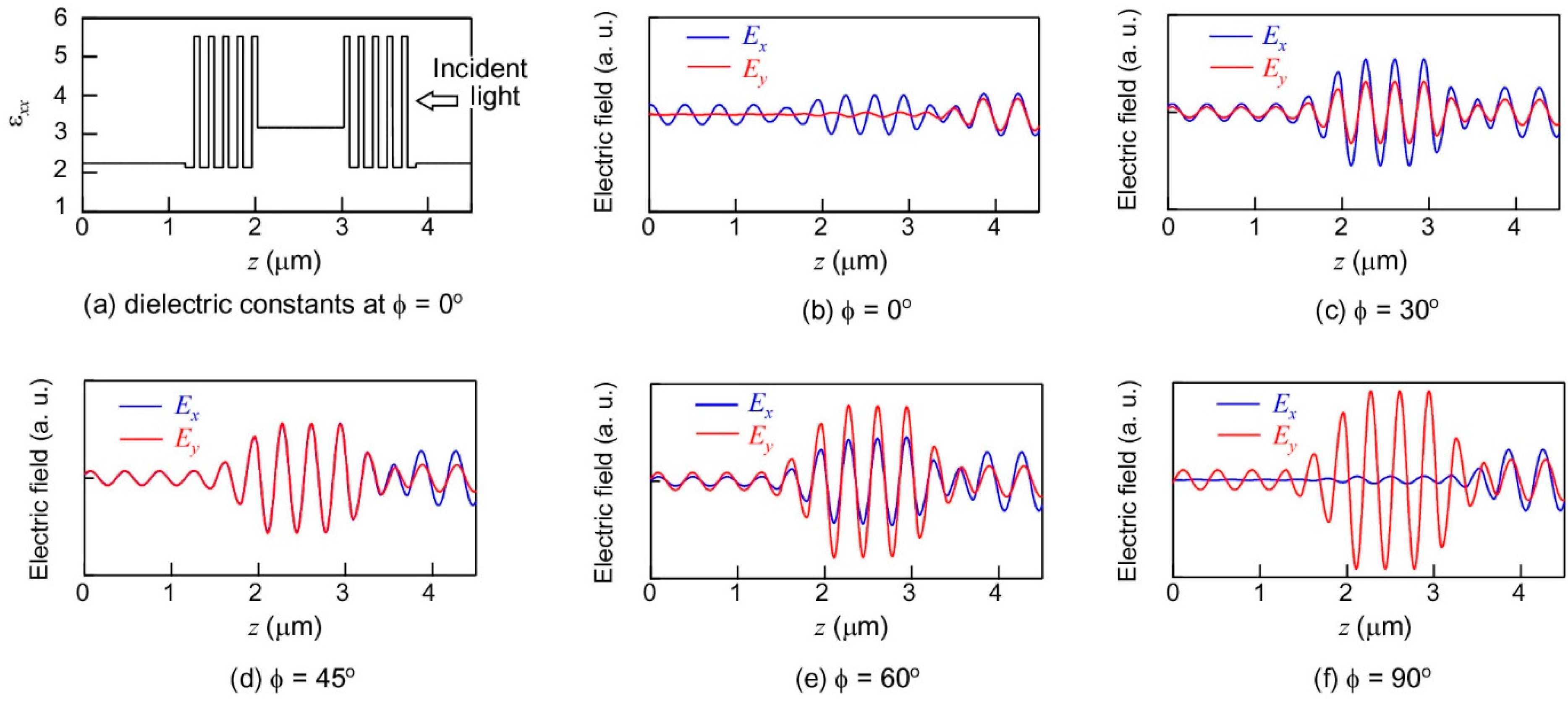
Figure 7a shows the profile of ε
xx of the 1D PC with the NLC defect at ϕ = 0°, where ϕ is an azimuthal angle of the NLC molecules in the defect layer as shown in
Figure 1.
Figure 7.
Calculated structure of the 1D PC with the NLC defect: (a) εxx profile at ϕ = 0°. Electric field profiles of Ex and Ey propagating through the 1D PC with the NLC defect at a wavelength of 595 nm: (b) ϕ = 0°, (c) ϕ = 30°, (d) ϕ = 45°, (e) ϕ = 60°, and (f) ϕ = 90°.
Figure 7.
Calculated structure of the 1D PC with the NLC defect: (a) εxx profile at ϕ = 0°. Electric field profiles of Ex and Ey propagating through the 1D PC with the NLC defect at a wavelength of 595 nm: (b) ϕ = 0°, (c) ϕ = 30°, (d) ϕ = 45°, (e) ϕ = 60°, and (f) ϕ = 90°.
We used physical parameters of this structure described in
Section 2. In this calculation, the circularly polarized light with a wavelength of 595 nm was entered to the 1D PC with the NLC defect along the
z-axis, and the NLC defect layer was placed in the region from
z = 2 to 3 μm. The first-order Mur’s absorbing boundary condition was used at the boundaries of the system.
Figure 7b–f shows electric field profiles of
Ex and
Ey propagating through the 1D PC with the NLC defect. The polarization of transmitted light can be estimated from the difference between
Ex and
Ey at the output side. In
Figure 7b,
Ex propagates through the 1D PC with the NLC defect, whereas
Ey is hardly transmitted. When the NLC director aligns to ϕ = 45°, amplitudes of
Ex and
Ey become equal as shown in
Figure 7d. At ϕ = 90°,
Ex is hardly transmitted, whereas
Ey propagates through the 1D PC with the NLC defect. Another important fact is that
Ex and
Ey are almost in phase. This indicates that the polarization of the transmitted light from the 1D PC with NLC defect is linear.
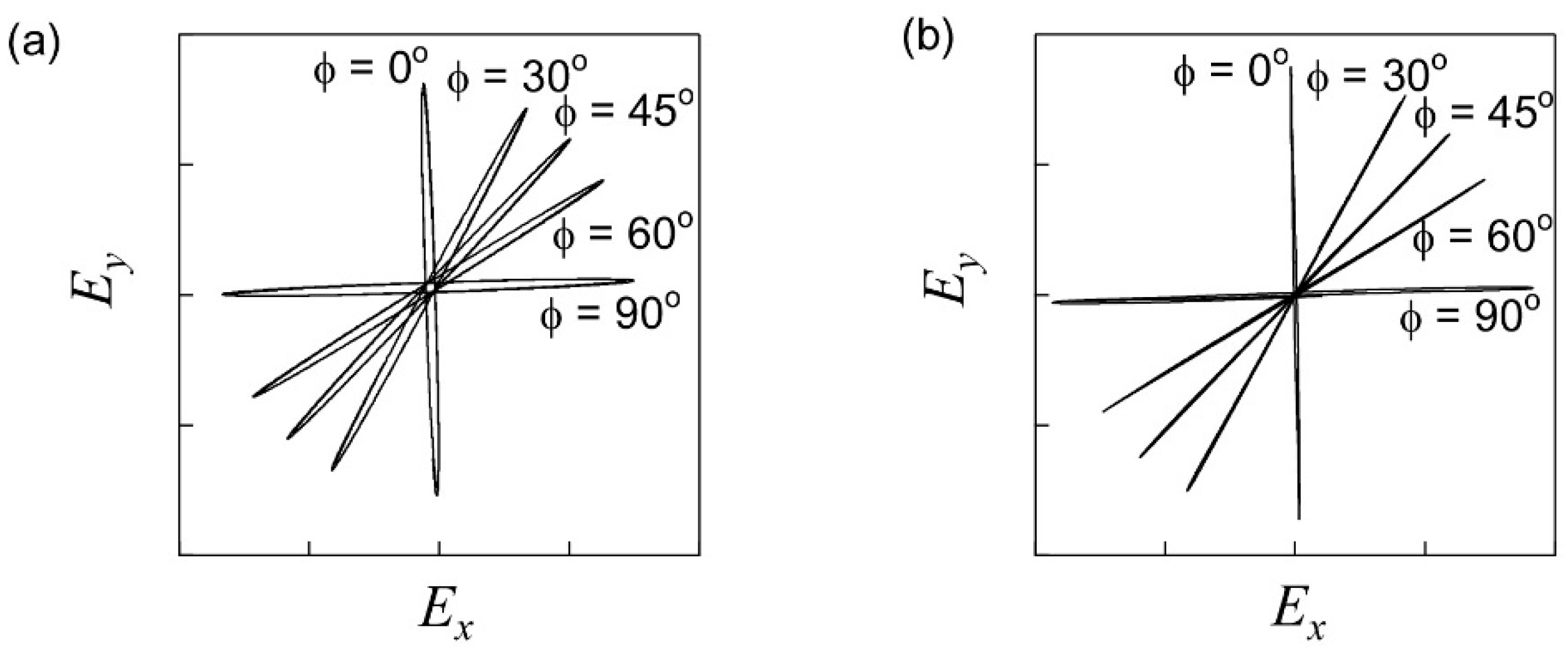
Let us see the calculated transmitted light from a different angle.
Figure 8a shows calculated polarization characteristics of the transmitted light propagating through the 1D PC with the NLC defect. In this graph, the transmitted
Ex and
Ey are plotted in the
xy-plane. Note that the polarizations of the transmitted light are varied by rotating NLC molecules in the defect. Furthermore, the polarization angles agree with ϕ. However, the calculated transmitted light polarization is shown a little bit elliptically. Ellipticity defined by the elliptic short axis divided by the long axis is 0.04. In this case, the polarization extinction ratio at the wavelength is 625:1. This result is caused by the fact that the ten-period 1D PC does not have enough periodicity to forbid other components.
Figure 8b shows the polarization of the 16-period 1D PC with the NLC defect which has stronger suppression in the PBG. As is evident from this figure, characteristics of the polarization propagating through the 16-period 1D PC with the NLC defect are sharper. Ellipticity of the 16-period 1D PC with the NLC defect is 0.01, and the polarization extinction ratio becomes 10000:1. The output polarizations of ϕ = 0° and ϕ = 90° are not exactly vertical or horizontal. This is because transmitted light and leaked light are not in phase. From the FDTD calculations we found that the polarization of transmitted light from the system was linear and parallel to ϕ and that the linearity depends on the number of periods of the 1D PC.
Figure 8.
Calculated transmitted light propagating through the 1D PC with the NLC defect at a wavelength of 595 nm as a function of ϕ. The numbers of periods of 1D PC are (a) 10 and (b) 16.
Figure 8.
Calculated transmitted light propagating through the 1D PC with the NLC defect at a wavelength of 595 nm as a function of ϕ. The numbers of periods of 1D PC are (a) 10 and (b) 16.

