Metals on Graphene: Interactions, Growth Morphology, and Thermal Stability


Abstract
:
1. Introduction
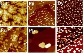
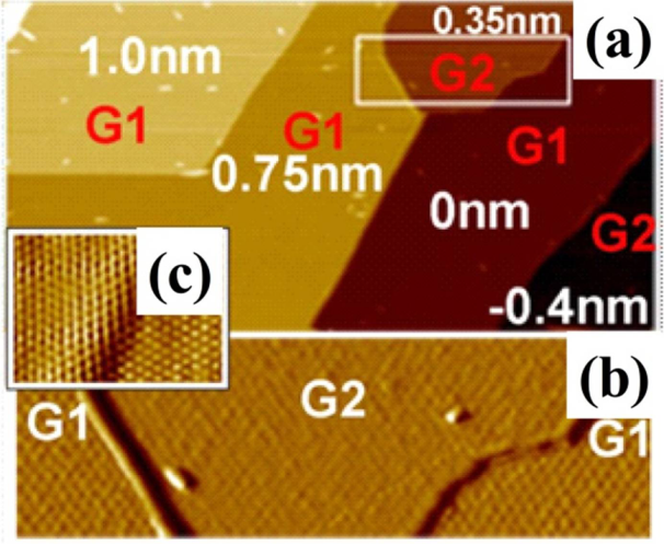
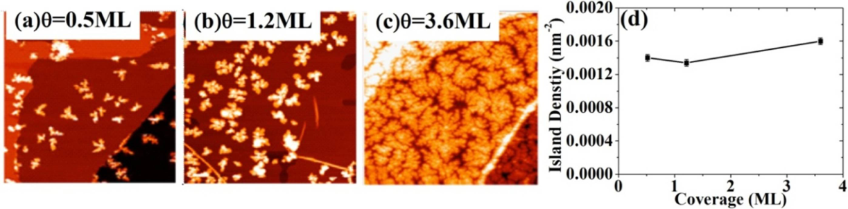
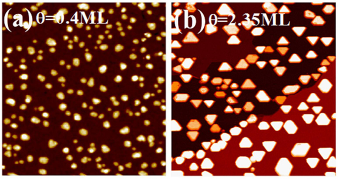
2. Growth Morphology of Metal on Graphene

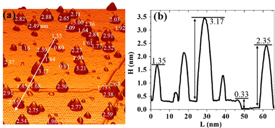
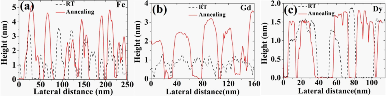
2.1. Gd on Graphene

2.2. Dy on Graphene

2.3. Eu on Graphene
2.4. Fe on Graphene


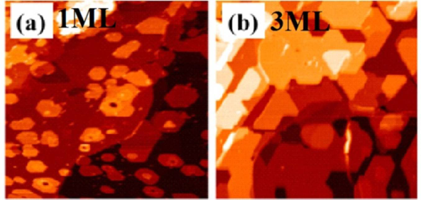
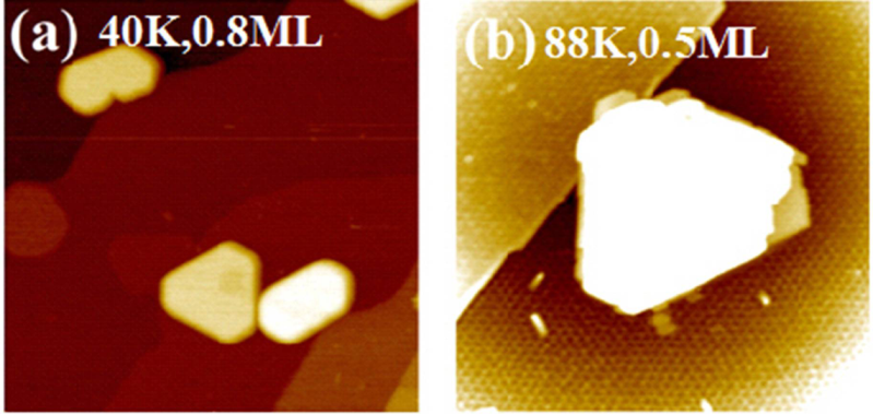
2.5. Pb on Graphene
3. Interactions between Metal Adatoms and Graphene
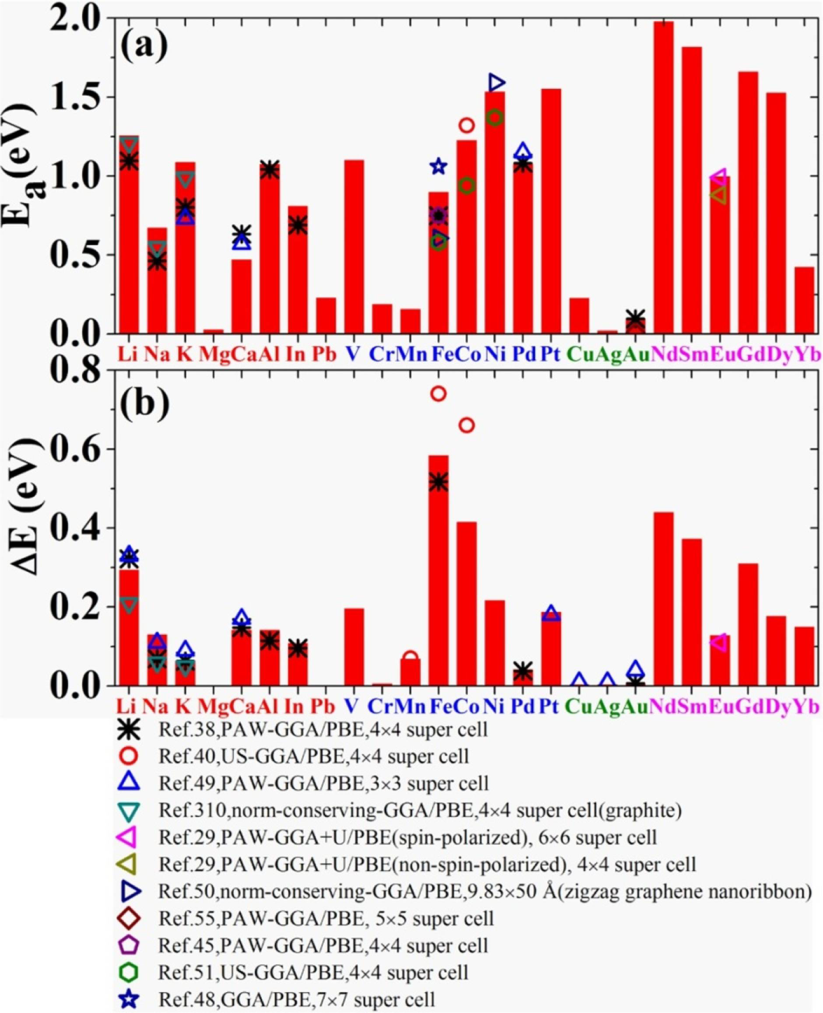
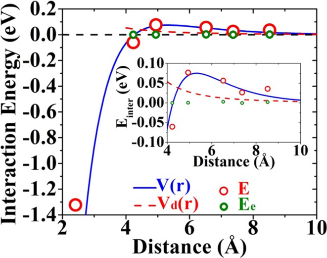
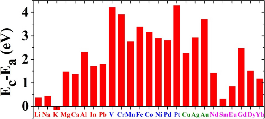
3.1. Energeitcs of Metals on Graphene

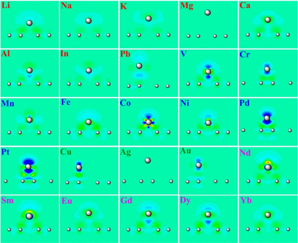
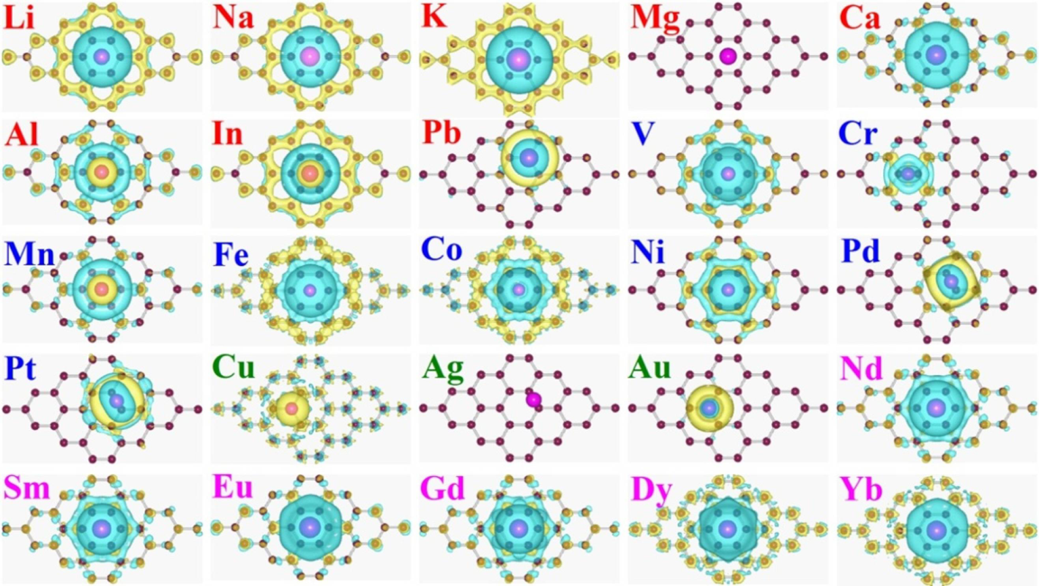
3.2. Interaction Charge Density Distribution

3.3. Microscopy Bonding Nature and Mechanism

4. Properties Induced by Metal Atom Adsorption
4.1. Deformation of Graphene

4.2. Electric Dipole Moment

4.3. Magnetic Moment
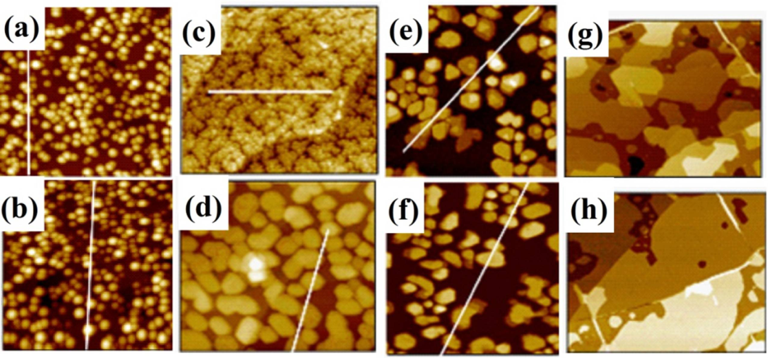
5. Correlation between Growth Morphology and Adatom Adsorption Properties

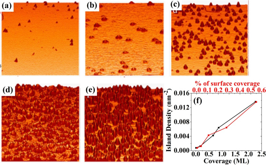
6. Effects of Adatom Interaction on Growth Morphology


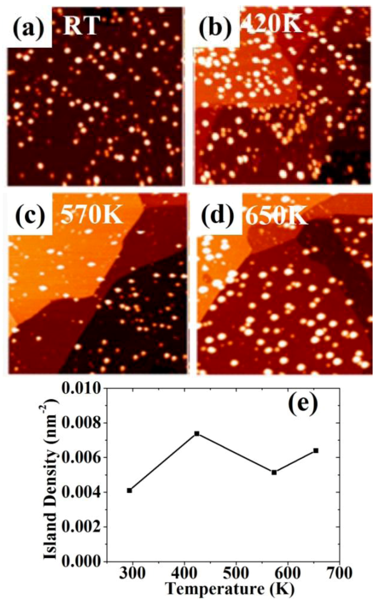
7. Thermal Stability of Metal Nanostructures on Graphene

8. Summary
Acknowledgments
References
- Novoselov, K.S.; Geim, A.K.; Morozov, S.V.; Jiang, D.; Zhang, Y.; Dubonoset, S.V.; Grigorieva, I.V.; Firsov, A.A. Electric field effect in atomically thin carbon films. Science 2004, 306, 666–669. [Google Scholar]
- Novoselov, K.S.; Geim, A.K.; Morozov, S.V.; Jiang, D.; Katsnelson, M.I.; Grigorieva, I.V.; Dubonos, S.V.; Firsov, A.A. Two-dimensional gas of massless Dirac fermions in graphene. Nature 2005, 438, 197–200. [Google Scholar]
- Zhang, Y.; Tan, Y.W.; Stormer, H.L.; Kim, P. Experimental observation of the quantum Hall effect and Berry’s phase in graphene. Nature 2005, 438, 201–204. [Google Scholar] [CrossRef]
- Balandin, A.A.; Ghosh, S.; Bao, W.; Calizo, I.; Teweldebrhan, D.; Miao, F.; Lau, C.N. Superior thermal conductivity of single-layer graphene. Nano Lett. 2008, 8, 902–907. [Google Scholar] [CrossRef]
- Lee, C.; Wei, X.; Kysar, J.W.; Hone, J. Measurement of the elastic properties and intrinsic strength of monolayer graphene. Science 2008, 321, 385–388. [Google Scholar]
- Castro Neto, A.H.; Guinea, F.; Peres, N.M.R.; Novoselov, K.S.; Geim, A.K. The electronic properties of graphene. Rev. Mod. Phys. 2009, 81, 109–162. [Google Scholar] [CrossRef]
- Geim, A.K.; Novoselov, K.S. The rise of graphene. Nat. Mater. 2007, 6, 183–191. [Google Scholar] [CrossRef]
- Das Sarma, S.; Adam, S.; Hwang, E.H.; Rossi, E. Electronic transport in two-dimensional graphene. Rev. Mod. Phys. 2011, 83, 407–470. [Google Scholar] [CrossRef]
- Seneor, P.; Dlubak, B.; Martin, M.B.; Anane, A.; Jaffres, H.; Fert, A. Spintronics with graphene. MRS Bull. 2012, 37, 1245–1254. [Google Scholar] [CrossRef]
- Song, C.L.; Sun, B.; Wang, Y.L.; Jiang, Y.P.; Wang, L.; He, K.; Chen, X.; Zhang, P; Ma, X.C.; Xue, Q.K. Charge-transfer-induced cesium superlattices on graphene. Phys. Rev. Lett. 2012, 108, 156803:1–156803:5. [Google Scholar]
- Virojanadara, C.; Watcharinyanon, S.; Zakharov, A.A.; Johansson, L.I. Epitaxial graphene on 6H-SiC and Li intercalation. Phys. Rev. B 2010, 82, 205402:1–205402:6. [Google Scholar]
- Caragiu, M.; Finberg, S. Alkali metal adsorption on graphite: A review. J. Phys. Condens. Matter 2005, 17, R995–R1024. [Google Scholar] [CrossRef]
- Ferralis, N.; Pussi, K.; Finberg, S.E.; Smerdon, J.; Lindroos, M.; McGrath, R.; Diehl, R.D. Low-energy electron diffraction study of potassium adsorbed on single-crystal graphite and high oriented pyrolytic graphite. Phys. Rev. B 2004, 70, 245407:1–245407:6. [Google Scholar]
- Renard, J.; Lundeberg, M.B.; Folk, J.A.; Pennec, Y. Real-time imaging of K atoms on graphite: Interactions and diffusion. Phys. Rev. Lett. 2011, 106, 156101:1–156101:4. [Google Scholar]
- Knudsen, J.; Feibelman, P.J.; Gerber, T.; Grånäs, E.; Schulte, K.; Stratmann, P.; Andersn, J.N.; Michely, T. Clusters binding to the graphene moiré on Ir(111): X-ray photoemission compared to density functional calculations. Phys. Rev. B 2012, 85, 035407:1–035407:6. [Google Scholar]
- N’Diaye, A.T.; Gerber, T.; Busse, C.; Mysliveček, J.; Coraux, J.; Michely, T. A versatile fabrication method for cluster superlattices. New J. Phys. 2009, 11, 103045:1–103045:19. [Google Scholar]
- Zhou, Z.; Gao, F.; Goodman, D.W. Deposition of metal clusters on single-layer graphene/Ru(0001): Factors that govern cluster growth. Surf. Sci. 2010, 604, L31–L38. [Google Scholar] [CrossRef]
- Park, S.; Shao, Y.; Wan, H.; Rieke, P.C.; Viswanathan, V.V.; Towne, S.A.; Saraf, L.V.; Liu, J.; Lin, Y.; Wang, Y. Design of graphene sheets-supported Pt catalyst layer in PEM fuel cells. Electrochem. Commun. 2011, 13, 258–261. [Google Scholar] [CrossRef]
- Cretu, O.; Rodríguez-Manzo, J.A.; Demortière, A.; Banhart, F. Electron beam-induced formation and displacement of metal clusters on graphene, carbon nanotubes and amorphous carbon. Carbon 2012, 50, 259–264. [Google Scholar] [CrossRef]
- Pi, K.; McCreary, K.M.; Bao, W.; Han, W.; Chiang, Y.F.; Li, Y.; Tsai, S.W.; Lau, C.N.; Kawakami, R.K. Electronic doping scattering by transition metals on graphene. Phys. Rev. B 2009, 80, 075406:1–075406:5. [Google Scholar]
- Zan, R.; Bangert, U.; Ramasse, Q.; Novoselov, K.S. Evolution of gold nanostructures on graphene. Small 2011, 20, 2868–2872. [Google Scholar]
- Xu, Y.; Semidey-Flecha, L.; Liu, L.; Zhou, Z.; Goodman, D.W. Exploring the structure and chemical activity of 2-D gold islands on graphene moiré/Ru(0001). Faraday Discuss. 2011, 152, 267–276. [Google Scholar] [CrossRef]
- Aton, R.; Kreutzer, P. In situ TEM evaluation of the growth kinetics of Au pariticles on highly oriented pyrolithic graphite at elevated temperatures. Phys. Rev. B 2000, 61, 16077–16083. [Google Scholar] [CrossRef]
- Zan, R.; Bangert, U.; Ramasse, Q.; Novoselov, K.S. Metal-graphene interaction studied via atomic resolution scanning transmission electron microscopy. Nano Lett. 2011, 11, 1087–1092. [Google Scholar] [CrossRef]
- Liu, L.; Zhou, Z.; Guo, Q.; Yan, Z.; Yao, Y.; Goodman, D.W. The 2-D growth of gold on single-layer graphene/Ru(0001): Enhancement of CO adsorption. Surf. Sci. 2011, 605, L47–L50. [Google Scholar] [CrossRef]
- Wong, P.K.J.; de Jong, M.P.; Leonardus, L.; Siekman, M.H.; van der Wiel, W.G. Growth mechanism and interface magnetic properties of Co nanostructures on graphite. Phys. Rev. B 2011, 84, 054420:1–054420:5. [Google Scholar]
- Vo-van, C.; Schumacher, S.; Coraux, J.; Sessi, V.; Fruchart, O.; Brookes, N.B.; Ohresser, P.; Michely, T. Magnetism of cobalt nanoclusters on graphene on iridium. Appl. Phys. Lett. 2011, 99, 142504:1–142504:3. [Google Scholar]
- Vo-van, C.; Kassir-Bodon, Z.; Yang, H.; Coraux, J.; Vogel, J.; Pizzini, S.; Bayle-Guillemaud, P.; Chshiev, M.; Ranno Laurent Guisset, V.; David, P.; Salvador, V.; Fruchart, O. Ultrathin epitaxial cobalt films on graphene for spintronic investigations and applications. New J. Phys. 2010, 12, 103040:1–103040:15. [Google Scholar]
- Förster, D.F.; Wehling, T.O.; Schumacher, S.; Rosch, A.; Michely, T. Phase coexistence of clusters and islands: Europium on graphene. New J. Phys. 2012, 14, 023022:1–023022:26. [Google Scholar]
- Sutter, E.; Albrecht, P.; Wang, B.; Bocquet, M.-L.; Wu, L.; Zhu, Y.; Sutter, P. Arrays of Ru nanoclsuters with narrow size distribution template by monolayer graphene on Ru. Surf. Sci. 2011, 605, 1676–1684. [Google Scholar] [CrossRef]
- Rytkönen, K.; Akola, J.; Manninen, M. Density functional study of alkali-metal atoms and monolayers on graphite (0001). Phys. Rev. B 2007, 75, 075401:1–075401:9. [Google Scholar]
- Uthaisar, C.; Barone, V.; Peralta, J.E. Lithium adsorption on zigzag graphene nanoribbons. J. Appl. Phys. 2009, 106, 113715:1–113715:6. [Google Scholar]
- Jin, K.H.; Choi, S.M.; Jhi, S.H. Crossover in the adsorption properties of alkali metals on graphene. Phys. Rev. B 2010, 82, 033414:1–033414:4. [Google Scholar]
- Lugo-Solis, A.; Vasiliev, I. Ab initio study of K adsorption on graphene and carbon nanotubes: Role of long-range ionic force. Phys. Rev. B 2007, 76, 235431:1–235431:8. [Google Scholar]
- Martínez, J.I.; Cabria, I.; López, M.J.; Alonso, J.A. Adsorption of lithium on finite graphitic clusters. J. Phys. Chem. C 2009, 113, 939–941. [Google Scholar]
- Davydov, S.Y. Adsorption of Sodium and cesium on graphite: Work function calculations. Tech. Phys. Lett. 2009, 35, 998–1000. [Google Scholar] [CrossRef]
- Valencia, F.; Romero, A.H.; Ancilotto, F.; Silvestrelli, P.L. Lithium adsorption on graphite from density functional theory calculations. J. Phys. Chem. B 2006, 110, 14832–14841. [Google Scholar]
- Chan, K.T.; Neaton, J.B.; Cohen, M.L. First-principles study of metal adatom adsorption on graphene. Phys. Rev. B 2008, 77, 235430:1–235430:12. [Google Scholar]
- Sanchez-Paisal, Y.; Sanchez-Portal, D.; Ayuela, A. Ab initio calculations of zirconium adsorption and diffusion on graphene. Phys. Rev. B 2009, 80, 045428:1–045428:10. [Google Scholar]
- Mao, Y.; Yuan, J.; Zhong, J. Density functional calculation of transition metal adatom adsorption on graphene. J. Phys. Condens. Matter 2008, 20. [Google Scholar] [CrossRef]
- Sevinçli, H.; Topsakal, M.; Durgun, E.; Ciraci, S. Electronic and magnetic properties of 3d transition metal atom adsorbed graphene and graphene nanoribbons. Phys. Rev. B 2008, 77, 195434:1–195434:7. [Google Scholar]
- Zanella, I.; Fagan, S.B.; Mota, R.; Fazzio, A. Electric and magnetic properties of Ti and Fe on graphene. J. Phys. Chem. C 2008, 112, 9163–9168. [Google Scholar] [CrossRef]
- Zólyomi, V.; Rusznyák, Á.; Kürti, J.; Lambert, C.J. First principles study of the binding of 4d and 5d transition metals to graphene. J. Phys. Chem. C 2010, 114, 18548–18552. [Google Scholar] [CrossRef]
- Wehling, T.O.; Balatsky, A.V.; Katsnelson, M.I.; Lichtenstein, A.I.; Rosch, A. Orbitally controlled Kondo effect of Co adatoms on grapheme. Phys. Rev. B 2010, 81, 115427:1–115427:6. [Google Scholar]
- Porter, C.D.; Stroud, D. Clustering and magnetic anisotropy of Fe adatoms on graphene. Phys. Rev. B 2012, 85, 235452:1–235452:10. [Google Scholar]
- Nemec, N.; Tománek, D.; Cuniberti, G. Contact dependence of carrier injection in carbon nanotubes: An ab initio study. Phys. Rev. Lett. 2006, 96, 076802:1–076802:4. [Google Scholar]
- Krasheninnikov, A.V.; Lehtinen, P.O.; Foster, A.S.; Pyykkö, P.; Nieminen, R.M. Embedding transition-metal atoms in graphene: Structure, bonding, and magnetism. Phys. Rev. Lett. 2009, 102, 126807:1–126807:4. [Google Scholar]
- Cao, C.; Wu, M.; Jiang, J.; Cheng, H.P. Transition metal adatom and dimer adsorbed on graphene: Induced magnetization and electronic structures. Phys. Rev. B 2010, 81, 205424:1–205424:9. [Google Scholar]
- Ishii, A.; Yamamoto, M.; Asano, H.; Fujiwara, K. DFT calculation for adatom adsorption on graphene sheet as a prototype of carbon nano tube functionalization. J. Phys. Conf. Ser. 2008, 100, 052087:1–052087:4. [Google Scholar]
- Longo, R.C.; Carrete, J.; Ferrer, J.; Gallego, L.J. Structural, magnetic, and electronic properties of Nin and Fen nanostructures (n = 1-4) adsorbed on zigzag nanoribbons. Phys. Rev. B 2010, 81, 115418:1–115418:10. [Google Scholar]
- Johll, H.; Kang, H.C. Density functional theory of Fe, Co, and Ni adatoms and dimmers adsorbed on graphene. Phys. Rev. B 2009, 79, 245416:1–245416:18. [Google Scholar]
- Duffy, D.M.; Blackman, J.A. Magnetism of 3d transition-metal adatoms and dimmers on graphite. Phys. Rev. B 1998, 58, 7443–7449. [Google Scholar] [CrossRef]
- Wu, M.; Liu, E.Z.; Ge, M.Y.; Jiang, J.Z. Stability, electronic, and magnetic behaviors of Cu adsorbed graphene: A first-principles study. Appl. Phys. Lett. 2009, 94, 102505:1–102505:3. [Google Scholar]
- Aktürk, O.Ü.; Tomak, M. AunPtn clusters adsorbed on graphene studied by first-principles calculations. Phys. Rev. B 2009, 80, 085417:1–085417:6. [Google Scholar]
- Amft, M.; Sanyal, B.; Eriksson, O.; Skorodumova, N.V. Small gold clusters on graphene, their mobility and clustering: A DFT study. J. Phys. Condens. Matter 2011, 23. [Google Scholar] [CrossRef]
- Varns, R.; Strange, P. Stability of gold atoms and dimers adsorbed on graphene. J. Phys. Condens. Matter 2008, 20, 225005:1–225005:8. [Google Scholar]
- Okazaki-Maeda, K.; Morikawa, Y.; Tanaka, S.; Kohyama, M. Structures of Pt clusters on graphene by first-principles calculations. Surf. Sci. 2010, 604, 144–154. [Google Scholar] [CrossRef]
- Zhou, Y.G.; Zu, X.T.; Gao, F.; Lv, H.F.; Xiao, H.Y. Adsorption-induced magnetic properties and metallic behavior of graphene. Appl. Phys. Lett. 2009, 95, 123119:1–123119:3. [Google Scholar]
- Balog, R.; Jørgensen, B.; Wells, J.; Lægsgaard, E.; Hofmann, P.; Besenhacher, F.; Hornekær, L. Atomic hydrogen adsorbate structures on graphene. J. Am. Chem. Soc. 2009, 131, 8744–8745. [Google Scholar]
- Li, W.; Zhao, M.; Xia, Y.; Zhang, R.; Mu, Y. Covalent-adsorption induced magnetism in graphene. J. Mater. Chem. 2009, 19, 9274–9282. [Google Scholar] [CrossRef]
- Ivanovskaya, V.V.; Zobelli, A.; Teillet-Billy, D.; Rougeau, N.; Sidis, V.; Briddon, P.R. Hydrogen adsorption on graphene: A first principles study. Eur. Phys. J. B 2010, 76, 481–486. [Google Scholar] [CrossRef]
- Wehling, T.O.; Katsnelson, M.I.; Lichtenstein, A.I. Impurities on graphene: Midgap states and migration barriers. Phys. Rev. B 2009, 80, 085428:1–085428:7. [Google Scholar]
- Wang, W.X.; liang, S.H.; Yu, T.; Li, D.H.; Li, Y.B.; Han, X.F. The study of interaction between graphene and metals by Raman spectroscopy. J. Appl. Phys. 2011, 109, 07C501:1–07C501:3. [Google Scholar]
- Khomyakov, P.A.; Giovannetti, G.; Rusu, P.C.; Brocks, G.; van den Brink, J.; Kelly, P.J. First-principles study of the interaction and charge transfer between graphene and metals. Phys. Rev. B 2009, 79, 195425:1–195425:12. [Google Scholar]
- Yoo, E.J.; Okata, T.; Akita, T.; Kohyama, M.; Nakamura, J.; Honma, I. Enhanced electrocatalytic activity of Pt subnanoclusters on graphene nanosheet surface. Nano Lett. 2009, 9, 2255–2259. [Google Scholar]
- Kou, R.; Shao, Y.; Wang, D.; Engelhard, M.H.; Kwak, J.H.; Wang, J.; Viswanathan, V.V.; Wang, C.; Lin, Y.; Wang, Y.; Aksay, I.A.; Liu, J. Enhanced activity and stability of Pt catalysts on functionalized graphene sheets for electrocatalytic oxygen reduction. Elctrochem. Commun. 2009, 11, 954–957. [Google Scholar] [CrossRef]
- Seger, B.; Kamat, P.V. Electrocatalytically active graphene-platinum naocomposites. Role of 2-D carbon support in PEM fuel cell. J. Phys. Chem. C 2009, 113, 7990–7995. [Google Scholar] [CrossRef]
- Seo, M.H.; Choi, S.M.; Kim, H.J.; Kim, W.B. The graphene-supported Pd and Pt catalysts for highly active oxygen reduction reaction in an alkaline condition. Electrochem. Commun. 2011, 13, 182–185. [Google Scholar] [CrossRef]
- Bong, S.; Kim, Y.R.; Kim, I.; Wooa, S.; Uhmb, S.; Lee, J.; Kim, H. Graphene supported electrocatalysts for methanol oxidation. Electrochem. Commun. 2010, 12, 129–131. [Google Scholar] [CrossRef]
- Dong, L.; Gari, R.R.S.; Li, Z.; Graig, M.M.; Hou, S. Graphene-supported platinum-ruthenium nanoparticles with high electrocatalytic activity for methanol ethanol oxidation. Carbon 2010, 48, 781–787. [Google Scholar] [CrossRef]
- Liu, X.; Wang, C.Z.; Yao, Y.X.; Lu, W.C.; Hupalo, M.; Tringides, M.C.; Ho, K.M. Bonding and charge transfer by metal adatom adsorption on graphene. Phys. Rev. B 2011, 83, 235411:1–235411:12. [Google Scholar]
- Liu, X.; Wang, C.Z.; Hupalo, M.; Yao, Y.X.; Tringides, M.C.; Lu, W.C.; Ho, K.M. Adsorption and growth morphology of rare earth metals on graphene studied by ab initio calculations and scanning tunneling microscopy. Phys. Rev. B 2010, 82, 245408:1–245408:7. [Google Scholar]
- Hupalo, M.; Liu, X.; Wang, C.Z.; Lu, W.C.; Yao, Y.X.; Ho, K.M.; Tringides, M.C. Metal nanostructure formation on graphene: Weak versus strong bonding. Adv. Mater. 2011, 23, 2082–2087. [Google Scholar] [CrossRef]
- Hupalo, M.; Binz, S.; Tringides, M.C. Strong metal adatom substrate interaction of Gd and Fe with graphene. J. Phys. Condens. Matter 2011, 23, 045005:1–045005:7. [Google Scholar]
- Liu, X.; Wang, C.Z.; Hupalo, M.; Lu, W.C.; Thiel, P.A.; Ho, K.M.; Tringides, M.C. Fe-Fe adatom interaction and growth morphology on graphene. Phys. Rev. B 2011, 84, 235446:1–235446:5. [Google Scholar]
- Liu, X.; Wang, C.Z.; Hupalo, M.; Lu, W.C.; Tringides, M.C.; Yao, Y.X.; Ho, K.M. Metals on graphene: Correlation between adatom adsorption behavior and growth morphology. Phys. Chem. Chem. Phys. 2012, 14, 9157–9166. [Google Scholar] [CrossRef]
- Binz, S.M.; Hupalo, M.; Liu, X.; Wang, C.Z.; Lu, W.C.; Thiel, P.A.; Ho, K.M.; Conrad, E.H.; Tringides, M.C. High Island Densities and Long Range Repulsive Interactions: Fe on Epitaxial Graphene. Phys. Rev. Lett. 2012, 109, 026103:1–026103:5. [Google Scholar]
- Liu, X.; Hupalo, M.; Wang, C.Z.; Lu, W.C.; Thiel, P.A.; Ho, K.M.; Tringides, M.C. Growth morphology and thermal stability of metal islands on graphene. Phys. Rev. B 2012, 86, 081414:1–081414:5. [Google Scholar]
- Coraux, J.; N’Diaye, A.T.; Engler, M.; Busse, C.; Wall, D.; Buckanie, N.; Heringdorf, F.-J.M.; Gastel, R.; Poelsema, B.; Michely, T. Growth of graphene on Ir(111). New J. Phys. 2009, 11, 023006:1–023006:22. [Google Scholar]
- Coraux, J.; N'Diaye, A.T.; Busse, C.; Michely, T. Structural coherency of graphene on Ir(111). Nano Lett. 2008, 8, 565–570. [Google Scholar] [CrossRef]
- N’Diaye, A.T.; Coraux, J.; Plasa, T.N.; Busse, C.; Michely, T. Structure of epitaxial graphene on Ir(111). New J. Phys. 2008, 10, 043033:1–043033:16. [Google Scholar]
- Bartelt, N.C.; McCarty, K.F. Graphene growth on metal surface. MRS Bull. 2012, 37, 1158–1165. [Google Scholar] [CrossRef]
- Wintterlin, J.; Bocquet, M.-L. Graphene on metal surfaces. Surf. Sci. 2009, 603, 1841–1852. [Google Scholar] [CrossRef]
- Giovannetti, G.; Khomyakov, P.A.; Brocks, G.; Karpan, V.M.; van den Brink, J.; Kelly, P.J. Doping graphene with metal contacts. Phys. Rev. Lett. 2008, 101, 026803:1–026803:4. [Google Scholar]
- Dedkov, Y.S.; Fonin, M.; Rüdiger, U.; Laubschat, C. Rashba effect in the graphene/Ni(111) system. Phys. Rev. Lett. 2008, 100, 107602:1–107602:4. [Google Scholar]
- Nie, S.; Wofford, J.M.; Bartelt, N.C.; Dubon, O.D.; McCarty, K.F. Origin of the mosaicity in graphene grown on Cu(111). Phys. Rev. B 2011, 84, 155425:1–155425:7. [Google Scholar]
- Varykhalov, A.; Sánchez-Barriga, J.; Shikin, A.M.; Biswas, C.; Vescovo, E.; Rybkin, A.; Marchenko, D.; Rader, O. Electronic and magnetic properties of quasifreestanding graphene on Ni. Phys. Rev. Lett. 2008, 101, 157601:1–157601:4. [Google Scholar]
- Wofford, J.M.; Starodub, E.; Walter, A.L.; Nie, S.; Bostwick, A.; Bartelt, N.C.; Thürmer, K.; Rotenberg, E.; McCarty, K.F.; Dubon, O.D. Extraordinary epitaxial alignment of graphene islands on Au(111). New J. Phys. 2012, 14, 053008:1–053008:10. [Google Scholar]
- Vázquez de Parga, A.L.; Calleja, F.; Borca, B.; Passeggi, M.C.G., Jr.; Hinarejos, J.J.; Guinea, F.; Miranda, R. Periodically rippled graphene: Growth and spatially resolved electronic structure. Phys. Rev. Lett. 2008, 100, 056807:1–056807:4. [Google Scholar]
- Wong, S.L.; Huang, H.; Chen, W.; Wee, A.T.S. STM studies of epitaxial graphene. MRS Bull. 2012, 37, 1195–1202. [Google Scholar] [CrossRef]
- Hupalo, M.; Conrad, E.H.; Tringides, M.C. Growth mechanism for epitaxial graphene on vicinal 6H-SiC(0001) surface: A scanning tunneling microscopy study. Phys. Rev. B 2009, 80, 041401:1–041401:4. [Google Scholar]
- Lu, W.; Boeckl, J.J.; Mitchel, W.C. A critical review of growth of low-dimensional carbon nanostructures on SiC(0001): Impact of growth environment. J. Phys. D 2010, 43. [Google Scholar] [CrossRef]
- Al-Temimy, A.; Riedl, C.; Starke, U. Low temperature growth of epitaxial graphene on SiC induced by carbon evaporation. Appl. Phys. Lett. 2009, 95, 231907:1–231907:3. [Google Scholar]
- Park, J.H.; Mitchel, W.C.; Grazulis, L.; Eyink, K.; Smith, H.E.; Hoelscher, J.E. Role of extended defected SiC interface layer on the growth of epitaxial graphene on SiC. Carbon 2011, 49, 631–635. [Google Scholar]
- Hass, J.; de Heer, W.A.; Conrad, E.H. The growth and morphology of epitaxial multilayer graphene. J. Phys. Condens. Matter 2008, 20. [Google Scholar] [CrossRef]
- Gierz, I.; Riedl, C.; Starke, U.; Ast, C.R.; Kern, K. Atomic hole doping of graphene. Nano Lett. 2008, 8, 4603–4607. [Google Scholar] [CrossRef]
- McChesney, J.L.; Bostwick, A.; Ohta, T.; Seyller, T.; Horn, K.; González, J.; Rotenberg, E. Extended van hove singularity and superconducting instability in doped graphene. Phys. Rev. Lett. 2010, 104, 136803:1–136803:4. [Google Scholar]
- Gierz, I.; Suzuki, T.; Weitz, R.T.; Lee, D.S.; Krauss, B.; Riedl, C.; Starke, U.; Höchst, H.; Smet, J.H.; Ast, C.R.; Kern, K. Electronic decoupling of an epitaxial graphene monolayer by gold intercalation. Phys. Rev. B 2010, 81, 235408:1–235408:6. [Google Scholar]
- Sandin, A.; Jayasekera, T.; Rowe, J.E.; Kim, K.W.; Nardelli, M.B.; Dougherty, D.B. Multiple coexisting intercalation structures of sodium in epitaxial graphene-SiC interfaces. Phys. Rev. B 2012, 85, 125410:1–125410:5. [Google Scholar]
- Evans, J.W.; Thiel, P.A.; Bartelt, M.C. Morphological evolution during epitaxial thin film growth: Formation of 2D islands and 3D mounds. Surf. Sci. Rep. 2006, 61, 1–128. [Google Scholar]
- Venables, J.A.; Spiller, G.D.T.; Hanbucken, M. Nucleation and growth of thin films. Rep. Prog. Phys. 1984, 47, 399–459. [Google Scholar] [CrossRef]
- Stroscio, J.A.; Pierce, D.T.; Dragoset, R.A. Homoepitaxial growth of iron and a real space view of reflection-high-energy-electron diffraction. Phys. Rev. Lett. 1993, 70, 3615–3618. [Google Scholar] [CrossRef]
- Hupalo, M.; Tringides, M.C. Ultrafast kinetics in Pb/Si(111) from the collective spreading of the wetting layer. Phys. Rev. B 2007, 75, 235443:1–235443:7. [Google Scholar]
- Chan, T.L.; Yao, Y.X.; Wang, C.Z.; Lu, W.C.; Li, J.; Qian, X.F.; Yip, S.; Ho, K.M. Highly localized quasiatomic minimal basis orbitals for Mo from ab initio calculations. Phys. Rev. B 2007, 76, 205119:1–205119:10. [Google Scholar]
- Qian, X.F.; Li, J.; Qi, L.; Wang, C.Z.; Chan, T.L.; Yao, Y.X.; Ho, K.M.; Yip, S. Quasiatomic orbitals for ab initio tight-binding analysis. Phys. Rev. B 2008, 78, 245112:1–245112:22. [Google Scholar]
- Yao, Y.X.; Wang, C.Z.; Ho, K.M. Chemical bonding analysis for solid-state systems using intrinsic oriented quasiatomic minimal-basis-set orbitals. Phys. Rev. B 2010, 81, 235119:1–235119:6. [Google Scholar]
- Mayer, I. Charge, bond order and valence in the ab initio SCF theory. Chem. Phys. Lett. 1983, 97, 270–274. [Google Scholar] [CrossRef]
- Shytov, A.V.; Abanin, D.A.; Levitov, L.S. Long-Range interaction between adatoms in graphene. Phys. Rev. Lett. 2009, 103, 016806:1–016806:4. [Google Scholar]
- Bena, C. Effect of a single localized impurity on the local density of sates in monolayer and bilyaer graphene. Phys. Rev. Lett. 2008, 100, 076601:1–076601:4. [Google Scholar]
- Bacsi, A.; Virosztek, A. Local density of states and Friedel oscillations in graphene. Phys. Rev. B 2010, 82, 193405:1–193405:4. [Google Scholar]
- Cheianov, V.V.; Syljuåsen, O.; Altshuler, B.L.; Falko, V.I. Ordered states of adatoms on graphene. Phys. Rev. B 2009, 80, 233409:1–233409:4. [Google Scholar]
- Saremi, S. RKKY in half-filled bipartite lattices: Graphene as an example. Phys. Rev. B 2007, 76, 184430:1–184430:6. [Google Scholar]
- Cheianov, V.V.; Falko, V.I. Friedel oscillations, impurity scattering, and temperature dependence of resistivity in graphene. Phys. Rev. Lett. 2006, 97, 226801:1–226801:4. [Google Scholar]
© 2013 by the authors; licensee MDPI, Basel, Switzerland. This article is an open access article distributed under the terms and conditions of the Creative Commons Attribution license (http://creativecommons.org/licenses/by/3.0/).
Share and Cite
Liu, X.; Wang, C.-Z.; Hupalo, M.; Lin, H.-Q.; Ho, K.-M.; Tringides, M.C. Metals on Graphene: Interactions, Growth Morphology, and Thermal Stability. Crystals 2013, 3, 79-111. https://doi.org/10.3390/cryst3010079
Liu X, Wang C-Z, Hupalo M, Lin H-Q, Ho K-M, Tringides MC. Metals on Graphene: Interactions, Growth Morphology, and Thermal Stability. Crystals. 2013; 3(1):79-111. https://doi.org/10.3390/cryst3010079
Chicago/Turabian StyleLiu, Xiaojie, Cai-Zhuang Wang, Myron Hupalo, Hai-Qing Lin, Kai-Ming Ho, and Michael C. Tringides. 2013. "Metals on Graphene: Interactions, Growth Morphology, and Thermal Stability" Crystals 3, no. 1: 79-111. https://doi.org/10.3390/cryst3010079
APA StyleLiu, X., Wang, C.-Z., Hupalo, M., Lin, H.-Q., Ho, K.-M., & Tringides, M. C. (2013). Metals on Graphene: Interactions, Growth Morphology, and Thermal Stability. Crystals, 3(1), 79-111. https://doi.org/10.3390/cryst3010079