Article

Effects of Strain on Notched Zigzag Graphene Nanoribbons

Department of Physics, The University of York, Heslington, York, YO10 5DD, UK
*
Author to whom correspondence should be addressed.
Crystals 2013, 3(1), 38-48; https://doi.org/10.3390/cryst3010038
Submission received: 19 November 2012 / Revised: 28 December 2012 / Accepted: 9 January 2013 / Published: 23 January 2013
(This article belongs to the Special Issue Graphenes)

Abstract

:
The combined effects of an asymmetric (square or V-shaped) notch and uniaxial strain are studied in a zigzag graphene nanoribbon (ZGNR) device using a generalized tight-binding model. The spin-polarization and conductance-gap properties, calculated within the Landauer–Büttiker formalism, were found to be tunable for uniaxial strain along the ribbon-length and ribbon-width for an ideal ZGNR and square (V-shaped) notched ZGNR systems. Uniaxial strain along the ribbon-width for strains ≥10% initiated significant notch-dependent reductions to the conduction-gap. For the V-shaped notch, such strains also induced spin-dependent changes that result, at 20% strain, in a semi-conductive state and metallic state for each respective spin-type, thus demonstrating possible quantum mechanisms for spin-filtration.

1. Introduction

The structure and chemical functionalization of the edges of graphene nanoribbons (GNRs) have a pronounced effect on their properties, such as the band gap and electronic transport [1,2,3,4,5,6,7,8,9,10,11,12]. One example of patterning in GNRs that has recently been studied is a notch [8,9,13,14,15,16]. Notches made on one edge of a GNR (i.e., an asymmetric notch) have been shown, in theory, to break the spin-symmetry in zigzag graphene nanoribbons (ZGNRs) and to give rise to spin-dependent transport [8,9,13,14]. Such effects may prove to be of interest for spintronics [8], with this form of patterning also being within the realm of top-down patterning approaches [15,16,17].
In addition to patterning, uniaxial strain has also been used to control the properties of GNR and bulk graphene devices [18,19,20,21,22,23,24,25,26,27,28,29,30]. Strain can intrinsically arise due to lattice mismatch between the graphene device and the substrate onto which it is deposited [31,32,33], or can be directly applied (e.g., the application of uniaxial tensile strain on suspended graphene samples) [34,35]. Strain has also been used to perturb the band gap [18,19,20,21,22,23,24] and transport properties [20,28] in a controllable fashion, with theoretical and experimental evidence suggesting that strain can lead to metal–semiconductor transitions in bulk graphene and nanographene [20,21].
In this work, the combined effects of an asymmetric notch and uniaxial strain on the magnetism and coherent transport properties of ZGNR devices (Figure 1) will be explored. Such systems have been previously studied using a simple (i.e., non-interacting) tight-binding (TB) model [28]. Here, we will study these effects within the context of a generalized TB model that takes into account up to third nearest-neighbor hopping and contains a mean-field Hubbard-U interaction term [13], thereby enabling the study of the spin-dependent properties of these systems. We will investigate the tunability, as well as the potential for spin-dependent transport and spin-filtering. Given that graphene can be stretched up to 12% elastically, and up to 20% [34,36] before failure, these results may be of interest for examining the potential of patterned graphene nanosystems within the context of “flexible electronics” [37,38,39].
Figure 1. An unstrained ZGNR device (ribbon dimensions ∼40.6 nm × 13.5 nm) with an asymmetric (a) square notch (∼14.8 nm × 8.53 nm); and (b) V-shaped notch (∼8.53 nm depth, with lengths ∼14.8 nm at the widest, and ∼4.9 nm at the narrowest).
Crystals 03 00038 g001

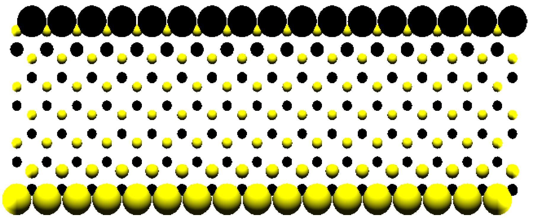
2. Theoretical Method

A generalized tight-binding (TB) model with a Hubbard-U (on-site) Coulomb interaction term was used to model the ZGNRs [13],
Crystals 03 00038 i002
Here, Crystals 03 00038 i003 
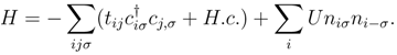
is the Fermion creation(destruction) operator, which creates(destroys) an electron with spin σ = {↑, ↓} at site i(j), and n= 1 or 0 is the spin-dependent number operator, where ni−σ refers to the number operator corresponding to the opposite spin, −σ. The hopping term tij is taken up to third-nearest-neighbor and corresponds to the energy required for a spin to hop between sites i and j. H.c. refers to the Hermitian conjugate. The parameter U denotes the strength of the local Coulomb interaction energy between opposite spins—the so-called Hubbard-U [40]—which has been linearized using the mean-field approximation
Crystals 03 00038 i004
where 〈n〉 denotes the local spin-occupancy taken within the quantum average [13,41]. Thus, Equation (1) can be decoupled into two spin-dependent Hamiltonians, which are then solved self-consistently [41]. The local spin-polarization (pi) is determined from the local spin-occupancies, such that
Crystals 03 00038 i005
The coherent transport properties of the ZGNRs have been calculated using the generalized TB model (Equations (1) and (2)) applied within the Landauer-Bü ttiker formalism [42], and assuming that the device has semi-infinite, ideal ZGNR leads. The spin-dependent conductance Gσ (E) at energy E is obtained from the transmission function Tσ (E), such that
Crystals 03 00038 i006
where e and h are the electron charge and Planck’s constant, respectively, and
Crystals 03 00038 i007
where Crystals 03 00038 i008 
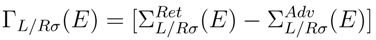
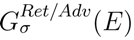
are the retarded/advanced Green’s functions. The ΓL/Rσ (E) matrices are calculated from
Crystals 03 00038 i009
Where
Crystals 03 00038 i010
are the retarded/advanced self-energies. Here, VL/R denotes the coupling between the GNR device and the Left(L)/Right(R) lead, and Crystals 03 00038 i011 
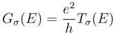
(E) are the retarded/advanced surface Green’s functions for the leads, which have been obtained using the decimation iteration method [43].
The parameters for the generalized TB model (Equation (1)) have been obtained by fitting to local spin-density approximation (LSDA), density functional theory (DFT) results for hydrogen-passivated GNRs, such that U = 2.0, and tij corresponds to t1 = 2.7, t2 = 0.20, and t3 = 0.18, for first, second and third nearest-neighbor hopping, respectively (in units of eV) [13]. Used within the coherent transport formalism, this model faithfully reproduces ab initio transport results [13,14] calculated using TranSIESTA [44], which applies a non-equilibrium Green’s function formalism to the SIESTA DFT method [45,46].
Uniaxial strain has been added to the device and the leads by perturbing the generalized TB model via Harrison scaling [22,27,28,47], such that
Crystals 03 00038 i012
where tij and Crystals 03 00038 i013 
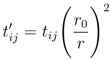
are the unstrained and strained hopping parameters connecting sites i and j, and r0 and r are the unstrained and strained bond lengths respectively. The strain is calculated using
Crystals 03 00038 i014
with uniaxial strain in the x-direction (x) defined along the ribbon-length and uniaxial strain in the y-direction (y) defined along the ribbon-width. A Poisson ratio, P = 0.186, obtained from the DFT calculations of Liu et al. [33] is also used, such that
Crystals 03 00038 i015

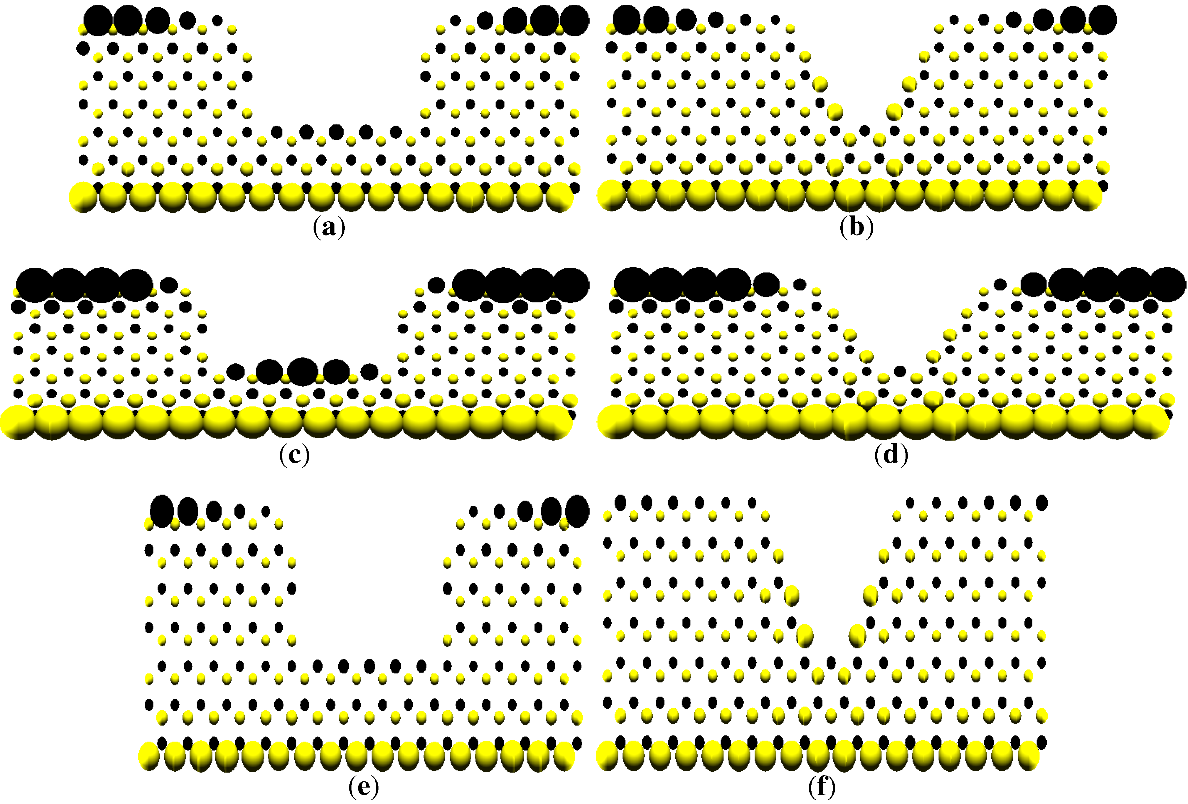
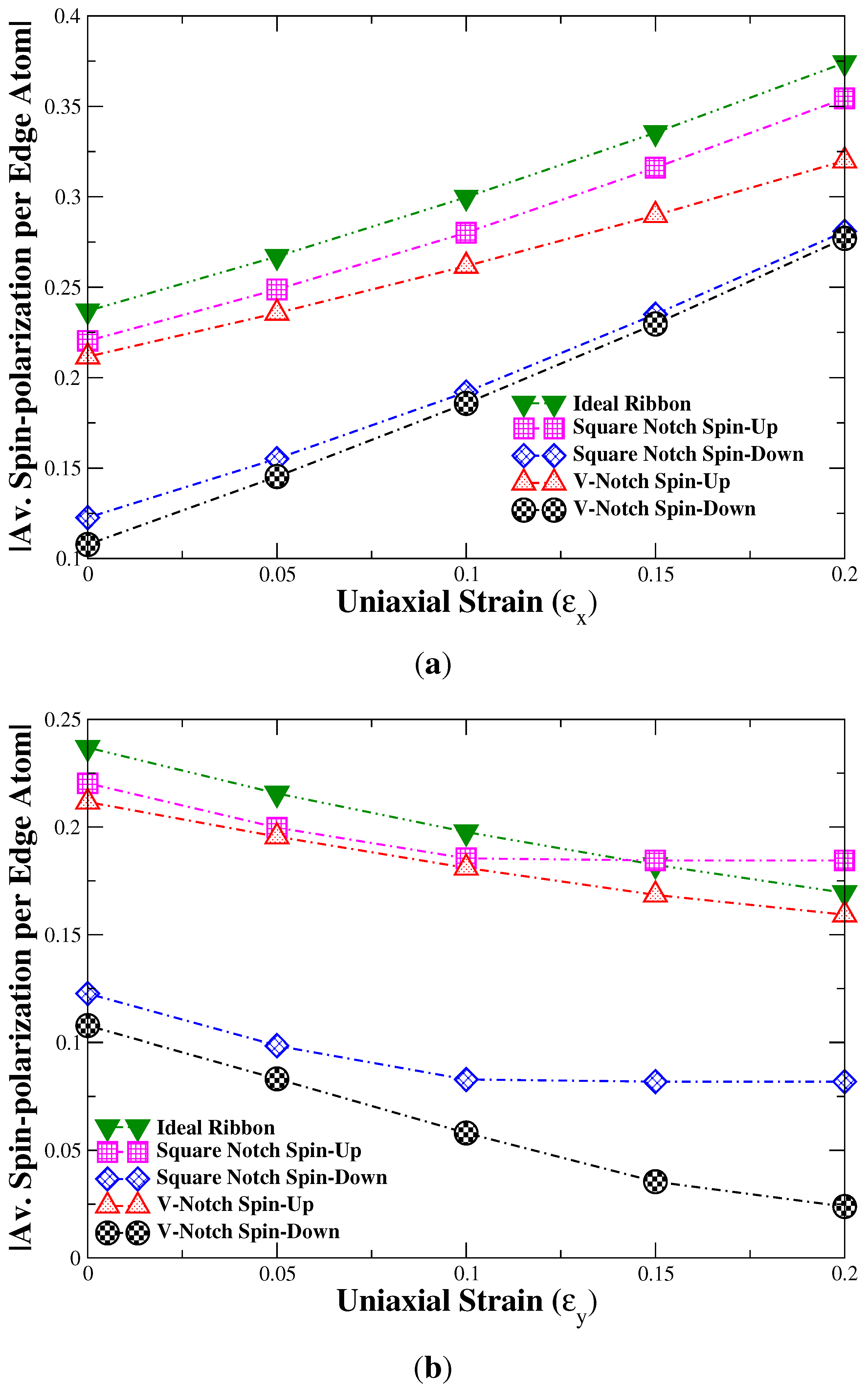
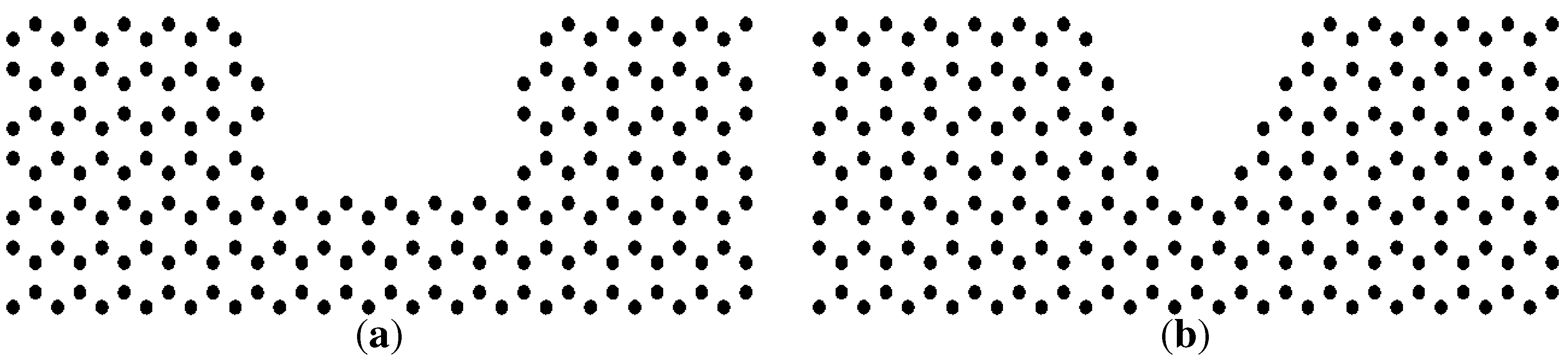
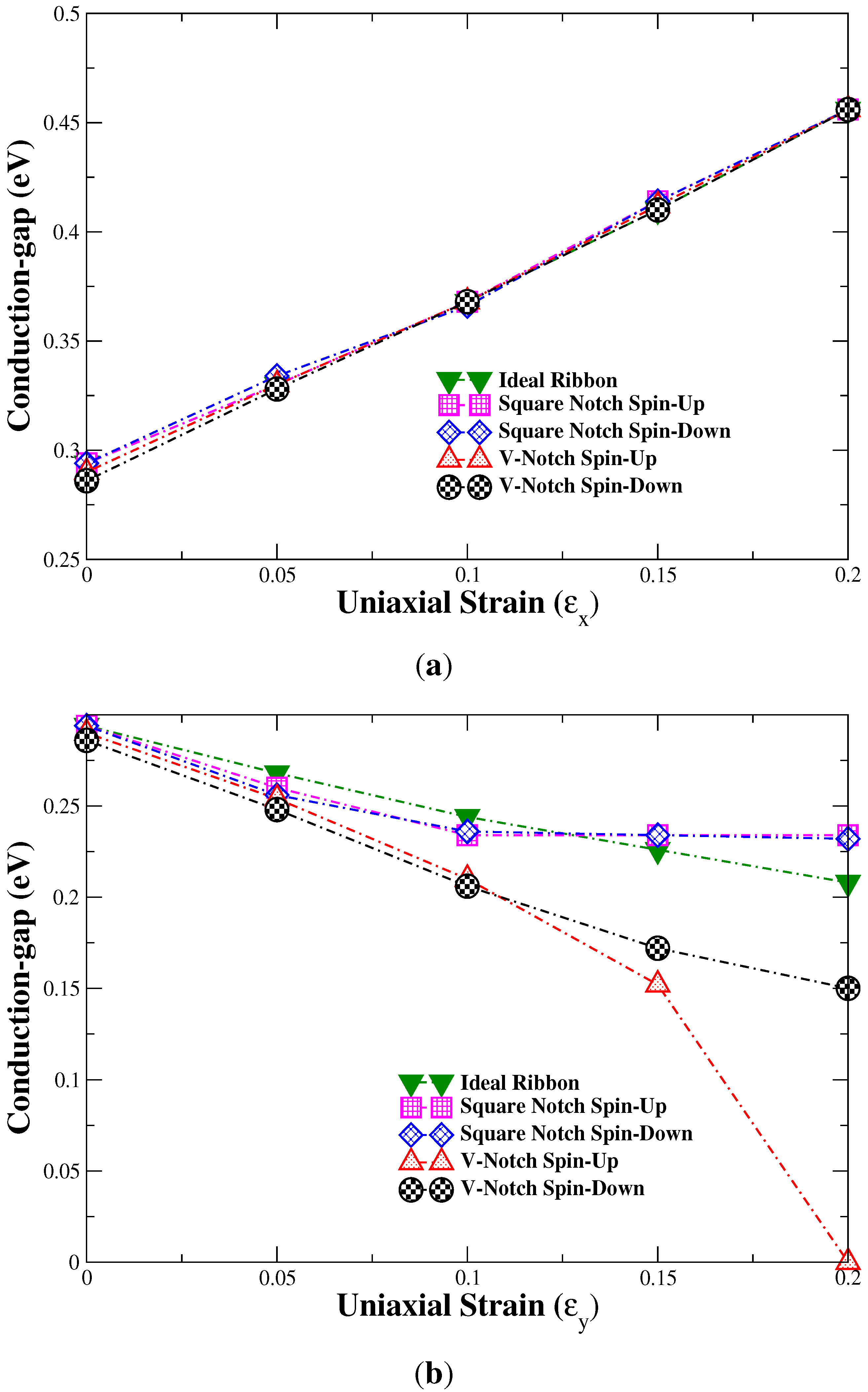
3. Results and Discussion

The calculated local spin-polarization (Equation 3) for an ideal ZGNR (Figure 2) demonstrates the known theoretical prediction of an anti-ferromagnetic spin-structure (symmetric across the edges of the ribbon) with a zero net spin-polarization [48]. The introduction of a square, or V-shaped, notch into this system breaks the spin-symmetry, which is shown in the unstrained local spin-polarization results for the square notch and V-shaped notched ZGNRs, respectively (Figure 3a,b).
Figure 2. (Color on-line). Pictorial representation of the local spin-polarization for an ideal ZGNR device (unstrained). Yellow (black) corresponds to a net spin-up (down). The magnitude of the spin-polarization (Equation 3) is indicated by the circle radius.
Crystals 03 00038 g002
For the notched ZGNRs, a maximum strain of 20% in the x-direction is found to increase the local spin-polarization, particularly across the edges of the device (Figure 3c,d). This increase in the local spin-polarization can be understood from the lengthening of the x-component of the bonds, which results in a net reduction in the spin-itinerancy, and thus increased Hubbard-U effects in the device region. In notched ZGNRs that have a maximum 20% strain in the y-direction, however, the converse is true. The compression in the x-direction, which occurs from the strain in the y, increases the spin-itinerancy along the direction of the ribbon-length, therefore decreasing the local spin-polarization seen in both the square and V-shaped notch systems (Figure 3e,f). The reduced spin-polarization, in general, arises from a greater relative change in local occupancy for spin-up between the y-strained and unstrained notch systems. For the V-shaped notch, this relative change in spin-up occupancy between the strained and the unstrained systems was found to be three times greater than that for spin-down. Thus, the decrease in local spin-polarization for the V-shaped notch is attributed to an increased itinerancy with respect to spin-up. The decrease in the local spin-polarization is particularly apparent across the top and bottom edges of the device, however, results in a trapping of spin on the edge-atoms at the bottom of the V-notch region (Figure 3f).
Figure 3. (Color on-line). Local spin-polarization for a zero-strained ZGNR device with a (a) square notch, and (b) V-shaped notch. 20% (maximum) x-strained (c) square, and (d) V- shaped notched ZGNRs, and 20% (maximum) y-strained (e) square notch, and (f) V-shaped notched ZGNRs. Yellow (black) refers to spin-up (down), with the magnitude of the spin- polarization (Equation 3) being indicated by the circle radius. N.b., the local spin-polarization on the atoms that are directly coupled to the leads, is equal to that of an ideal (unstrained or strained) ZGNR.
Crystals 03 00038 g003
The average spin-polarization per edge-atom (including the notch region) in the ideal and notched systems for increasing uniaxial strain is shown in Figure 4. For uniaxial strain in the x-direction (Figure 4a), an increase in the average spin-polarization per edge-atom occurs for both spin-types as a function of the increasing strain, with similar trends seen in all systems. These trends support the local spin-occupancy results at 20% x-strain (Figure 3c,d), which showed an increase in the local spin-polarization, particularly across the edges of the device. For uniaxial strain in the y-direction (Figure 4b), the average spin-polarization per edge-atom in the notched devices decreases as a function of increasing strain, then starts to level off at high values of strain (> 10%). This leveling off of the average spin-polarization per edge-atom is not apparent for the V-shaped notch system due to the strain in the y-direction, which works to physically close the notch, and hence continues to improve the overall itinerancy in the device.
Figure 4. (Color on-line). The effects of uniaxial strain m the (a) x-direction, and (b) y-direction on the average spin-polarization (net spin-up & net spin-down) per edge-atom (including the notch region) for an ideal, square notch and V-shaped notch ZGNR system. The results for the ideal ribbon show similar trends to those reported in [23].
Crystals 03 00038 g004
The dependence of the device properties on strain can also be seen in the conductance-gap trends for these systems. We define the conductance-gap as the zero-conductance region around the Fermi energy, such that for a metallic (semi-conductive) system, the conductance-gap will be zero (non-zero). As the uniaxial strain in the x-direction increases, an overall increase in the spin-dependent conductance-gap occurs, which follows a similar increasing trend for all of the devices considered (Figure 5a). The increasing conductance-gap as a function of increasing x-direction strain suggests that the spins become more localized, and that this is caused by reduced itinerancy and hence increasing effects of the Hubbard-U . The independence of this result on the system-type demonstrates that the dominant factor in changing the conduction-gap is the increase in Hubbard-U effects from the strain in the x-direction rather than for any specific effect of the notch. This is in direct agreement with the average spin-polarization per edge-atom results (Figure 4a), which, in general, showed an increase in the spin-polarization (hence decrease in spin-itinerancy) as a function of the increasing strain in the x-direction.
Figure 5. (Color on-line). The effects of uniaxial strain in the (a) x-direction, and (b) y-direction on the spin-dependent conduction-gap for the ideal, square notch and V-shaped notch ZGNR systems. The results for the ideal ribbon show similar trends to the band gap results reported in [23,24].
Crystals 03 00038 g005
Increasing the uniaxial strain in the y-direction, however, produces more complicated trends for the spin-dependent conductance-gaps in these systems (Figure 5b). For the ideal ZGNR, a linear decrease in the conductance-gap as a function of the increasing strain in the y-direction occurs, thus demonstrating an inverse trend compared with the x-direction strain result in Figure 5a. In general, the inverse trends, which result in a decrease in the spin-dependent conduction-gap as a function of increasing strain in the y-direction, are apparent for all of the devices considered and are due to the compression in the x-direction, which in turn leads to an improved spin-itinerancy. For the notched systems, there is a similar trend for the spin-dependent conduction-gap as a function of increasing strain in the y-direction at small values of uniaxial strain (up to ∼5%). At larger values of strain, however, a more distinct lack of agreement occurs between these results. For the square-notch device, the spin-dependent conductance-gap is independent of the spin-type, and, at high values of strain (>10%), shows no further decrease, thus remaining constant. In this case, the conductance-gap has been limited by the shape of the notch. For the V-shaped notch, however, a spin-polarized conduction-gap occurs leading to a semi-conductive spin-down state and a metallic spin-up state at the maximum value of strain (20%). The metallic spin-up state for the V-shaped notch is consistent with the greater relative change in local occupancy for spin-up between the strained and unstrained systems, which was three times greater than the relative change in local occupancy for spin-down. The closing of the V-shape notch as a function of y-strain, which improves itinerancy, combined with the breaking of the spin-symmetry in this system, therefore generates the observed spin-dependent properties. In general, the combined sensitivity of the conduction-gap at high strain in the y-direction, which is system dependent, indicates possible quantum mechanisms for engineering spin-dependent transport and spin-filtering in ZGNR devices.

4. Conclusions

The spin-polarization and conduction-gaps in ideal and asymmetric-notched ZGNRs show the potential for tunability as a function of increasing uniaxial strain. For uniaxial strain along the x-direction (i.e., along the length of the ribbon), there is a greater degree of spin-localization for all of the systems studied. This increase in spin-localization occurs from a reduction in spin-itinerancy, hence increased Hubbard-U effects due to larger atomic spacing along the ribbon-length. Such changes are also reflected in the increase in the conduction-gap as a function of increasing strain in the x-direction with there being little difference in the values obtained for each of the systems studied.
Uniaxial strain in the y-direction (i.e., along the ribbon-width) elicits system-dependent results, which begin to be apparent for strains ≥10%. Strain in the y-direction results in a decrease in spin-polarization due to increased spin-itinerancy that occurs in the x-direction through system compression. At 20% strain in the y-direction, significant differences are seen in the spin-dependent conduction results with respect to the system-type. A square-shaped notch is found to limit the conduction-gap commencing at 10% strain. For the V-shaped notch there occurs a significant spin-dependent effect on the conduction-gap at 20% strain in the y-direction, with a spin-up metallic state, and spin-down remaining in a semi-conductive state. Such results may provide insight into quantum mechanisms for engineering spin-filtering in ZGNR devices.

Acknowledgements

The authors gratefully acknowledge the support of the EPSRC (UK Engineering and Physical Sciences Research Council).

References

  1. Huang, B.; Liu, F.; Wu, J.; Gu, B.L.; Duan, W. Suppression of spin polarization in graphene nanoribbons by edge defects and impurities. Phys. Rev. B 2008, 77, 153411:1–153411:10. [Google Scholar]
  2. Areshkin, D.A.; Gunlycke, D.; White, C.T. Ballistic transport in graphene nanostrips in the presence of disorder: Importance of edge effects. Nano Lett. 2007, 7, 204–210. [Google Scholar] [CrossRef]
  3. Li, T.C.; Lu, S.P. Quantum conductance of graphene nanoribbons with edge defects. Phys. Rev. B 2008, 77, 085408:1–085408:8. [Google Scholar]
  4. Mucciolo, E.R.; Neto, A.H.C.; Lewenkopf, C.H. Conductance quantization and transport gaps in disordered graphene nanoribbons. Phys. Rev. B 2009, 79, 075407:1–075407:5. [Google Scholar]
  5. Cresti, A.; Nemec, N.; Biel, B.; Niebler, G.; Triozon, F.; Cuniberti, G.; Roche, S. Charge transport in disordered graphene-based low dimensional materials. Nano Res. 2008, 1, 361–394. [Google Scholar] [CrossRef]
  6. Cresti, A.; Roche, S. Range and correlation effects in edge disordered graphene nanoribbons. NewJ. Phys. 2009, 11, 095004:1–095004:11. [Google Scholar]
  7. Saloriutta, K.; Hancock, Y.; Kӓrkkӓinen, A.; Kӓrkkӓinen, L.; Puska, M.J.; Jauho, A-P. Electron transport in edge-disordered graphene nanoribbons. Phys. Rev. B 2011, 83, 205125:1–205125:6. [Google Scholar]
  8. Wimmer, M.; Adagideli, I.; Berber, S.; Tománek, D.; Richter, K. Spin currents in rough graphene nanoribbons: Universal fluctuations and spin injection. Phys. Rev. Lett. 2008, 100, 177207:1–177207:4. [Google Scholar]
  9. Zhang, X.J.; Chen, K.Q.; Tang, L.M.; Long, M.Q. Electronic transport properties on V-shaped-notched zigzag graphene nanoribbons junctions. Phys. Lett. A. 2011, 375, 3319–3324. [Google Scholar]
  10. Niimi, Y.; Matsui, T.; Kambara, H.; Tagami, K.; Tsukada, M.; Fukuyama, H. Scanning tunneling microscopy and spectroscopy of the electronic local density of states of graphite surfaces near monoatomic step edges. Phys. Rev. B 2006, 73, 085421:1–085421:20. [Google Scholar]
  11. Nakada, K.; Fujita, M.; Dresselhaus, G.; Dresselhaus, M.S. Edge state in graphene ribbons: Nanometer size effect and edge shape dependence. Phys. Rev. B 1996, 54, 17954–17961. [Google Scholar]
  12. Dutta, S.; Pati, S.K. Edge reconstructions induce magnetic and metallic behavior in zigzag graphene nanoribbons. Carbon 2010, 48, 4409–4413. [Google Scholar] [CrossRef]
  13. Hancock, Y.; Uppstu, A.; Saloriutta, K.; Harju, A.; Puska, M.J. Generalized tight-binding transport model for graphene nanoribbon-based systems. Phys. Rev. B 2010, 81, 245402:1–245402:6. [Google Scholar]
  14. Hancock, Y.; Saloriutta, K.; Uppstu, A.; Harju, A.; Puska, M.J. Spin-dependence in asymmetric, v-shaped-notched graphene nanoribbons. J. Low Temp. Phys. 2008, 153, 393–398. [Google Scholar] [CrossRef]
  15. Lian, C.; Tahy, K.; Fang, T.; Li, G.; Xing, H.G.; Jena, D. Quantum transport in graphene nanoribbons patterned by metal masks. Appl. Phys. Lett. 2010, 96, 103109:1–103109:3. [Google Scholar]
  16. Berger, C.; Song, Z.; Li, X.; Wu, X.; Brown, N.; Naud, C.; Mayou, D.; Li, T.; Hass, J.; Marchenkov, A.N.; et al. Electronic confinement and coherence in patterned epitaxial graphene. Science 2006, 312, 1191–1196. [Google Scholar]
  17. Fischbein, M.D.; Drndic, M. Electron beam nanosculpting of suspended graphene sheets. Appl.Phys. Lett. 2008, 93, 113107:1–113107:3. [Google Scholar]
  18. Pereira, V.M.; Neto, A.H.C. Strain engineering of graphene’s electronic structure. Phys. Rev. Lett. 2009, 103, 046801–046801:4. [Google Scholar] [CrossRef]
  19. Sun, L.; Li, Q.; Ren, H.; Su, H.; Shi, Q.W.; Yang, J. Strain effect on electronic structures of graphene nanoribbons: A first-principles study. J. Chem. Phys. 2008, 129, 074704:1–074704:6. [Google Scholar]
  20. Poetschke, M.; Rocha, C.G.; Torres, L.E.F.F.; Roche, S.; Cuniberti, G. Modeling graphene-based nanoelectromechanical devices. Phys. Rev. B 2010, 81, 193404:1–193404:4. [Google Scholar]
  21. Ni, Z.H.; Yu, T.; Lu, Y.H.; Wang, Y.Y.; Feng, Y.P.; Shen, Z.X. Uniaxial strain on graphene: Raman spectroscopy study and band-gap opening. ACS Nano 2008, 2, 2301–2305. [Google Scholar] [CrossRef]
  22. Han, M.; Zhang, Y.; Zheng, H-B. Effect of uniaxial strain on band gap of armchair-edge graphene nanoribbons. Chin. Phys. Lett. 2010, 27, 266–269. [Google Scholar]
  23. Lu, Y.; Guo, J. Band gap of strained graphene nanoribbons. Nano Res. 2010, 3, 189–199. [Google Scholar]
  24. Su, W.S.; Wu, B.R.; Leung, T.C. A first-principles study on the electromechanical effect of graphene nanoribbon. Comput. Phys. Commun. 2011, 182, 99–102. [Google Scholar] [CrossRef]
  25. Viana-Gomes, J.; Pereira, V.M.; Peres, N.M.R. Magnetism in strained graphene dots. Phys. Rev. B 2009, 80, 245436:1–245436:11. [Google Scholar]
  26. Pellegrino, F.M.D.; Angilella, G.G.N.; Pucci, R. Dynamical polarization of graphene under strain. Phys. Rev. B 2010, 82, 115434:1–115434:9. [Google Scholar]
  27. Lee, S.H.; Chiu, C.W.; Ho, Y.H.; Lin, M.F. Uniaxial-stress effects on electronic structures of monolayer and bilayer graphenes. Synth. Met. 2010, 160, 2435–2441. [Google Scholar] [CrossRef]
  28. Zhang, X.H. Coherent transport in strained zigzag graphene nanoconstriction. Eur. Phys. J. B 2012, 85, 228–234. [Google Scholar] [CrossRef]
  29. Pereira, V.M.; Neto, A.H.C.; Peres, N.M.R. Tight-binding approach to uniaxial strain in graphene. Phys. Rev. B. 2009, 80, 045401:1–045401:8. [Google Scholar]
  30. Rostami, H.; Asgari, R. Electronic ground-state properties of strained graphene. Phys. Rev. B 2012, 86, 155435:1–155435:7. [Google Scholar]
  31. Bruna, M.; Vaira, A.; Battiato, A.; Vittone, E.; Borini, S. Graphene strain tuning by control of the substrate surface chemistry. Appl. Phys. Lett. 2010, 97, 021911:1–021911:3. [Google Scholar]
  32. Tsoukleri, G.; Parthenios, J.; Papagelis, K.; Jalil, R.; Ferrari, A.C.; Geim, A.K.; Novoselov, K.S.; Galiotis, C. Subjecting a graphene monolayer to tension and compression. Small 2009, 5, 2397–2402. [Google Scholar] [CrossRef]
  33. Liu, F.; Ming, P.; Li, J. Ab initio calculation of ideal strength and phonon instability of graphene under tension. Phys. Rev. B. 2007, 76, 064120:1–064120:7. [Google Scholar]
  34. Lee, C.; Wei, X.; Kysar, J.W.; Hone, J. Measurement of the elastic properties and intrinsic strength of monolayer graphene. Science 2008, 321, 385–388. [Google Scholar] [CrossRef]
  35. Xu, P.; Yang, Y.; Barber, S.D.; Ackerman, M.L.; Schoelz, J.K.; Qi, D.; Kornev, I.A.; Dong, L.; Bellaiche, L.; Barraza-Lopez, S.; Thibado, P.M. Atomic control of strain in freestanding graphene. Phys. Rev. B. 2012, 85, 121406:1–121416:5. [Google Scholar]
  36. Frank, I.W.; Tanenbaum, D.M.; van der Zande, A.M.; McEuen, P.L. Mechanical properties of suspended graphene sheets. J. Vac. Sci. Technol. B 2007, 25, 2558–2561. [Google Scholar] [CrossRef]
  37. Palacios, T.; Hsu, A.; Wang, H. Applications of graphene devices in RF communications. IEEE Commun. Mag. 2010, 48, 122–128. [Google Scholar] [CrossRef]
  38. Kim, K.S.; Zhao, Y.; Jang, H.; Lee, S.Y.; Kim, J.M.; Kim, K.S.; Ahn, J.H.; Kim, P.; Choi, J.Y.; Hong, B.H. Large-scale pattern growth of graphene films for stretchable transparent electrodes. Nature 2009, 457, 706–710. [Google Scholar] [CrossRef]
  39. Geim, A.K. Graphene: Status and prospects. Science 2009, 324, 1530–1534. [Google Scholar] [CrossRef]
  40. Hubbard, J. Electron correlations in narrow energy bands. Proc. R. Soc. A 1963, 276, 238–257. [Google Scholar] [CrossRef]
  41. Hancock, Y.; Smith, A.E. Local and interfacial magnetic properties of inhomogeneous finite linear chains. Phys. E 2003, 18, 383–392. [Google Scholar] [CrossRef]
  42. Datta, S. Electronic Transport in Mesoscopic Systems; Cambridge University Press: Cambridge, UK, 1997. [Google Scholar]
  43. Guinea, F.; Tejedor, C.; Flores, F.; Louis, E. Effective two-dimensional Hamiltonian at surfaces. Phys. Rev. B 1983, 28, 4397–4402. [Google Scholar]
  44. Brandbyge, M.; Mozos, J.L.; Ordejón, P.; Taylor, J.; Stokbro, K. Density-functional method for nonequilibrium electron transport. Phys. Rev. B 2002, 65, 165401:1–165401:17. [Google Scholar]
  45. Soler, J.M.; Artacho, E.; Gale, J.D.; García, A.; Junquera, J.; Ordejón, P.; Sánchez-Portal, D. The SIESTA method for ab initio order-N materials simulation. J. Phys. Condens. Matter 2002, 14, 2745–2779. [Google Scholar] [CrossRef]
  46. Ordejón, P.; Artacho, E.; Soler, J.M. Self-consistent order-N density-functional calculations for very large systems. Phys. Rev. B 1996, 53, R10441–R10444. [Google Scholar] [CrossRef]
  47. Ashcroft, N.; Mermin, M. Solid State Physics; Holt, Rinehart and Winston: New York, NY, USA, 1976. [Google Scholar]
  48. Son, Y.W.; Cohen, M.L.; Louie, S.G. Energy gaps in graphene nanoribbons. Phys. Rev. Lett. 2006, 97, 216803:1–216803:4. [Google Scholar]

