Design and Fabrication of a Visible-Light-Compatible, Polymer-Based Photonic Crystal Resonator and Waveguide for Sensing Applications


Abstract
:1. Introduction
2. Materials and Methods
2.1. Materials
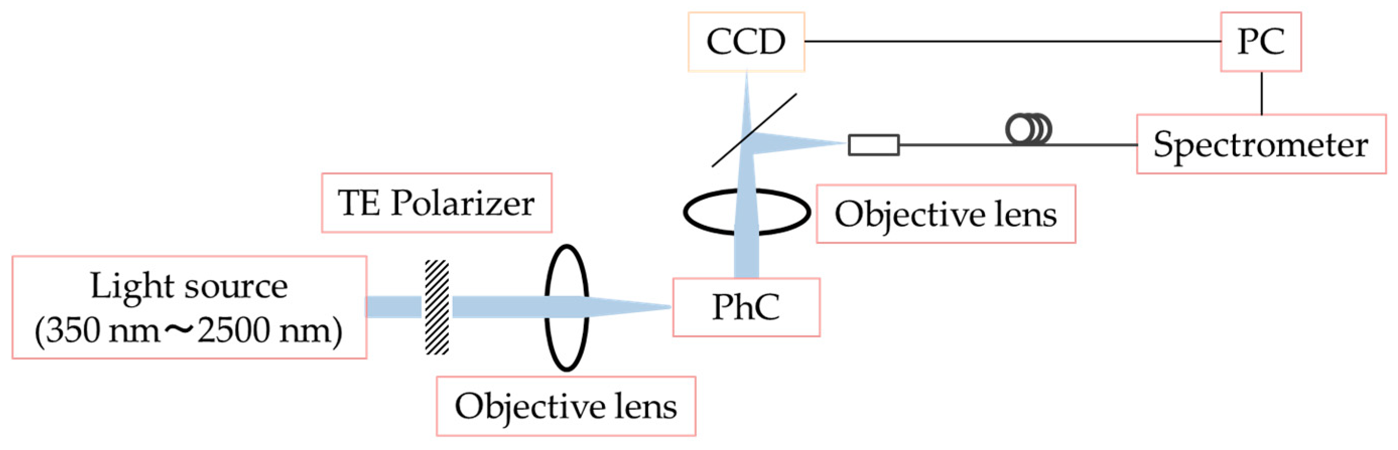
2.2. Apparatus
2.3. Method
2.3.1. Simulation Analysis
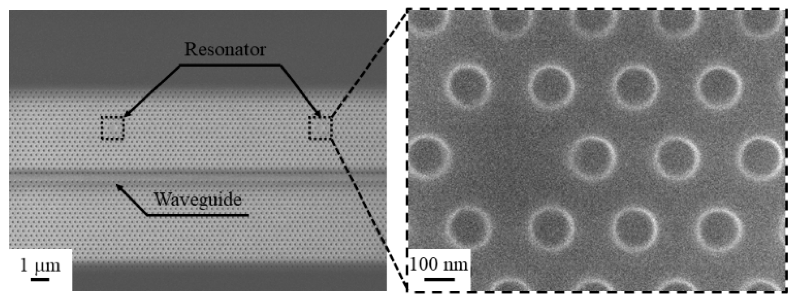
2.3.2. Fabrication of PhC Using Electron Beam Lithography
2.3.3. Evaluation of PhC Resonator and Waveguide
3. Results
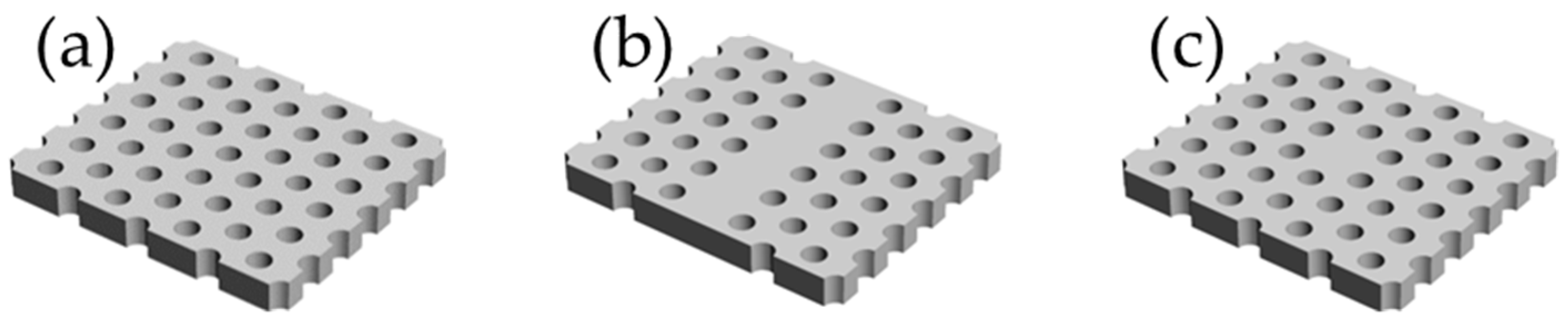
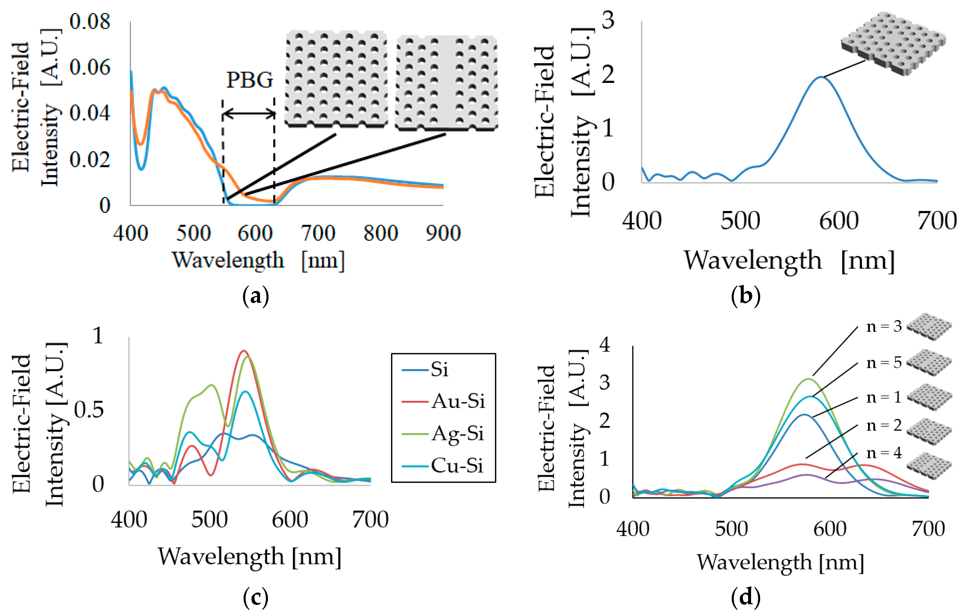
3.1. Simulation
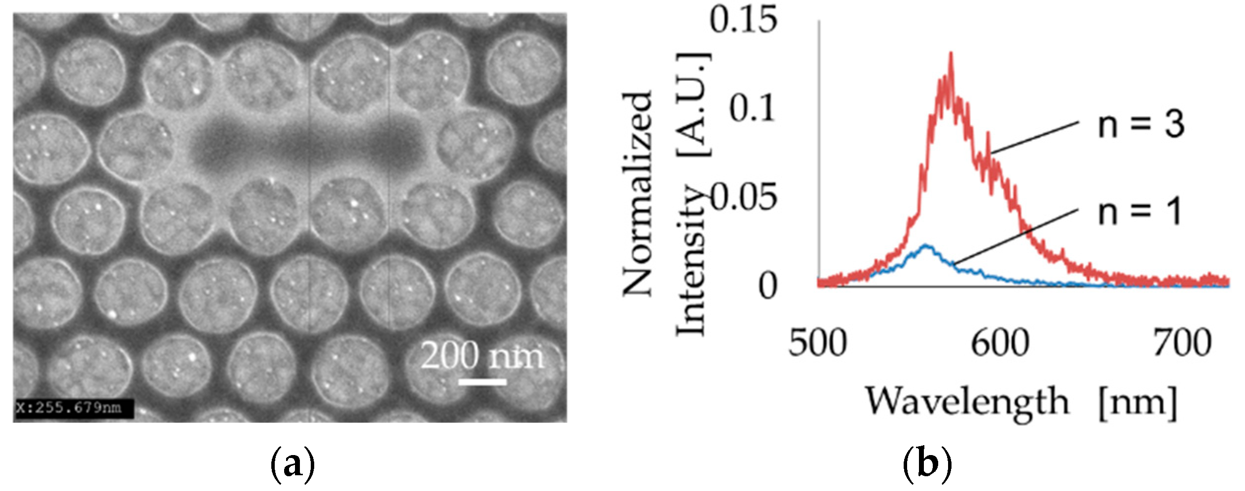
3.2. Fabrication of PhC
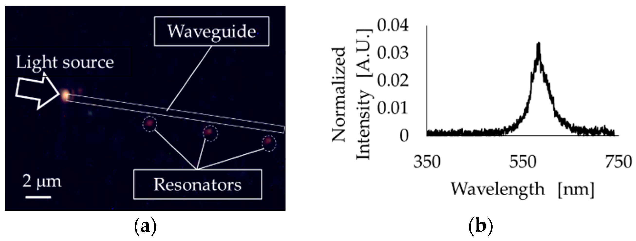
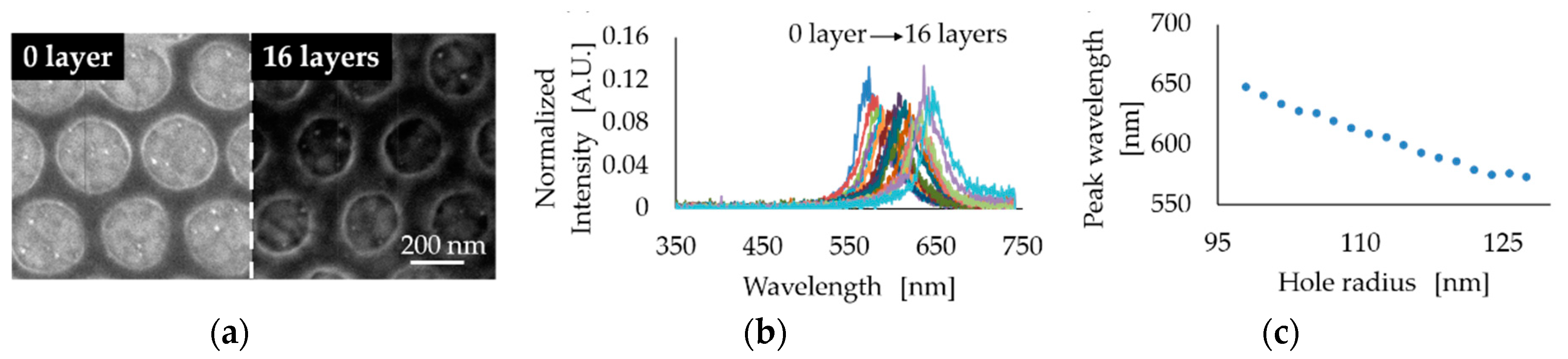
3.3. Microscopic Observation and Measurements
4. Conclusions
Author Contributions
Funding
Conflicts of Interest
References
- Yablonovitch, E. Inhibited Spontaneous Emission in Solid-State Physics and Electronics. Phys. Rev. Lett. 1987, 58, 2059–2062. [Google Scholar] [CrossRef] [PubMed]
- John, S. Strong Localization of Photons in Centain Disordered Dielectric Superlattices. Phys. Rev. Lett. 1987, 58, 2486–2489. [Google Scholar] [CrossRef] [PubMed]
- Gomyo, A.; Ushida, J.; Shirane, M. Highly drop-efficient channel-drop optical filters with Si-based photonic crystal slabs. Thin Solid Films 2006, 508, 422–425. [Google Scholar] [CrossRef]
- Chien, H.D.; Chen, C.C.; Luan, P.G. Photonic crystal beam splitters. Opt. Commun. 2006, 259, 873–875. [Google Scholar] [CrossRef]
- Aki, S.; Endo, T.; Sueyoshi, K.; Hisamoto, H. Plasticized poly (vinyl chloride)-based photonic crystal for ion sensing. Anal. Chem. 2014, 86, 11986–11991. [Google Scholar] [CrossRef] [PubMed]
- Lee, K.; Asher, S.A. Photonic Crystal Chemical Sensors: PH and Ionic Strength. J. Am. Chem. Soc. 2000, 122, 9534–9537. [Google Scholar] [CrossRef]
- Huang, M.; Yanik, A.A.; Chang, T.; Altug, H. Sub-wavelength nanofluidics in photonic crystal sensors. Opt. Express 2009, 17, 24224–24233. [Google Scholar] [CrossRef] [PubMed]
- Zhao, Y.; Zhang, Y.; Wang, Q. High sensitivity gas sensing method based on slow light in photonic crystal waveguide. Sens. Actuators B Chem. 2012, 173, 28–31. [Google Scholar] [CrossRef]
- Emami, H.; Alidadi, M.; Heidari, A.E.; Herdari, M.E. Optimizing of rod-type photonic crystal waveguide methane gas sensor. Optik 2016, 127, 2461–2466. [Google Scholar] [CrossRef]
- Buswell, S.C.; Wright, V.A.; Buriak, J.M.; Van, V.; Evoy, S. Specific detection of proteins using photonic crystal waveguides. Opt. Express 2008, 16, 15949–15957. [Google Scholar] [CrossRef] [PubMed]
- Ruperez, J.G.; Toccafondo, V.; Banuls, M.J.; Castello, J.G.; Griol, A.; Llopis, S.P.; Maquieira, A. Label-free antibody detection using band edge fringes in SOI planar photonic crystal waveguides in the slow light regime. Opt. Express 2010, 18, 24276–24286. [Google Scholar] [CrossRef] [PubMed]
- No, Y.; Ee, H.; Kwon, S.; Kim, S.; Seo, M.; Kang, J.; Lee, Y.; Park, H. Characteristics of dielectric-band modified single-cell photonic crystal lasers. Opt. Express 2009, 17, 1679–1690. [Google Scholar] [CrossRef] [PubMed]
- Hagemeier, J.; Bonato, C.; Truong, T.; Kim, H.; Beirne, G.J.; Bakker, M.; Exter, M.P.; Luo, Y.; Petroff, P.; Bouwmeester, D. H1 photonic crystal cavities for hybrid quantum information protocols. Opt. Express 2012, 20, 24714–24726. [Google Scholar] [CrossRef] [PubMed]
- Pal, S.; Yadav, A.R.; Lifson, M.A.; Baker, J.E.; Fauchet, P.M.; Miller, B.L. Selective virus detection in complex sample matrices with photonic crystal optical cavities. Biosens. Bioelectron. 2013, 44, 229–234. [Google Scholar] [CrossRef] [PubMed] [Green Version]
- Hachuda, S.; Watanabe, T.; Takahashi, D.; Baba, T. Sensitive and selective detection of prostatespecific antigen using a photonic crystal nanolaser. Opt. Express 2016, 24, 12886–12892. [Google Scholar] [CrossRef] [PubMed]
- Endoa, T.; Sato, M.; Kajita, H.; Okuda, N.; Tanaka, S.; Hisamoto, H. Printed two-dimensional photonic crystals for single-step label-free biosensing of insulin under wet conditions. Lab Chip 2012, 12, 1995–1999. [Google Scholar] [CrossRef] [PubMed]
- Endoa, T.; Ueda, C.; Kajita, H.; Okuda, N.; Tanaka, S.; Hisamoto, H. Enhancement of the fluorescence intensity of DNA intercalators using nano-imprinted 2-dimensional photonic crystal. Microchim. Acta 2013, 180, 929–934. [Google Scholar] [CrossRef]
- Terada, Y.; Hashimoto, W.; Endo, T.; Seto, H.; Murakami, Y.; Hisamoto, H. Signal amplified two-dimensional photonic crystal biosensor immobilized with glycol-nanoparticles. J. Mater. Chem. B 2014, 2, 3324–3332. [Google Scholar] [CrossRef]
- Hashimoto, W.; Endo, T.; Sueyoshi, K.; Hisamoto, H. Development of novel protease assay device using a nanoimprinted two dimensional photonic crystal. Chem. Lett. 2014, 43, 1728–1730. [Google Scholar] [CrossRef]
- Endo, T.; Yamamoto, K.; Sueyoshi, K.; Hisamoto, H. Development of Microchip Electrophoresis-Integrated Nanoimprinted Photonic Crystal. Sens. Mater. 2015, 27, 425–433. [Google Scholar] [CrossRef]
- Maeno, K.; Aki, S.; Sueyoshi, K.; Endo, T.; Hisamoto, H. Polymer-based Photonic Crystal Cavity Sensor for Optical Detection in the Visible Wavelength Region. Anal. Sci. 2016, 32, 117–120. [Google Scholar] [CrossRef] [PubMed] [Green Version]
- Endo, T.; Kajita, H.; Kawaguchi, Y.; Himi, T.K.T. Label-free optical detection of C-reactive protein by nanoimprint lithography-based 2D-photonic crystal film. Biotechnol. J. 2016, 11, 831–837. [Google Scholar] [CrossRef] [PubMed]
- Aki, S.; Sueyoshi, K.; Endo, T.; Hisamoto, H. Origin of the Optical Response of a Dye-doped Plasticized Poly (vinyl chloride)-based Photonic Crystal Ion Sensor. Anal. Sci. 2017, 33, 1247–1251. [Google Scholar] [CrossRef] [PubMed]
- Sun, J.; Maeno, K.; Aki, S.; Sueyoshi, K.; Endo, T.; Hisamoto, H. Design and Fabrication of Polymer-based Photonic Crystal Waveguide for Sensing Application. In Proceedings of the International Microprocesses and Nanotechnology Conference, Kyoto, Japan, 8–11 November 2016. [Google Scholar]
- Sukhorukov, G.B.; Donath, E.; Lichtenfeld, H.; Knippel, E.; Knippel, M.; Budde, A.; Mohwald, H. Layer-by-layer self assembly of polyelecrolytes on colloidal particles. Colloids Surf. A 1998, 137, 253–266. [Google Scholar] [CrossRef]
- Sun, J.; Maeno, K.; Aki, S.; Sueyoshi, K.; Endo, T.; Hisamoto, H. Fabrication of Polymer-based Photonic Crystal Waveguide with Nano-Cavities for Sensing Application. In Proceedings of the International Congress on Analytical Sciences, Haikou, China, 5–8 May 2017. [Google Scholar]
- Ladam, G.; Schaad, P.; Vogel, J.C.; Schaaf, P.; Decher, G.; Cuisinier, F. In Situ determination of the structural properties of initially deposited polyelectrolyte multilayers. Langmuir 2000, 16, 1249–1255. [Google Scholar] [CrossRef]
- Liang, F.; Guo, Y.; Hou, S.; Quan, Q. Photonic-plasmonic hybrid single-molecule nanosensor measures the effect of fluorescent labels on DNA-protein dynamics. Sci. Adv. 2017, 3, e1602991. [Google Scholar] [CrossRef] [PubMed]
- Liang, F.; Clarke, N.; Patel, P.; Loncar, M.; Quan, Q. Scalable photonic crystal chips for high sensitivity protein detection. Opt. Express 2013, 21, 32306–32312. [Google Scholar] [CrossRef] [PubMed]
- Liang, F.; Zhang, Y.; Hong, W.; Dong, Y.; Xie, Z.; Quan, Q. Direct tracking of amyloid and tau dynamics in neuroblastoma cells using nanoplasmonic fiber tip probes. Nano Lett. 2016, 16, 3989–3994. [Google Scholar] [CrossRef] [PubMed]
- Watanabe, K.; Kishi, Y.; Hachuda, S.; Watanabe, T.; Sakemoto, M.; Nishijima, Y.; Baba, T. Simultaneous detection of refractive index and surface charges in nanolaser biosensors. Appl. Phys. Lett. 2015, 106, 021106. [Google Scholar] [CrossRef]
- Endo, T.; Yanagida, Y.; Hatsuzawa, T. Colorimetric detection of volatile organic compounds using a colloidal crystal-based chemical sensor for environmental applications. Sens. Actuators B Chem. 2007, 125, 589–595. [Google Scholar] [CrossRef]
- Malinin, A.V.; Zanishevskaja, A.A.; Tuchin, V.V.; Skibina, Y.S.; Silokhin, I.Y. Photonic crystal fibers for food quality analysis. In Proceedings of the SPIE 8427, Biophotonics: Photonic Solutions for Better Health Care III, Brussels, Belgium, 8 May 2012. [Google Scholar]


© 2018 by the authors. Licensee MDPI, Basel, Switzerland. This article is an open access article distributed under the terms and conditions of the Creative Commons Attribution (CC BY) license (http://creativecommons.org/licenses/by/4.0/).
Share and Cite
Sun, J.; Maeno, K.; Aki, S.; Sueyoshi, K.; Hisamoto, H.; Endo, T. Design and Fabrication of a Visible-Light-Compatible, Polymer-Based Photonic Crystal Resonator and Waveguide for Sensing Applications. Micromachines 2018, 9, 410. https://doi.org/10.3390/mi9080410
Sun J, Maeno K, Aki S, Sueyoshi K, Hisamoto H, Endo T. Design and Fabrication of a Visible-Light-Compatible, Polymer-Based Photonic Crystal Resonator and Waveguide for Sensing Applications. Micromachines. 2018; 9(8):410. https://doi.org/10.3390/mi9080410
Chicago/Turabian StyleSun, Jiayi, Kenichi Maeno, Shoma Aki, Kenji Sueyoshi, Hideaki Hisamoto, and Tatsuro Endo. 2018. "Design and Fabrication of a Visible-Light-Compatible, Polymer-Based Photonic Crystal Resonator and Waveguide for Sensing Applications" Micromachines 9, no. 8: 410. https://doi.org/10.3390/mi9080410