1. Introduction
Magnetic field (MF) sensors, which are important components, are applied in industrial apparatuses, automation equipment, cable-stayed bridges, electrical devices and portable electronic instruments [
1,
2,
3,
4]. Traditional MF sensors [
5,
6], which were not manufactured by microfabrication, were not only large volume, but also high cost. The advantages of micro magnetic field (MMF) sensors are small volume and low cost. Micro-electro-mechanical-system (MEMS) technology could be utilized to fabricate micro sensors [
7,
8,
9,
10,
11]. Several MMF sensors were manufactured using MEMS technology. For instance, Mian [
12] developed resonant MMF sensors fabricated by the surface micromachining process. The sensor structure contained microbeams and a membrane, the material of which was a stack of double polysilicon layers. Based on the Lorentz force principle, the MMF caused a capacitance change upon sensing an MF. The Lorentz force resonant MEMS magnetic field sensors were proposed by Park [
13]. The MMF sensors had a micromirror actuated by the Lorentz force that was generated using a sinusoidal current and an incident MF. The rotation angle of the micromirror was recorded using an optical measurement. Dennis [
14] used a CMOS process to manufacture resonant MMF sensors. The sensor was fabricated using the stacked layers of the CMOS process, and a post-CMOS processing with reactive ion etch (RIE) dry etching was adopted, releasing the device structure. The sensor shuttle was excited using the Lorentz force and external MF, and the resonance amplitude was detected by an optical instrument. These resonant MMF sensors [
12,
13,
14] required movable suspension structures, so sacrificial layer technology was used to release the suspension structures. For example, after completion of the CMOS process, the resonant MMF sensors, proposed by Dennis [
14], used an RIE dry etching post-processing to obtain the suspension structures of the devices. In this work, we design a magnetotransistor/Hall element MMF sensor without a suspension structure using a CMOS process, so the sensor does not need post-CMOS processing. Therefore, the sensor fabrication in this work is easier than that of these sensors [
12,
13,
14].
A one-axis magnetotransistor MMF sensor, presented by Tseng [
15], was fabricated by a standard 0.18-μm CMOS process of Taiwan Semiconductor Manufacturing Company (TSMC). The MMF sensor had a sensitivity of 354 mV/T. Furthermore, Tseng [
16] adopted the same method to design a three-axis magnetotransistor MMF sensor that was also made using a standard 0.18-μm CMOS process of TSMC. The MMF sensor had a sensitivity of 6.5 mV/T in the x-axis and a sensitivity of 0.4 mV/T in the y-axis. A two-dimensional Hall MMF sensor with a lateral magnetotransistor and magnetoresistor, developed by Yu [
17], was produced using a standard 0.35-μm CMOS process. The sensitivity of the MMF sensor was 0.385 V/(A·T) at a bias current of 100 mA. Sung [
18] proposed a two-dimensional Hall MMF sensor manufactured utilizing a standard 0.35-μm CMOS process. The MMF sensor was composed of a bulk magnetotransistor, a vertical magnetoresistor and a vertical magnetotransistor. The sensitivity of the sensor was 1.92 V/(A·T) at a bias current of 20 mA. With the same design method, Sung [
19] developed a three-dimensional Hall MMF sensor with a bandgap reference and readout circuit made using a standard 0.18-μm CMOS process. The MMF sensor contained one-dimensional lateral Hall sensor and a two-dimensional vertical Hall sensor. The MMF sensor had a sensitivity of 5943 V/(A·T) at a bias current of 6.25 mA in the x- and y-axis MF and a sensitivity of 14,790 V/(A·T) at a bias current of 6.25 mA in the z-axis MF. The Hall MMF sensors, proposed by Xu [
20], were fabricated by the 0.18-μm high voltage (HV) CMOS process for sensing low MF. The sensors consisted of a Hall plate with a switching cross-shape. Zhao [
21] utilized a CMOS process to make nano-polysilicon transistor MMF sensors. A nano-polysilicon/single silicon junction was adopted as a sensing layer. The nano-polysilicon transistors were fabricated on silicon substrate with high resistivity. The two-dimensional MMF sensors, develop by Yang [
22], included four magnetic transistors. The MMF sensors were manufactured on a high resistivity silicon wafer using microfabrication technology, and they were packaged on printed circuit boards. The sensor sensitivity in the x-axis was 366 mV/T, and its sensitivity in the y-axis was 365 mV/T, respectively. These micro sensors [
15,
17,
20,
21,
22] manufactured using CMOS technology were one-axis and two-axis MMF sensors. Therefore, three-axis MMF sensors in this work are fabricated using a standard 0.18-μm CMOS process of TSMC, and the sensitivity of the sensors is higher than that of Tseng [
16].
Various MEMS actuators and sensors, which are manufactured utilizing a CMOS process, are called CMOS-MEMS devices [
23,
24,
25,
26,
27]. We adopt CMOS-MEMS technology to develop three-axis MMF sensors. MMF sensors are composed of a magnetotransistor and four Hall elements. The magnetotransistor is designed to detect MF in the x-axis and y-axis. Four Hall elements are designed to sense MF in the z-axis. These CMOS-MEMS magnetic field sensors [
28,
29,
30] needed a post-CMOS processing [
31] to form suspension structures. The fabrication of the MMF sensors in this study is consistent with the CMOS process and does not need post-CMOS processing.
2. Structure of MMF Sensor
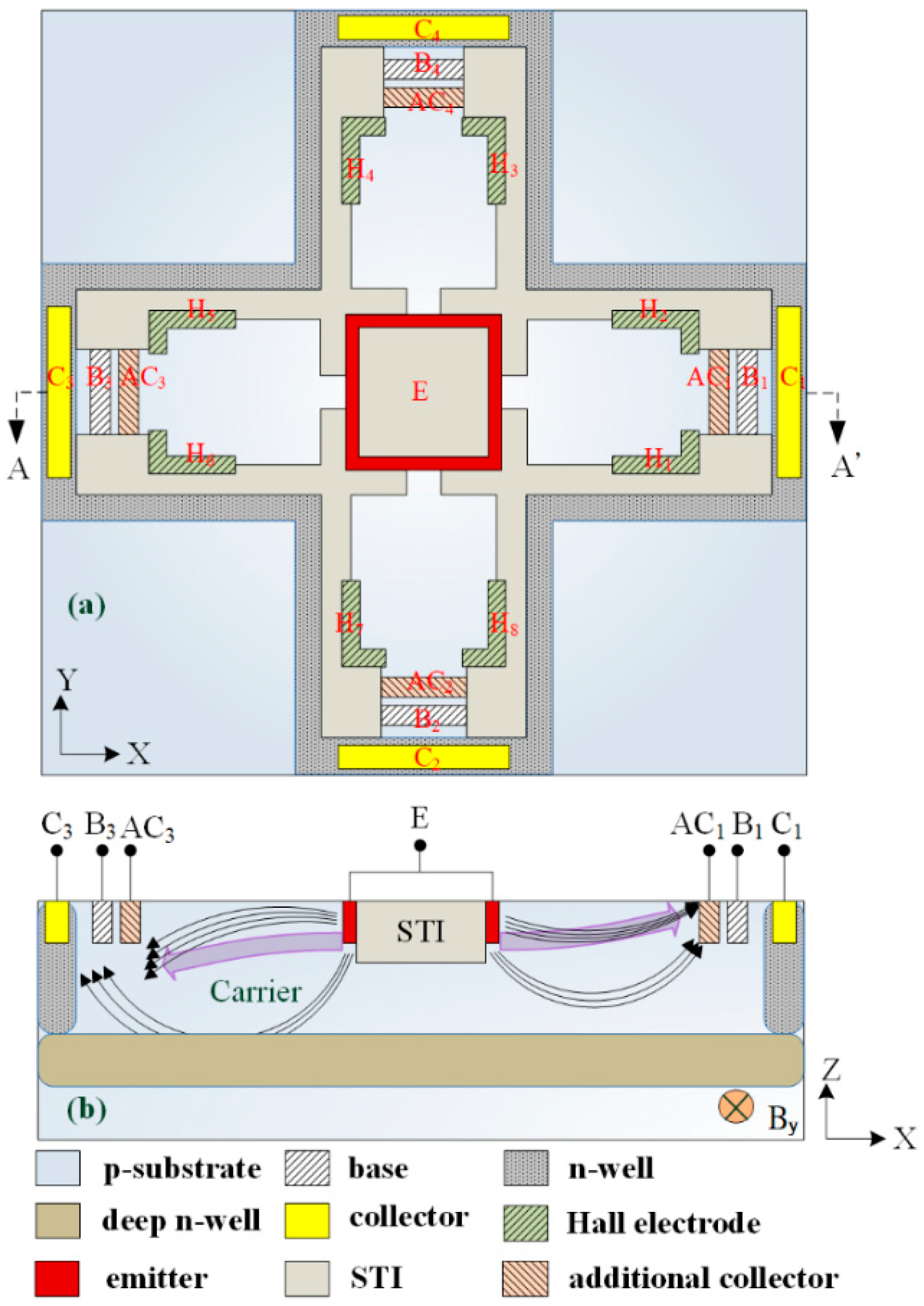
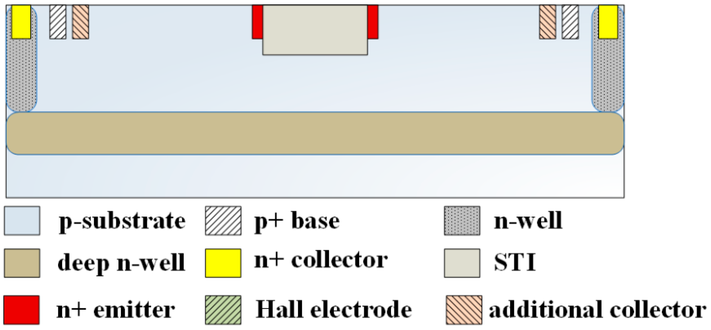
Figure 1a demonstrates the MMF sensor structure, where E denotes the emitter, B
1, B
2, B
3 and B
4 are the bases, C
1, C
2, C
3 and C
4 are the collectors, AC
1, AC
2, AC
3 and AC
4 are the additional collectors and H
1, H
2, H
3, H
4, H
5, H
6, H
7 and H
8 are the electrodes of the Hall elements.
The MMF sensor includes a magnetotransistor and four Hall elements. The magnetotransistor is employed to detect MF in the x-axis and y-axis, and the four hall elements are utilized to sense MF in the z-axis. In addition to the emitter, bases and collectors, the additional collectors are introduced into the magnetotransistor. The additional collectors can increase bias current, so that the emitter induces more electron carriers. Shallow trench isolation (STI) oxide is used to confine the current direction, so that leakage current reduces.
Figure 2 illustrates the equivalent circuit for the magnetotransistor, where R represents the resister, V
C1, V
C2, V
C3 and V
C4 are the bias voltage of the collectors, V
AC1, V
AC2, V
AC3 and V
AC4 are the bias voltage of the additional collectors, V
B1, V
B2, V
B3, and V
B4 are the bias voltage of the bases, V
out-AC1, V
out-AC2, V
out-AC3 and V
out-AC4 are the output voltages and the symbol (4) denotes the corresponding circuit repeated four times.
Figure 1b demonstrates a cross-sectional view of the MMF sensor. The sensing mechanism of the magnetotransistor is explained as follows. As shown in
Figure 1b, when the bias voltages are applied to the collectors, the bases and the additional collectors, carriers produce a movement from the emitter to the additional collectors AC
1/AC
3, the bases B
1/B
3 and the collectors C
1/C
3. Given a magnetic field in the y-axis, carriers (on the right in
Figure 1b) are bent upward because of the action of the Lorentz force. The carriers have difficulty passing across the additional collector AC
1 to the base B
1 and collector C
1. Most of carriers move to the additional collector AC
1, resulting in the current increment of the additional collector AC
1. At the same time, carriers (on the left in
Figure 1b) are bent downward owing to the action of the Lorentz force. Most of the carriers move across the additional collector AC
3 to the base B
3 and collector C
3, leading to the current decrement of the additional collector AC
3. Therefore, this action produces a voltage difference between the additional collectors AC
1 and AC
3 in the y-direction MF. As shown in
Figure 2, the additional collectors AC
1 and AC
3 respectively connect to a resistor R, so the voltage difference of the additional collectors AC
1 and AC
3 is obtained by V
out-AC1 − V
out-AC3, which is the sensor output voltage in the y-axis MF. Similarly, when the bias voltages are applied to the collectors, the bases and the additional collectors, carriers produce a movement from the emitter to the additional collectors AC
2/AC
4, the bases B
2/B
4 and the collectors C
2/C
4. Given a magnetic field in the x-axis, carriers that move to the additional collector AC
2 are bent downward by Lorentz force, leading to the current decrement of the additional collector AC
2. Additionally, carriers that move to the additional collector AC
4 are bent upward by the Lorentz force, resulting in the current increment of the additional collector AC
4. The current between both additional collectors AC
2 and AC
4 generates an imbalance, so the additional collectors AC
2 and AC
4 produce a voltage difference. As shown in
Figure 2, the voltage difference of the additional collectors AC
2 and AC
4 can be obtained by V
out-AC4 − V
out-AC2, which is the sensor output voltage in the x-axis MF.
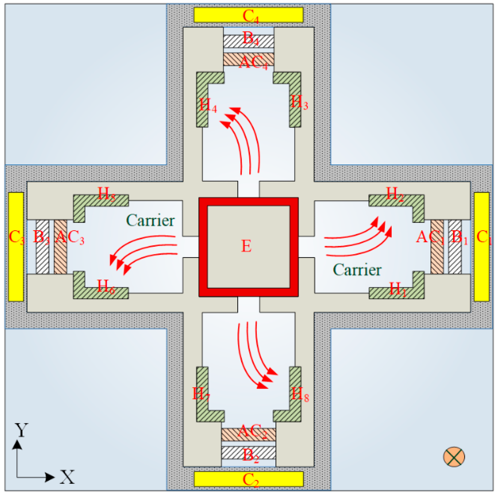
The MMF sensor has four Hall elements used to detect z-direction MF.
Figure 3 presents the carriers’ path in the MMF sensor under z-direction MF. As shown in
Figure 3, when the bias voltages are applied to the collectors, bases and additional collectors, carriers cause a movement from the emitter to the additional collectors AC
1, AC
2, AC
3 and AC
4. Given an MF in the z-axis, carriers are bent toward the Hall electrodes H
1, H
3, H
5 and H
7 by the Lorentz force. The current causes an imbalance between the electrodes H
1 and H
2, leading to the generation of a Hall voltage between the electrodes H
1 and H
2. Similarly, the Hall voltages between the electrodes H
3/H
4, H
5/H
6 and H
7/H
8, respectively, are generated in z-direction MF. The Hall voltages in series are the sensor output voltages in z-axis MF.
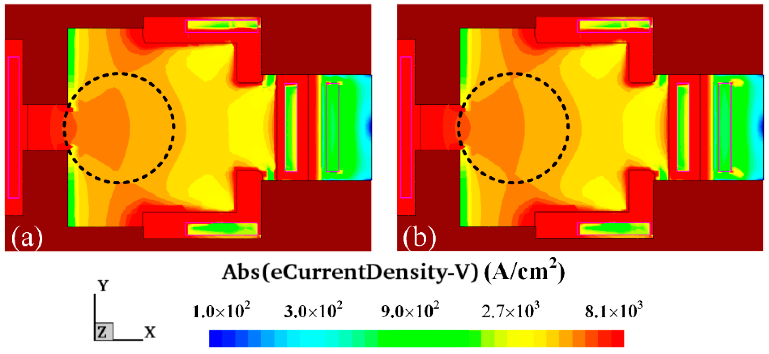
The Sentaurus TCAD, which is a finite element method software, was utilized to simulate the MMF sensor performance. According to the structure in
Figure 1a, the model of the MMF sensor was constructed. To save computation time, one-quarter of the MMF model was established because the MMF sensor structure was symmetric. Then the method of Delaunay triangulation was employed to mesh the MMF model. The approach of the Poisson electron hole was used to compute the coupling effect of MF and the electrical field, and the method of Bank/Rose was utilized to solve the carrier density distribution of the MMF sensor.
In this simulation, bias voltages of 1.5 V, 4.5 V and 4.5 V were supplied to bases, collectors and additional collectors, respectively. A magnetic field of 250 mT was given in the y-axis.
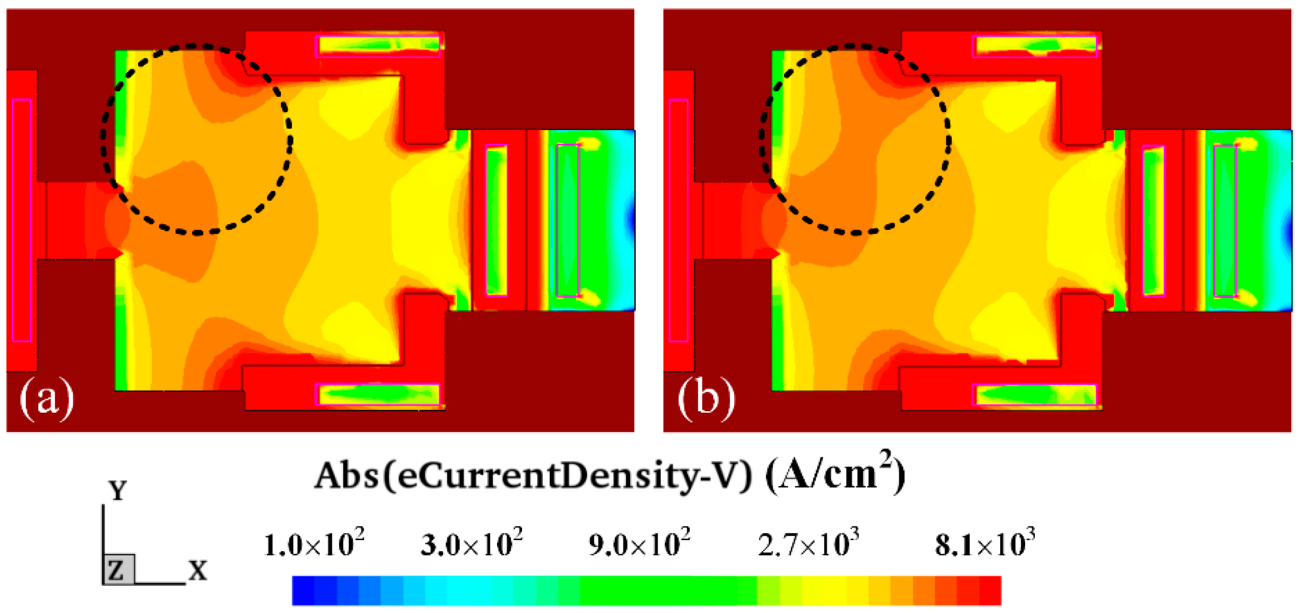
Figure 4 shows the simulated carrier density distribution of the MMF sensor under the y-direction magnetic field.
Figure 4a illustrates the carrier density distribution of the MMF sensor without a magnetic field.
Figure 4b reveals the carrier density distribution of the MMF sensor with a magnetic field of 250 mT in the y-axis. By the comparison of the simulated results in
Figure 4a,b, the current density of the path from the emitter to the additional collector increases.
The carrier density distribution of the MMF sensor in the z-direction magnetic field was computed with the same simulation approach. In this computation, bias voltages of 1.5 V, 4.5 V and 4.5 V were supplied to bases, collectors and additional collectors, respectively. A magnetic field of 250 mT was applied in the z-axis.
Figure 5 shows the simulated carrier density distribution of the MMF sensor under the z-direction magnetic field.
Figure 5a demonstrates the carrier density distribution of the MMF sensor without a magnetic field.
Figure 5b presents the surface carrier density distribution of the MMF sensor with a magnetic field of 200 mT in the z-axis. As illustrated in
Figure 5a,b, carriers are bent toward the top Hall electrode.
4. Results
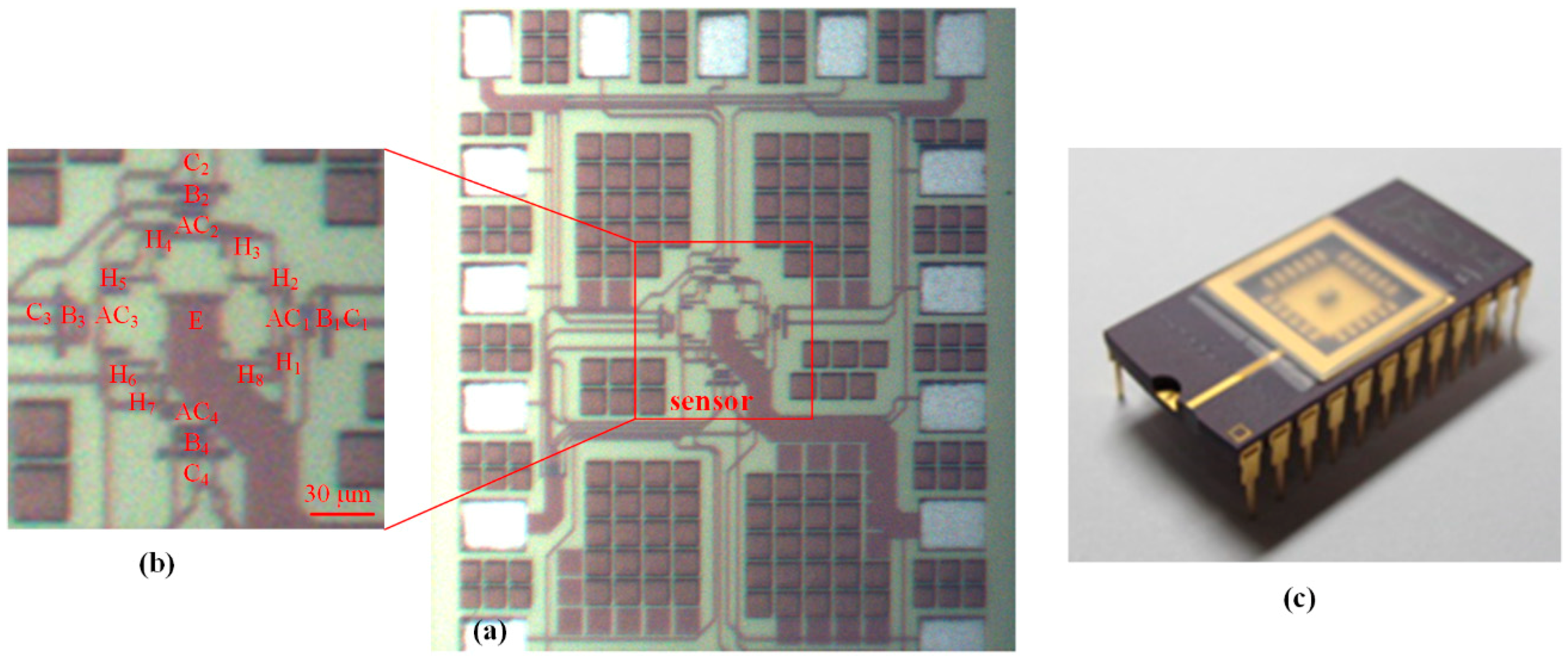
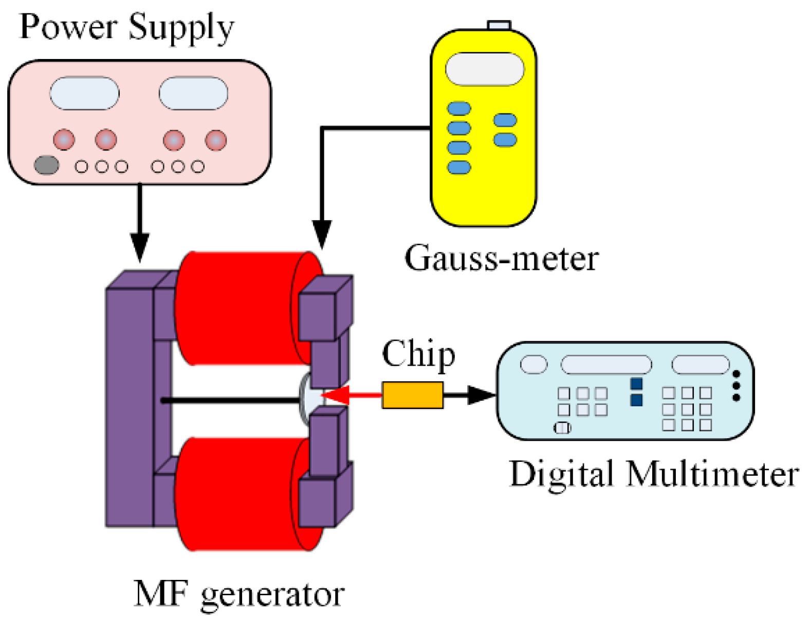
A magnetic testing system was employed to measure the MMF sensor performance.
Figure 8 demonstrates a magnetic testing system [
15], and the system includes a Gauss-meter (GM08-1029, Hirst, Falmouth, U.K.), an MF generator (developed by our lab), a power supply (GPC-3030DQ, Gwinstek, New Taipei City, Taiwan) and a digital multimeter (34405A, Agilent, Santa Clara, CA, USA). The magnetic generator was employed to generate an MF to test the MMF sensor. The power supply was used to provide power to the MF generator. The Gauss-meter was used to test the magnetic magnitude excited by the MF generator. The digital multimeter was utilized to record the MMF sensor output voltage.
The MMF sensor was composed of a magnetotransistor and four Hall elements. The magnetotransistor was used to detect MF in the x- and y-directions, and the Hall elements were utilized to measure the magnetic field in the z-direction. First, the MMF sensor performance in the x-direction MF was tested. The MMF sensor was set in the magnetic testing system. An MF range of −220–220 mT generated by the MF generator was supplied to the MMF sensor, and the MF magnitude was calibrated using the Gauss-meter. Bias voltages were applied to the bases, collectors and additional collectors. An MF in the y-direction was applied to the MMF sensor. The digital multimeter measured the voltage difference of the additional collectors AC
1/AC
3 in the MMF sensor.
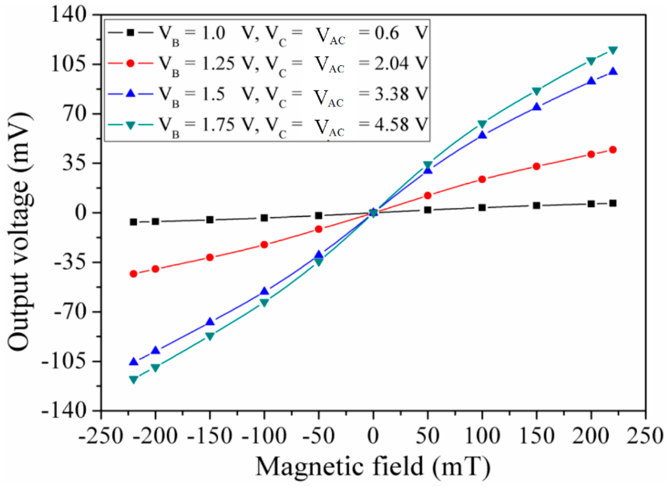
Figure 9 depicts the measured output voltage of the MMF sensor in the y-direction MF. When V
B = 1 V, V
C = 0.6 V and V
AC = 0.6 V, the sensor was insensitive to MF. The sensor became more sensitive to MF at V
B = 1.25 V, V
C = 2.04 V and V
AC =2.04 V, and its output voltage changed from −43.7 mV at −220 mT to 38.6 mV at 220 mT. When V
B = 1.5 V, V
C = 3.38 V and V
AC = 3.38 V, the sensor output voltage obviously increased under different MF. When V
B = 1.75 V, V
C = 4.58 V and V
AC = 4.58 V, the sensor output voltage varied from −120 mV at −220 mT to 119 mV at 220 mT, and the method of least squares was adopted to evaluate the linear regression of the curve. The evaluation obtained that the regression line had a slope of 0.55 V/T and a standard deviation of 5.4 mV. Thereby, the MMF sensor sensitivity in the y-direction MF was 0.55 V/T at bias voltage V
B = 1.75 V, V
C = 4.58 V and V
AC = 4.58 V.
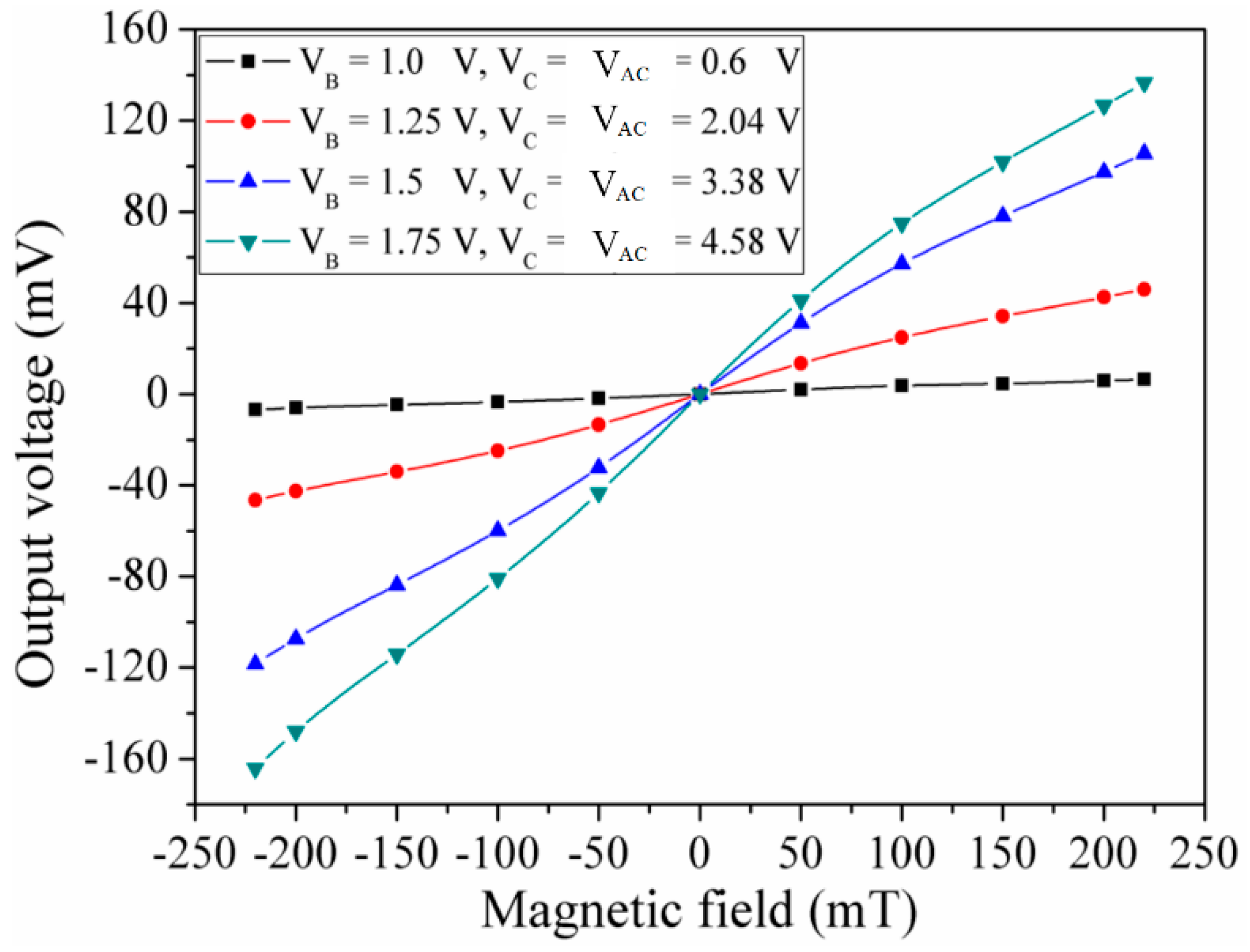
With the same testing approach, the sensing performance of the MMF sensor in the x-direction MF was measured. A MF in the x-direction was applied to The MMF sensor. The digital multimeter recorded the voltage difference of the additional collectors AC
2/AC
4 in the MMF sensor.
Figure 10 demonstrates the measured output voltage of the MMF sensor in the x-direction MF. The sensor was insensitive to MF at V
B = 1 V, V
C = 0.6 V and V
AC = 0.6 V. The sensor was more sensitive to MF at V
B = 1.25 V, V
C = 2.04 V and V
AC = 2.04 V, and it output voltage varied from −46.8 mV at −220 mT to 39 mV at 220 mT. When V
B = 1.5 V, V
C = 3.38 V and V
AC = 3.38 V, the output voltage enlarged under different MF. When V
B = 1.75 V, V
C = 4.58 V and V
AC = 4.58 V, the output voltage changed from −162 mV at −220 mT to 140 mV at 220 mT, and the method of least squares was used to calculate the linear regression of the curve. The calculation obtained that the regression line had a slope of 0.69 V/T and a standard deviation of 12 mV. Thereby, the MMF sensor sensitivity in the x-direction MF was 0.69 V/T at bias voltage V
B = 1.75 V, V
C = 4.58 V and V
AC = 4.58 V.
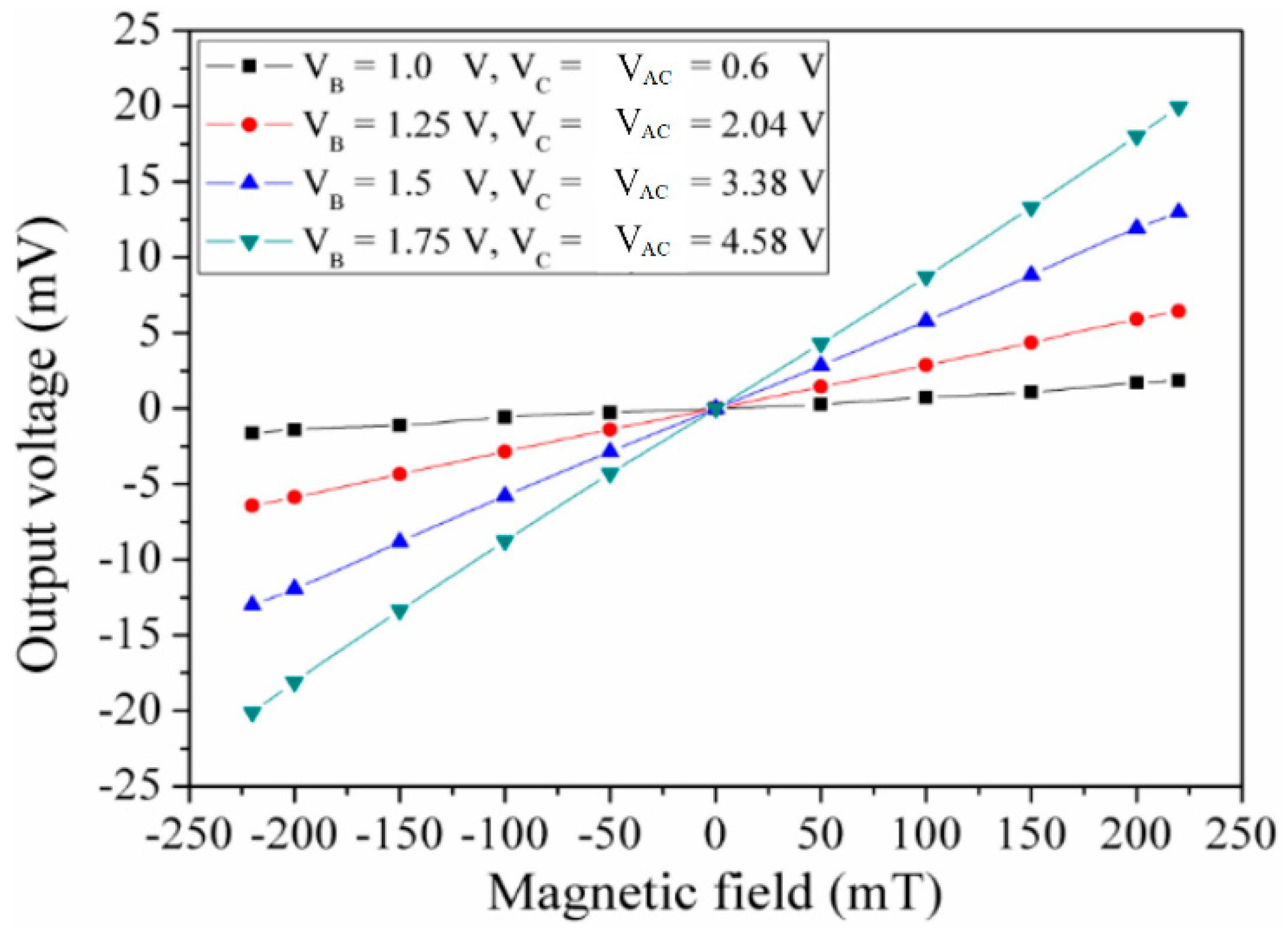
The sensing performance of the MMF sensor in the z-direction MF was tested. An MF in the z-direction was applied to the MMF sensor. The digital multimeter measured the output voltage of the Hall electrodes in the MMF sensor. The Hall voltage of the MMF sensor in the z-direction MF was recorded.
Figure 11 presents the measured output voltage of the MMF sensor in the z-direction MF. The MMF sensor was also insensitive to MF at V
B = 1 V, V
C = 0.6 V and V
AC = 0.6 V. When bias voltage V
B, V and V
AC increased, the sensor output voltage became large. When V
B = 1.75 V, V
C = 4.58 V and V
AC = 4.58 V, the MMF sensor output voltage varied from −20.5 mV at −220 mT to 20 mV at 220 mT, the curve slope of which was about 0.09 V/T. Thereby, the MMF sensor sensitivity in the z-direction MF was 0.09 V/T at bias voltage V
B = 1.75 V, V
C = 4.58 V and V
AC = 4.58 V.
The characteristics of the MMF sensor in the x- and y-direction MF should be the same owing to the MMF sensor being a symmetric structure. Actually, as shown in
Figure 9, the measured sensitivity of the MMF sensor in the y-direction MF was 0.55 V/T. There is little difference in the sensitivity of the MMF sensor in the x- and y-direction MF. The reason is due to packaging and fabrication deviation. As shown in
Figure 11, the curves were linear, because the sensing mechanism of the MMF sensor in the z-axis MF was based on the Hall elements. The Hall voltage, which was the output voltage of the sensor in the z-axis MF, was proportional to the magnetic field according to the sensing principle of the Hall element [
20]. On the other hand, the sensing mechanism of the MMF sensor in the x- and y-axis MF was based on the magnetotransistor. The carrier current density (
Figure 3) of the magnetotransistor depended on the magnetic field, and the I-V (current-voltage) characteristic of magnetotransistor was nonlinear [
15], so that the output voltage versus magnetic field (
Figure 9 and
Figure 10) of the MMF sensor in the x- and y-axis MF was nonlinear.
Table 1 shows a list of sensitivity for various MMF sensors fabricated by CMOS technology. The MMF sensors presented by Tseng [
15], Xu [
20] and Zhao [
21] were one-axis MF sensing, and the sensors proposed by Yu [
17], Sung [
18] and Yang [
22] were two-axis MF sensing. As depicted in
Table 1, the sensitivity of the MMF sensor in this work along the x- and y-axis MF exceeds that of Tseng [
16], Yu [
17], Sung [
18] and Yang [
22]. The sensitivity of the sensor presented by Zhao [
21] along the z-axis MF is higher than that of this work.


