Improving the Electrical Contact Performance for Amorphous Wire Magnetic Sensor by Employing MEMS Process


Abstract
:1. Introduction
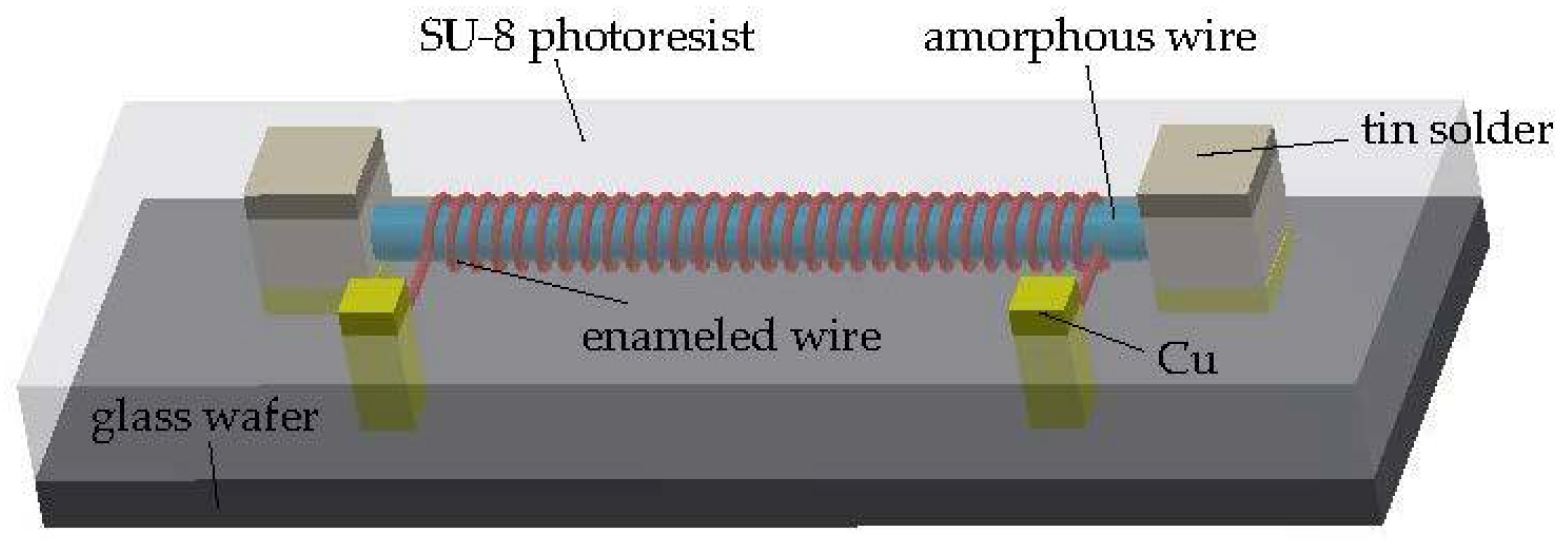
2. Device Design
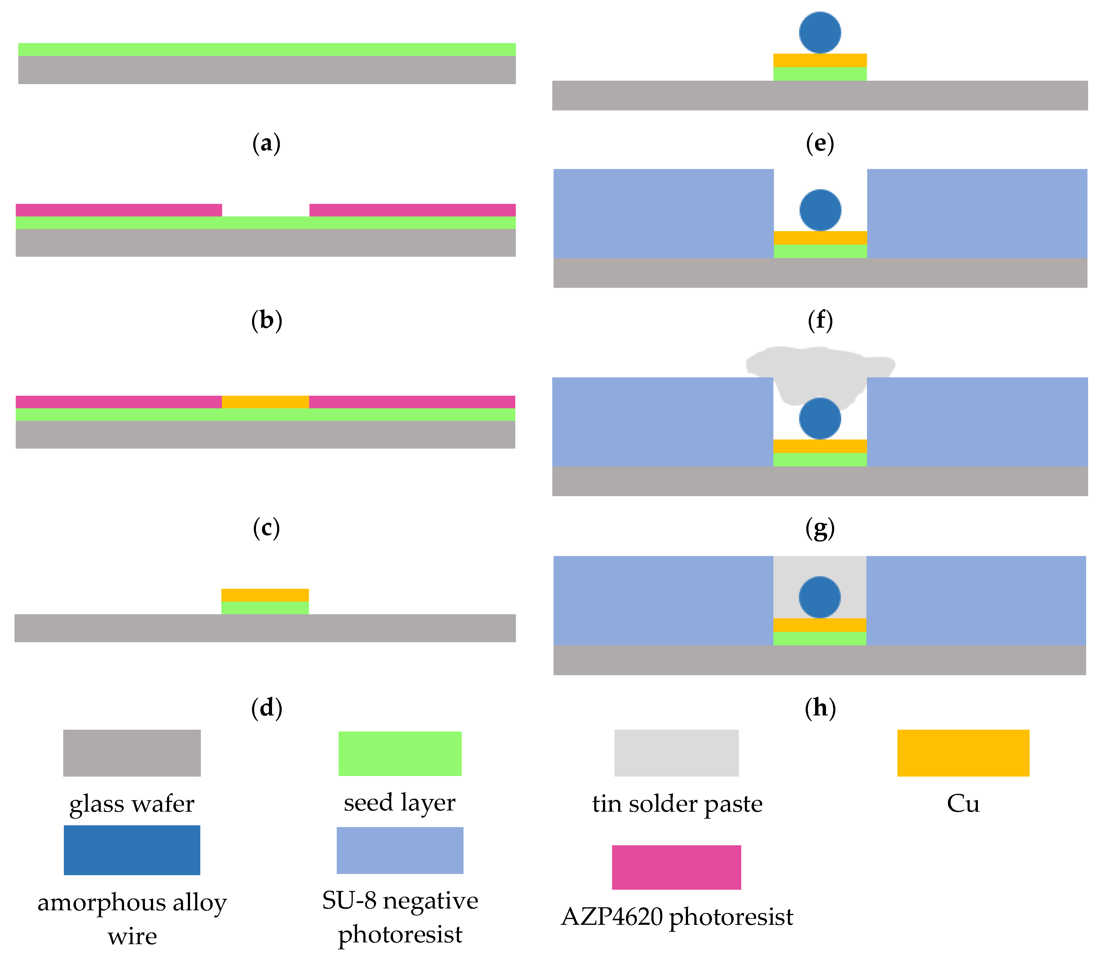
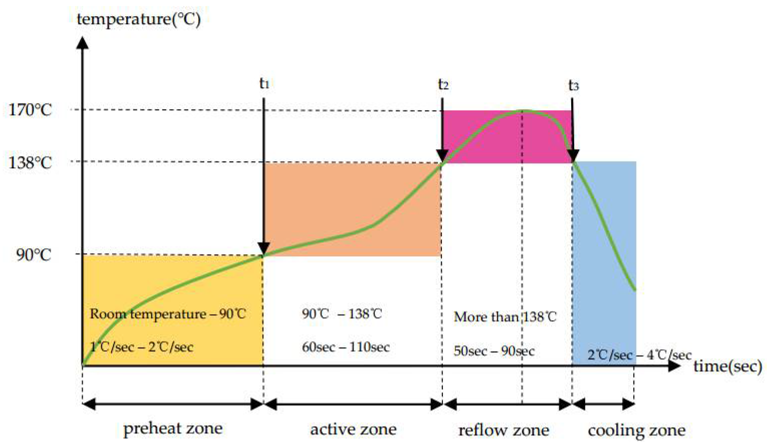
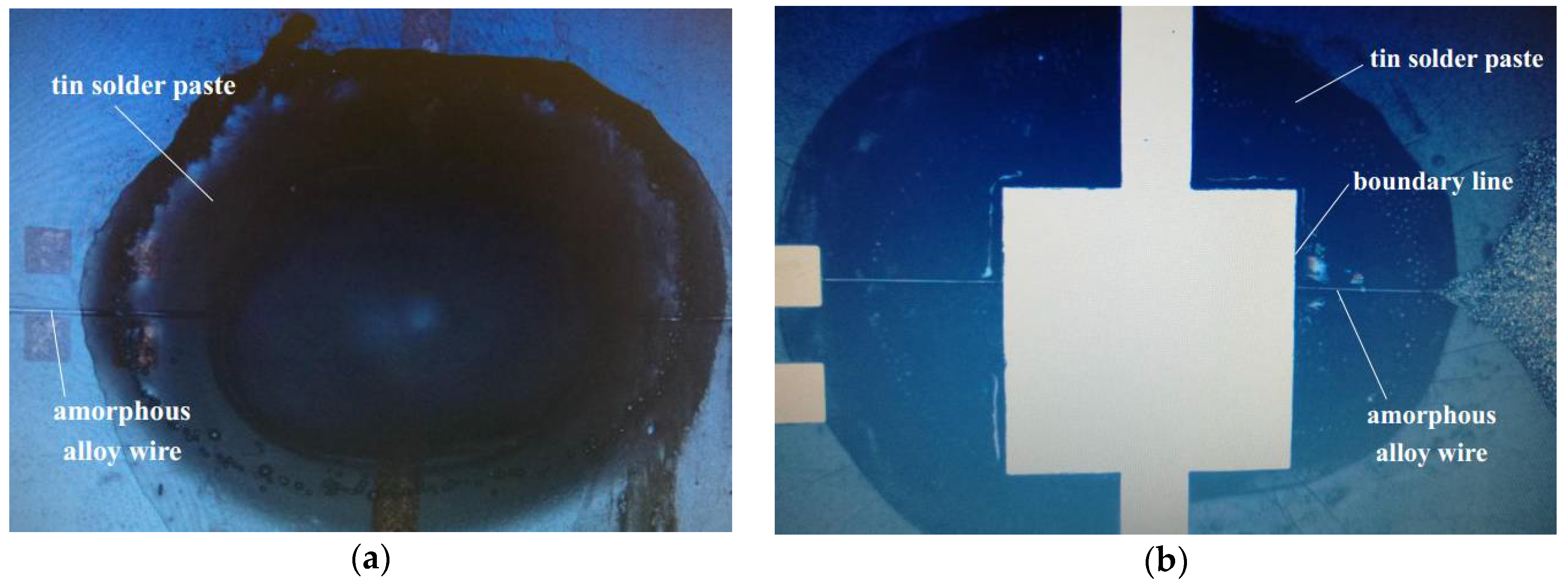
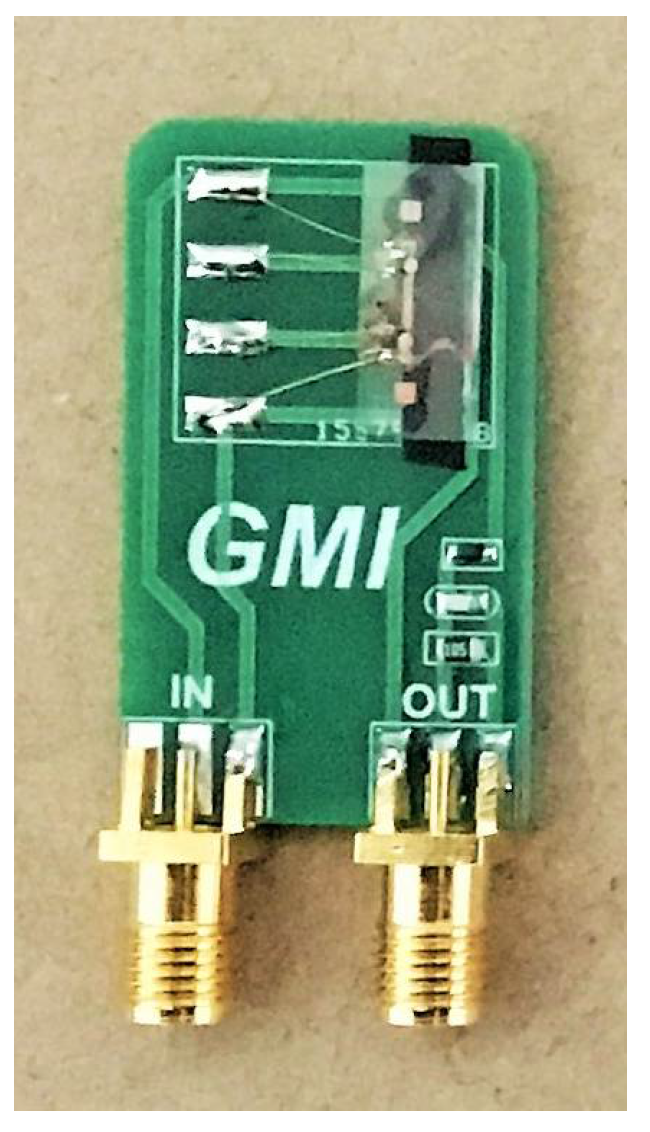
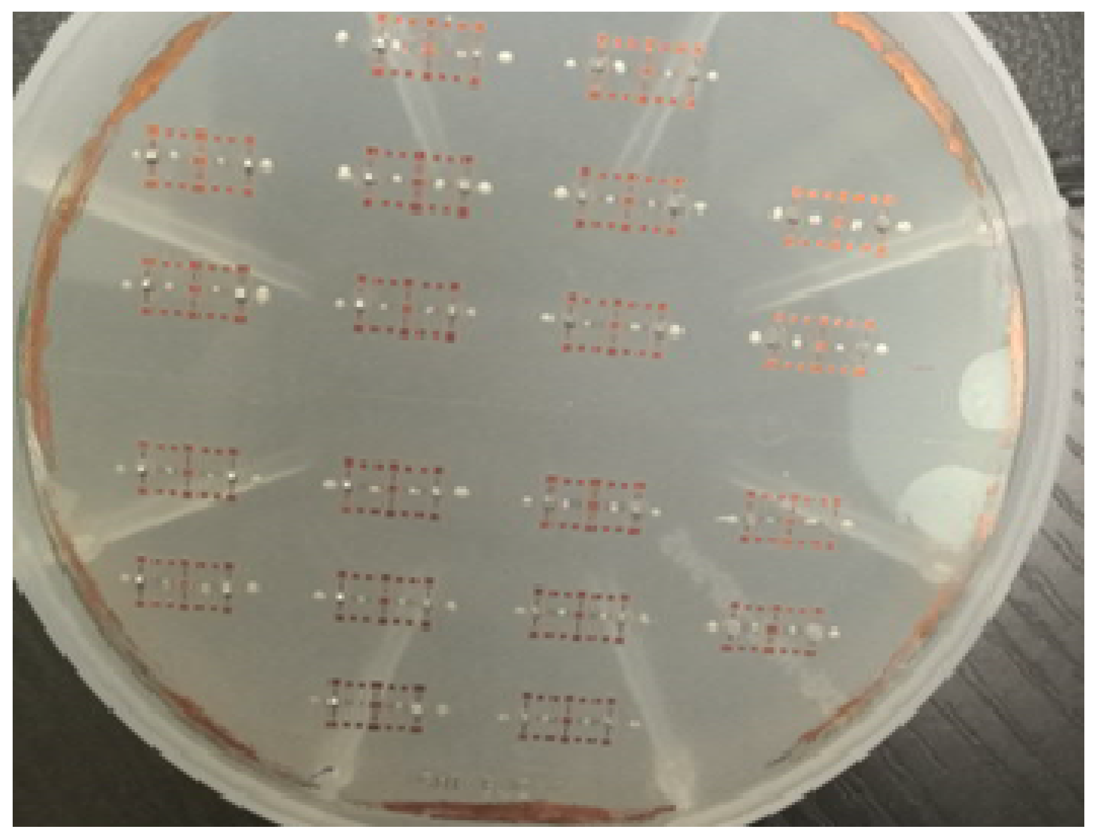
3. Device Fabrication
4. Results and Discussion
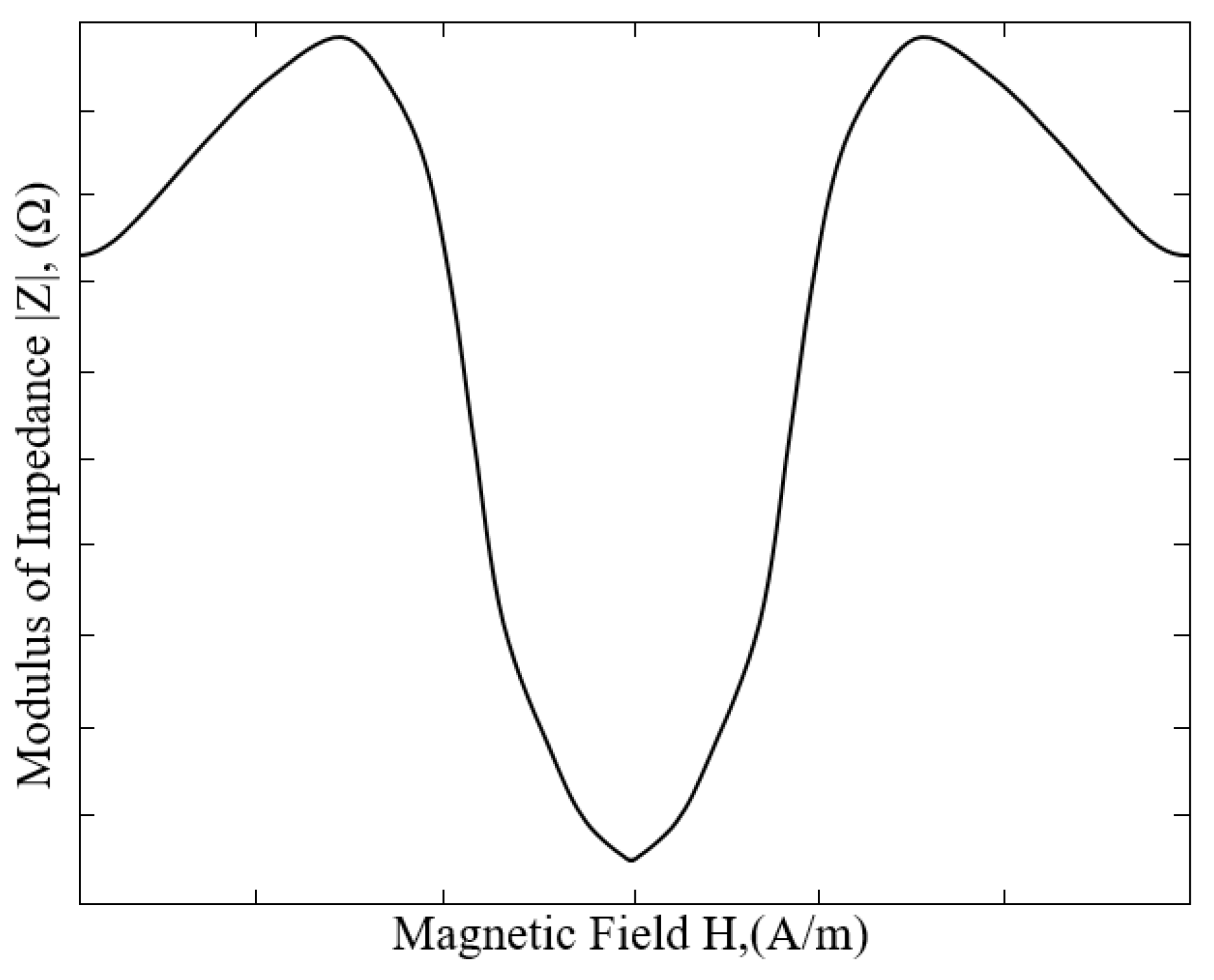
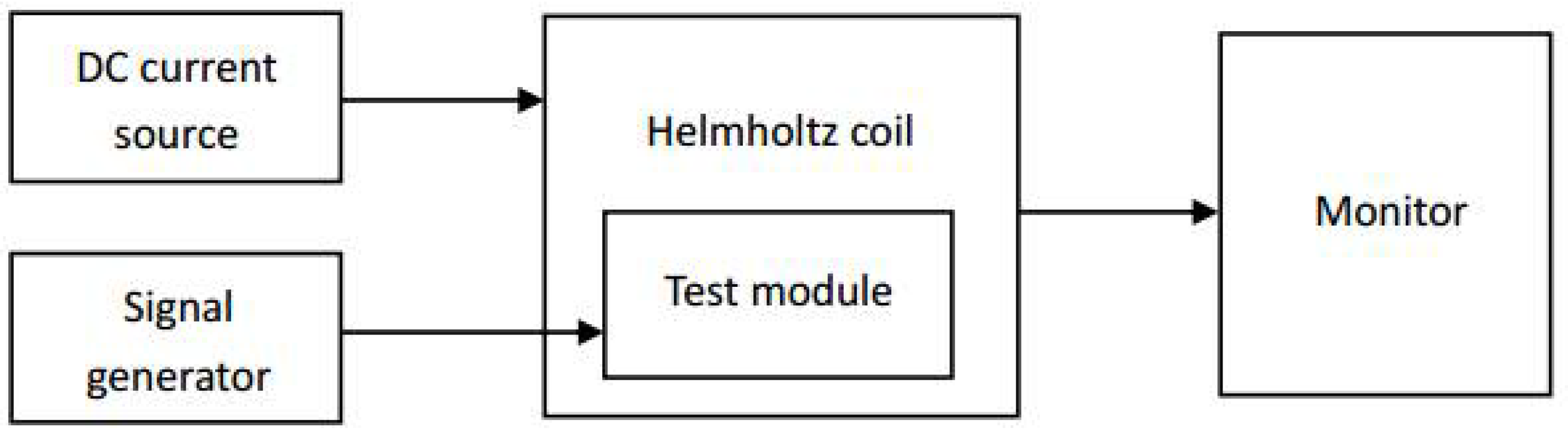
4.1. Passive Impedance Test
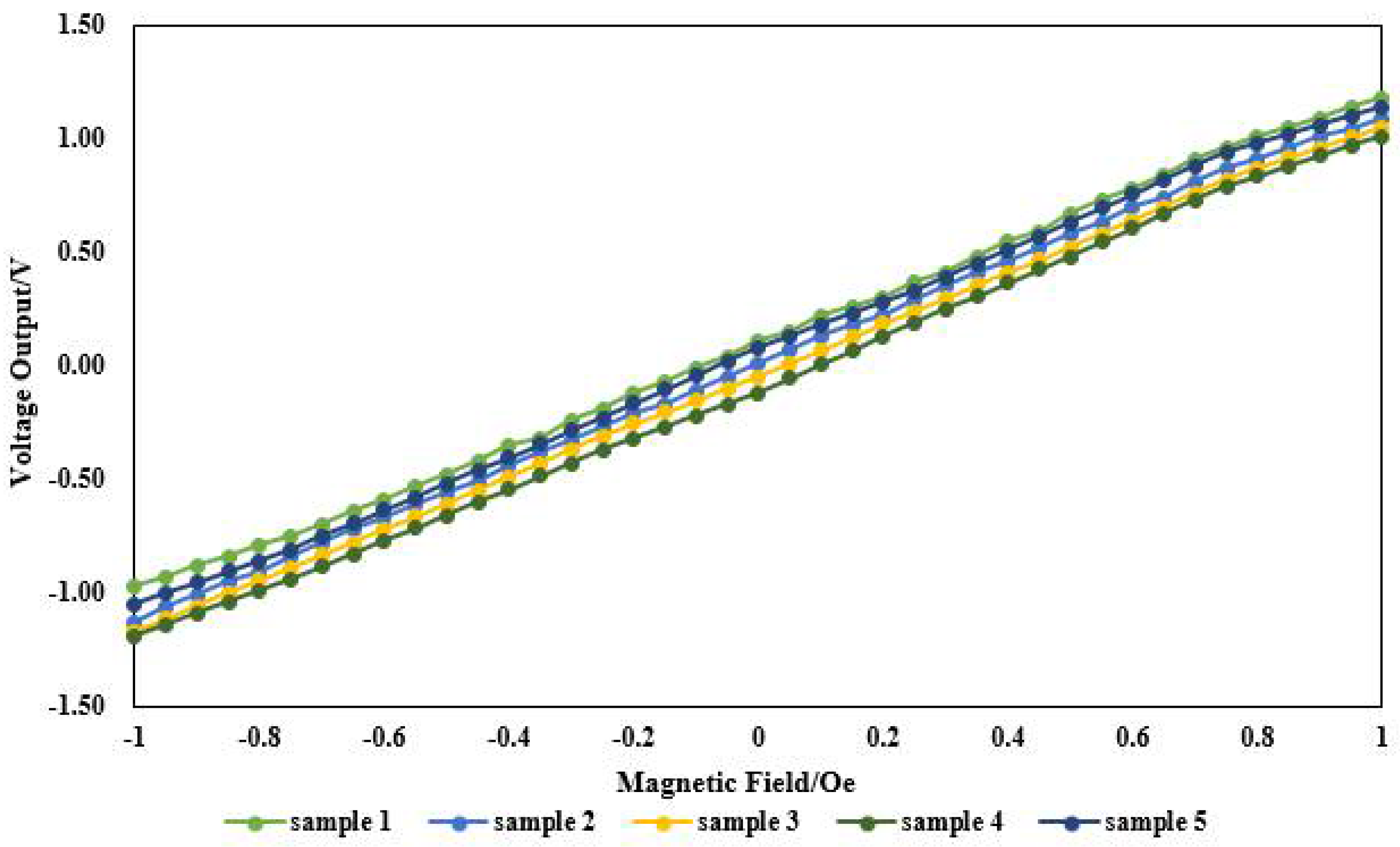
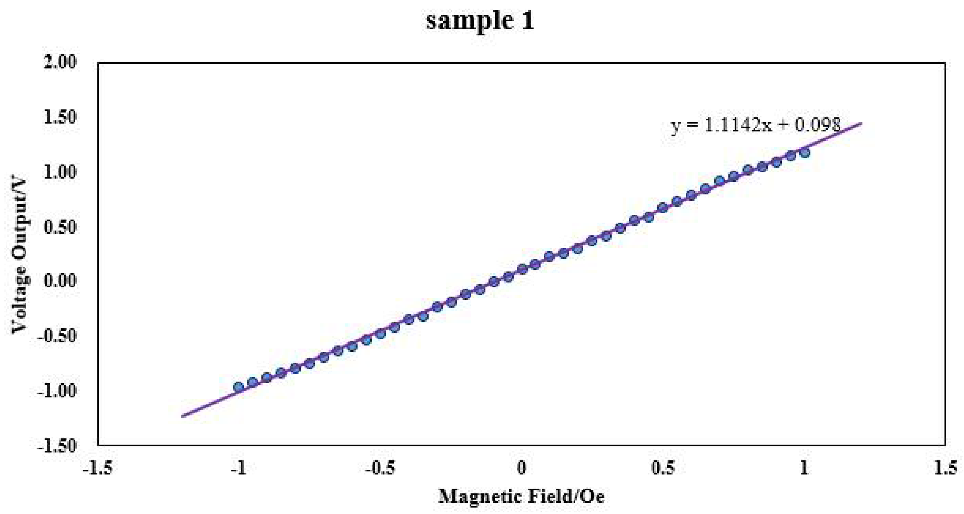
4.2. Active Impedance Test
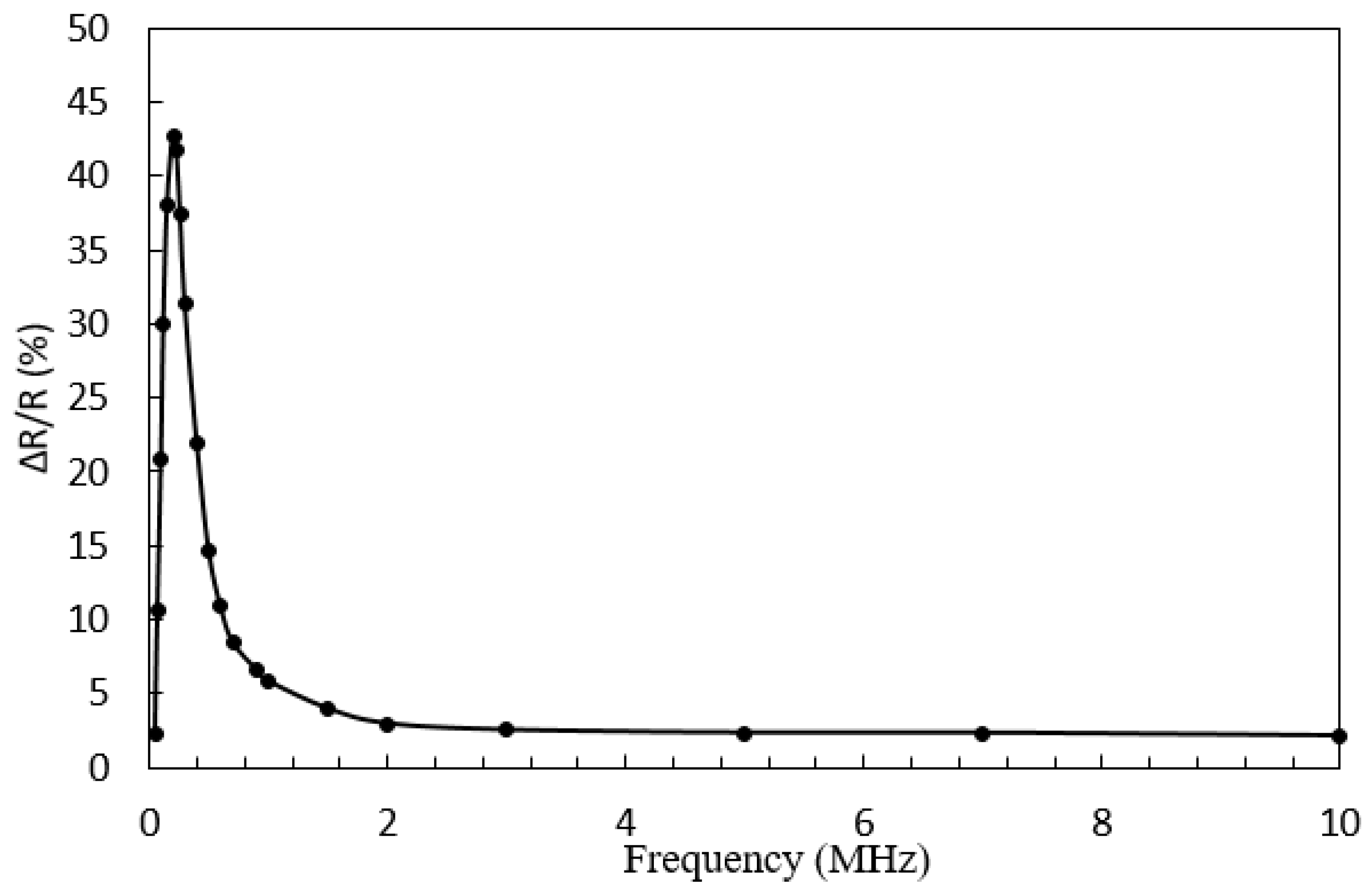
4.3. The Frequency Characteristic of Impedance
5. Conclusions
Author Contributions
Funding
Conflicts of Interest
References
- An, K.; Hu, J.; Zhang, L.; Qin, H.; Song, P. Giant Magnetoimpedance Analysis of Composite Amorphous alloy wire. Rare Met. Mater. Eng. 2005, 34, 1259–1262. [Google Scholar] [CrossRef]
- Panina, L.V.; Mohri, K.; Bushida, K.; Noda, M. Giant magnetoimpedance and magneto-inductive effects in amorphous alloys. J. Appl. Phys. 1994, 76, 6198–6203. [Google Scholar] [CrossRef]
- Zhang, L.; Pan, Z. Wavelet analysis of data from GMI magnetic sensors. J. Nat. Univ. Def. Technol. 2012, 34, 143–147. [Google Scholar] [CrossRef]
- Pan, Z.; Zhou, H.; Zhang, D.; Zhang, W. Advances in detection circuit of magnetic sensors based on giant magneto-impedance at abroad. Chin. J. Sci. Instrum. 2017, 38, 781–793. [Google Scholar]
- Honkura, Y. Development of amorphous alloy wire type MI sensors for automobile use. J. Magn. Magn. Mater. 2002, 249, 375–381. [Google Scholar] [CrossRef]
- Zhou, H.; Pan, Z.; Zhang, D. Operating Point Self-Regulator for Giant Magneto-Impedance Magnetic Sensor. Sensors 2017, 17, 1103. [Google Scholar] [CrossRef] [PubMed]
- Zhukov, A.; Ipatov, M.; Ahmed Talaat, A.; Blanco, J.M.; Churyukanova, M.; Zhukova, V. Studies of High-Frequency Giant Magnetoimpedance Effect in Co-Rich Amorphous Microwires. IEEE Trans. Magn. 2015, 51. [Google Scholar] [CrossRef]
- Liu, J.; Li, Z.; Shen, H.; Qin, F.; Jiang, S.; Du, Z.; Phan, M.-H.; Sun, J. Composite electroplating to enhance the GMI output stability of melt-extracted wires. Mater. Des. 2016, 96, 251–256. [Google Scholar] [CrossRef]
- NazariNejad, S.; Fomani, A.A.; Mansour, R. Giant Magneto-Impedance Thin Film Magnetic Sensor. IEEE Trans. Magn. 2013, 49, 3874–3877. [Google Scholar] [CrossRef]
- Chiriac, H.; Herea, D.D.; Corodeanu, S. Microwire array for giant magnetoimpedance detection of magnetic particles for biosensor prototype. J. Magn. Magn. Mater. 2007, 311, 425–428. [Google Scholar] [CrossRef]
- Blanc-Béguin, F.; Nabily, S.; Gieraltowski, J.; Turzo, A.; Querellou, S.; Salaun, P.Y. Cytotoxicity and GMI bio-sensor detection of maghemite nanoparticles internalized into cells. J. Magn. Magn. Mater. 2009, 321, 192–197. [Google Scholar] [CrossRef]
- Guo, L.; Zhi, S.; Sun, X.; Lei, C.; Zhou, Y. Ultrasensitive detection of bioanalytes based on signal amplification of coil-integrated giant magnetoimpedance biosystems. Sens. Actuators B 2017, 247, 1–10. [Google Scholar] [CrossRef]
- Colosimo, P.; Chen, A.; Devkota, J.; Srikanth, H.; Phan, M.H. Sensing RF and microwave energy with fiber Bragg grating heating via soft ferromagnetic glass-coated microwires. Sens. Actuators A 2014, 210, 25–31. [Google Scholar] [CrossRef]
- Chen, J.; Li, J.; Li, Y.; Chen, Y.; Xu, L. Design and Fabrication of a Miniaturized GMI Magnetic Sensor Based on Amorphous Wire by MEMS Technology. Sensors 2018, 18, 732. [Google Scholar] [CrossRef] [PubMed]
- Karnaushenko, D.; Karnaushenko, D.D.; Makarov, D.; Baunack, S.; Schäfer, R.; Oliver, G. Schmidt Self-Assembled On-Chip-Integrated Giant Magneto-Impedance Sensorics. Adv. Mater. 2015, 27, 6582–6589. [Google Scholar] [CrossRef] [PubMed]
- Jantaratana, P.; Sirisathitkul, C. Effects of thickness and heat treatments on giant magnetoimpedance of electrode posited cobalt on silver wires. IEEE Trans. Magn. 2006, 42, 358–362. [Google Scholar] [CrossRef]
- Kammouni, R.E.; Kurlyandskaya, G.V.; Vazquez, M.; Volchkov, S.O. Magnetic properties and magnetoimpedance of short CuBe/CoFeNi electroplated microtubes. Sens. Actuaors A Phys. 2016, 248, 155–161. [Google Scholar] [CrossRef]
- Nabias, J.; Asfour, A.; Yonnet, J.-P. The Impact of Bending Stress on the Performance of Giant Magneto-Impedance (GMI) Magnetic Sensors. Sensors 2017, 17, 640. [Google Scholar] [CrossRef] [PubMed]
- Mohri, K.; Panina, L.V.; Uchiyama, T.; Bushida, K.; Noda, M. Sensitive and quick response micro magnetic sensor utilizing magneto-impedance in Co-rich amorphous wires. IEEE Trans. Magn. 1995, 31, 1266–1275. [Google Scholar] [CrossRef]
- Yi, F.; Zhang, J.; Peng, L.; Han, Y. The Research of SU8 Resist UV Lithography. Micronanoelectr. Technol. 2003, 7, 126–128. [Google Scholar] [CrossRef]
- Phan, M.H.; Peng, H.X. Giant magnetoimpedance materials: Fundamentals and applications. Prog. Mater. Sci. 2008, 53, 323–420. [Google Scholar] [CrossRef]


| Name | Size | Sensitivity |
|---|---|---|
| GMI Thin Film Magnetic Sensor [9] | Meander Type Structures: 1 mm × 0.5 mm; Straight Wire Structures: the Length of Straight Wire is 10 mm | the Impedance in 200 kHz and 500 kHz is 136% and 145% |
| Coil-Integrated GMI Biosystems [10] | 7.5 mm × 6.5 mm | 3 ng/mL for Streptavidin-Coupled Dynabeads and 0.2 ng/mL for Alpha Fetoprotein (AFP) |
| Amorphous Wire Type MI Sensors for Automobile Use [5] | 4 mm × 3 mm × 2 mm | 250 mV/Oe |
| Soft Ferromagnetic Glass-Coated Microwires [11] | Wire Diameter is 14 µm, Wire Length is 3 cm | ~10 times at f = 3.25 GHz Relative to the Perturbation of the Microwave Field |
| Operating Point Self-Regulator for GMI Magnetic Sensor [6] | Wire Diameter is 30 µm, Wire Length is 10 mm, Solenoids Length is 50 mm | 0.0034 V/nT in the Range of 0–2 µT |
| Num | Resistance Value/Ω | Average Value/Ω | Deviation/Ω | Variance/Ω2 |
|---|---|---|---|---|
| 1 | 23.6 | 24.71 | 8.3 | 7.559 |
| 2 | 24.5 | |||
| 3 | 28.1 | |||
| 4 | 25.7 | |||
| 5 | 19.8 | |||
| 6 | 27.5 | |||
| 7 | 23.9 | |||
| 8 | 25.3 | |||
| 9 | 21.1 | |||
| 10 | 27.6 |
| Num | Resistance Value/Ω | Average Value/Ω | Deviation/Ω | Variance/Ω2 |
|---|---|---|---|---|
| 1 | 20.4 | 20.26 | 0.5 | 0.029 |
| 2 | 20.5 | |||
| 3 | 20.2 | |||
| 4 | 20.1 | |||
| 5 | 20.5 | |||
| 6 | 20.1 | |||
| 7 | 20.3 | |||
| 8 | 20.0 | |||
| 9 | 20.3 | |||
| 10 | 20.2 |
© 2018 by the authors. Licensee MDPI, Basel, Switzerland. This article is an open access article distributed under the terms and conditions of the Creative Commons Attribution (CC BY) license (http://creativecommons.org/licenses/by/4.0/).
Share and Cite
Chen, Y.; Li, J.; Chen, J.; Xu, L. Improving the Electrical Contact Performance for Amorphous Wire Magnetic Sensor by Employing MEMS Process. Micromachines 2018, 9, 299. https://doi.org/10.3390/mi9060299
Chen Y, Li J, Chen J, Xu L. Improving the Electrical Contact Performance for Amorphous Wire Magnetic Sensor by Employing MEMS Process. Micromachines. 2018; 9(6):299. https://doi.org/10.3390/mi9060299
Chicago/Turabian StyleChen, Yulong, Jianhua Li, Jianwen Chen, and Lixin Xu. 2018. "Improving the Electrical Contact Performance for Amorphous Wire Magnetic Sensor by Employing MEMS Process" Micromachines 9, no. 6: 299. https://doi.org/10.3390/mi9060299
APA StyleChen, Y., Li, J., Chen, J., & Xu, L. (2018). Improving the Electrical Contact Performance for Amorphous Wire Magnetic Sensor by Employing MEMS Process. Micromachines, 9(6), 299. https://doi.org/10.3390/mi9060299