Fabrication and Characteristics of SnAgCu Alloy Nanowires for Electrical Connection Application

1
Department of Industrial Education, National Taiwan Normal University, 106 Taipei, Taiwan
2
Department of Electron Microscopy Development Application, Industrial Technology Research Institute, 310 Hsinchu, Taiwan
3
Department of Mechanical Engineering, Lunghwa University of Science and Technology, 333 Taoyuan, Taiwan
*
Authors to whom correspondence should be addressed.
Micromachines 2018, 9(12), 644; https://doi.org/10.3390/mi9120644
Submission received: 15 November 2018
/
Revised: 27 November 2018
/
Accepted: 3 December 2018
/
Published: 5 December 2018
(This article belongs to the Special Issue New Perspectives in Nanowires: From Growth and Characterization to Technological Applications)
Abstract
:As electronic products become more functional, the devices are required to provide better performances and meet ever smaller form factor requirements. To achieve a higher I/O density within the smallest form factor package, applying nanotechniques to electronic packaging can be regarded as a possible approach in microelectronic technology. Sn-3.0 wt% Ag-0.5 wt% Cu (SAC305) is a common solder material of electrical connections in microelectronic devices. In this study, SAC305 alloy nanowire was fabricated in a porous alumina membrane with a pore diameter of 50 nm by the pressure casting method. The crystal structure and composition analyses of SAC305 nanowires show that the main structure of the nanowire is β-Sn, and the intermetallic compound, Ag3Sn, locates randomly but always appears on the top of the nanowire. Furthermore, differential scanning calorimetry (DSC) results indicate the melting point of SAC305 alloy nanowire is around 227.7 °C. The melting point of SAC305 alloy nanowire is significantly higher than that of SAC305 bulk alloy (219.4 °C). It is supposed that the non-uniform phase distribution and composite difference between the nanowires causes the change of melting temperature.
1. Introduction
Electronic packaging is the final manufacturing process to transform semiconductor devices into functional products and advanced packaging has a direct impact on product performance and success rates [1,2]. As electronic and mobile devices continue to develop, the devices are required to meet the demand of ultra-thin, ultra-light, high performance, and low power consumption. Therefore, advanced 3D microelectronic packaging technology is becoming the industry trend [3,4,5,6]. More and more Input/Output (I/O) pins are needed in electronic packaging of integrated circuits while pitch is getting smaller and smaller. In order to achieve fine pitch requirement, applying nanotechniques to electronic packaging can be regarded as a possible approach in microelectronic technology. In recent years, nano-sized interconnections for advanced packaging have drawn much attention from researchers and scientists. Nanosolder is necessary to performed the soldering or bonding at the nanoscale.
Among the numerous solder materials, tin-silver-copper (SAC) based alloys are widely used to replace the conventional tin-lead solders and have advantages such as low melting temperature, superior mechanical properties, and good solderability [7,8]. Nanoscale SAC solder alloys [9,10,11,12,13,14,15,16] such as nanoparticles and nanowires had been prepared in these years. SAC alloy nanoparticles could be produced by chemical methods and physical methods, such as electrodeposition, chemical reduction technique, consumable-electrode direct current arc technique, etc. These nanoparticles were easy to aggregate yet difficult to handle and perform soldering directly. SAC alloy nanowires such as Sn88Ag5Cu7, Sn93Ag4Cu3, Sn58Ag18Cu24, Sn78Ag16Cu6, Sn90Ag4Cu6, Sn87Ag4Cu9 alloy nanowires were fabricated by electrodeposition using various values of the deposition potential [16]. However, SAC305 alloy, a common commercial lead-free solder alloy, has not been produced in the form of nanowire until now.
In this study, we fabricated SAC305 alloy nanowires inside the porous alumina membrane by the pressure casting method. The structural and thermal characteristics of SAC305 alloy nanowires were investigated and the differences from SAC305 bulk alloy were studied. Furthermore, the nanowire array in the soldering application was also discussed in this work.
2. Materials and Methods
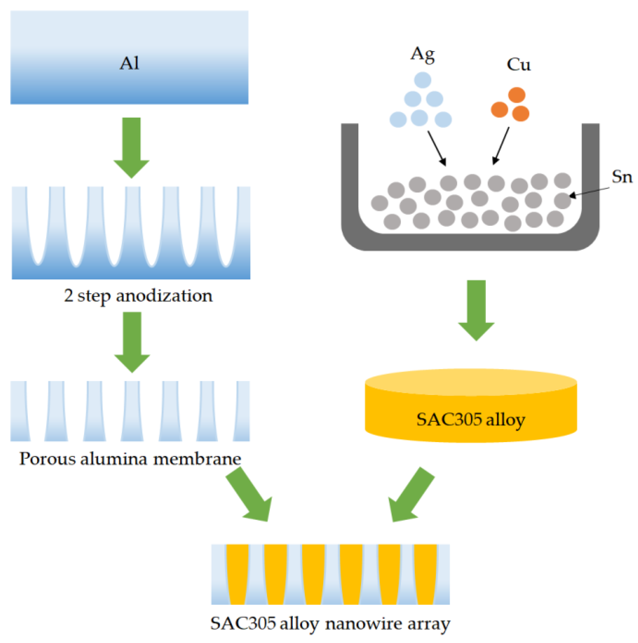
Solder alloy nanowire array was fabricated in a porous alumina membrane with a pore diameter around 50 nm by the pressure casting method. The processes were divided into three parts: production of the porous alumina template, smelting of the solder alloy, and fabrication of the alloy nanowires. The detail process flow is shown in Figure 1. Firstly, the porous alumina template was fabricated using a two-step anodization. An Al sheet (purity 99.7%) was anodized in 0.3 M oxalic acid solution (H2C2O4) at 20 °C for 1 h. Then, the alumina film formed by the first anodization was removed in a solution, which was composed of the phosphoric acid (H3PO4) and the chromic acid (H2CrO4) at 60 oC. The second anodization was performed using the condition of the first anodization. After removing the Al substrate and the barrier layer by 0.1 M sodium hydroxide solution (NaOH), the porous alumina membrane was produced.
Secondly, pure tin (Sn) particles (purity 99.99%), pure silver (Ag) particles (purity 99.99%), and pure cupper (Cu) particles (purity 99.99%) were well mixed in a quartz crucible. The weights of the three pure metals (Sn, Ag, and Cu) were in the ratio of 96.5:3.0:0.5. After that, the quartz crucible was heated to 1100 °C in vacuum. The alloy, Sn-3.0 wt% Ag-0.5 wt% Cu (SAC305), was formed after cooling to room temperature.
Finally, SAC305 alloy nanowire array was produced using the high vacuum pressure casting technique. The experimental equipment and principle were described in detail in our previous studies [17,18]. The porous alumina membrane produced in this work had a thickness of 10 μm and the area of the membrane was 1cm2. A disc shaped piece of SAC305 alloy with dimensions of 1 cm2 × 0.1 cm was placed on the top of the porous alumina membrane inside the chamber. The vacuum pressure of the chamber was maintained at 10−6 Torr to prevent the metal oxidation. After the chamber was heating to 300 °C for 20 min, a hydraulic force was applied to SAC305 alloy melt. During casting process, the molten alloy was injected into the nanochannel of the porous alumina membrane. Solidification was performed using water quenching at the bottom of the chamber. After cooling to room temperature, SAC305 alloy nanowire array was produced.
The crystal structure, phase distribution, and composition of SAC305 alloy nanowires were examined by X-ray diffraction (XRD, Bruker, Billerica, MA, USA) scanning electron microscope (SEM, JEOL, Tokyo, Japan), energy dispersive spectroscopy (EDS, Oxford, Abingdon, UK), and transmission electron microscope (TEM, JEOL, Tokyo, Japan). Moreover, the melting point and thermal properties of SAC305 alloy nanowires were measured by differential scanning calorimetry (DSC, TA, New Castle, DE, USA) analysis.
3. Results and Discussion
3.1. Fabrication of SAC305 Alloy Nanowires
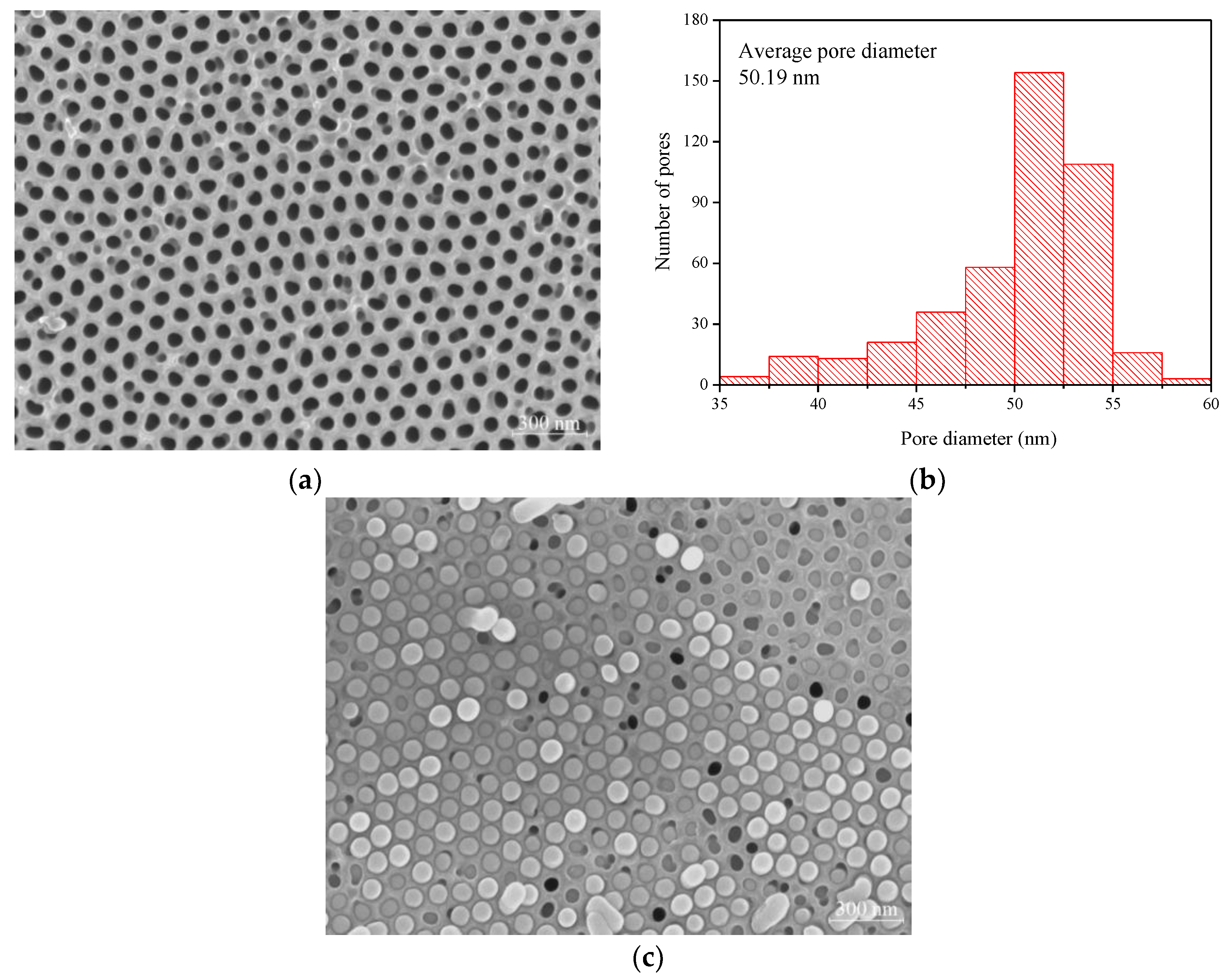
In this study, SAC305 nanowires were fabricated in the porous alumina membrane by the pressure casting process. Figure 2a shows that the surface morphology of the porous alumina membrane produced in the oxalic acid solution reveals that the nanopores are order and uniform arrays. The SEM image of the porous alumina membrane is further analyzed with the image pro plus software. The corresponding pore size distribution was obtained by the histogram analysis. As presented in Figure 2b, the histogram was plotted by measuring at least 400 pores in Figure 2a and the average pore diameter is about 50.19 nm. Figure 2c shows the plane view of SAC305 alloy nanowires in the porous alumina membrane. A high filling ratio of nanowire could be achieved by the pressure casting process.
3.2. Characteristics of SAC305 Alloy Nanowires
X-ray diffraction analyses of SAC305 bulk alloy and nanowires are shown in Figure 3. The signals of Sn in SAC305 bulk alloy and nanowires are identified as beta-Sn (β-Sn). The β-Sn phase crystallizes in a tetragonal crystal structure (I41/and, space group = 141, JCPDS No. 04-0673) with the lattice constants, a = 0.5831 nm and c = 0.3182 nm. The major crystal plane of β-Sn in SAC305 bulk alloy and nanowires is the (200) lattice plane locating at the angle of 30.6°. Some slight signals form Ag3Sn are also observed. The results indicate that the crystal structure of SAC305 bulk alloy is preserved in the nanowires after heating and high-pressure processes. Additionally, the diffraction peak of Al in SAC305 alloy nanowires is coming from the residual Al substrate of the porous alumina membrane.
The low-magnification cross-sectional structure of SAC305 alloy nanowires is presented in the bright field TEM image as shown in Figure 4a. Figure 4b, which is the enlarged image of the red box in Figure 4a, reveals a significant contrast difference and interface in the upper region of the nanowire. EDS analysis was performed with field emission TEM to determine the composition of nanowire marked in Figure 4b. From the EDS spectrum, the crystal on the top of the nanowire (area a) is judged to consist of Ag and Sn in the ratio of 3:1 with a statistical error of 5%. The gold signal is coming from the TEM gold grid. Area b is mainly composed of Sn, but a low Cu content around 0.5 wt% is also observed. High-resolution TEM analyses were performed to determine the crystal structure of the nanowire. Figure 5b is taken from the top of the nanowire. It indicates that the lattice fringes (d = 2.59 Å) observed in the high-resolution TEM image is identical with the distance between the (201) lattice plane and confirms that the nanocrystal is Ag3Sn. The high-resolution TEM (Figure 5c) of the region under the Ag3Sn crystal in the nanowire shows that the lattice fringes, d = 2.92 Å and d = 2.79 Å, are identical to the distance between the (200) lattice plane and (101) lattice plane of β-Sn, respectively. Fast Fourier-Transformation (FFT) analysis was performed on the lattice fringes of Figure 5c and the spots with a zone axis [10] match well with the tetragonal structure of β-Sn as shown in Figure 5d. According to the TEM and EDS results, the nanowire is mainly composed of β-Sn. Furthermore, a Ag3Sn crystal always appears on the top of the nanowire and has a non-uniform distribution in the nanowire arrays. However, the intermetallic compounds composed of Sn and Cu such as Cu6Sn5 and Cu3Sn were not found in our experiment. It is supposed that the reason for this is that Cu6Sn5 or Cu3Sn has a smaller crystal size and much lower content than Ag3Sn, causing difficulty in observation.
The DSC curves in Figure 6 show that there is a variation in the melting point between SAC305 bulk alloy and the nanowires. The melting temperature increases from 219.4 °C to 227.7 °C as the alloy’s crystal size decreases. For nanocrystals embedded in a matrix, they can melt below the melting point of the bulk materials when the interfaces between embedded nanocrystals and the matrix are incoherent [19]. Moreover, the melting point depends strongly on the surface to volume ratio in the nanoscale range [20]. Our experimental result does not agree with the theoretical prediction but is just the reverse. This could be explained by the fact that not only the crystal size decreases but also the composition and phase distribution change during the formation of the nanowire. TEM and EDS results indicate that the intermetallic compound, Ag3Sn, always appears on the top of the nanowires and the composition of the nanowire except Ag3Sn crystal is mainly composed of Sn and Cu (~0.5 wt%). According to the Sn–Ag–Cu ternary phase diagram [21], the melting point of SAC 305 alloy is around 220 °C and the melting point of SAC alloy increases as the decrease of Ag content. Furthermore, Ag diffusion during the heating process might become difficult because of the confinement of the nanochannel in the porous alumina membrane. Therefore, the melting behavior of SAC305 alloy nanowire is more similar to the Sn–Cu system rather than the Sn–Ag–Cu system, leading to the higher melting point than SAC305 bulk alloy.
Fine pitch and submicron bump technology is a possible way to achieve a higher I/O density within the smallest form factor package. In this study, we propose a new joint structure with the solder alloy nanowire array as shown in Figure 7 for the submicron electronic packaging. The solder alloy nanowires are the bridges between the solder cap on the Cu pillar and the pre-solder of the substrate or another chip. Some advantages such as offering more overlay budget and reducing the common soldering problems like cold joints and solder bridges could be obtained using the new joint structure. Although there are still concerns about reliability and mechanical stress issues, this technique could be helpful to develop the interconnection technology for the advanced packaging where high-density joint interconnection is required. Additionally, more stable and more flexible nanostructured templates with the suitable coefficient of thermal expansion (CTE) would be a good candidate reducing the joint stress for the practical application [22,23].
4. Conclusions
SAC305 alloy nanowires have been successfully fabricated inside the porous alumina membrane by the pressure casting method. The nanowires with high aspect ratio are arranged uniformly. Experimental results show that the intermetallic compound, Ag3Sn, locates randomly but always appears on the top of the nanowire. The composition of the nanowire, except Ag3Sn crystal, is mainly composed of Sn and Cu (~0.5 wt%). DSC results indicate that SAC305 alloy nanowire has a higher melting temperature than SAC305 bulk alloy. The melting point increase from 219.4 °C to 227.7 °C might be caused by the non-uniform phase distribution and composition difference. Finally, we propose a possible joint structure in which the solder alloy nanowires could provide an electrical connection between chip and substrate or chip and chip to achieve the high-density joint interconnection.
Author Contributions
J.-H.C. and C.-Y.H. conceived and designed the experiments; J.-H.C. performed the experiments; S.-C.L. and S.-C.H. analyzed the data; S.-C.L. contributed analysis tools; J.-H.C. wrote the paper.
Acknowledgments
The authors gratefully acknowledge the support of the Ministry of Science and Technology of the Republic of China, through Grant No. MOST106-2218-E-003-002.
Conflicts of Interest
The authors declare no conflicts of interest.
References
- Yoon, S.W.; Petrov, B.; Liu, K. Advanced wafer level technology: Enabling innovations in mobile, IoT and wearable electronics. In Proceedings of the Electronics Packaging and Technology Conference (EPTC), Singapore, 2–4 December 2015. [Google Scholar]
- Lau, J.H. Evolution, challenge, and outlook of TSV, 3D IC integration and 3D silicon integration. In Proceedings of the Advanced Packaging Materials (APM), Xiamen, China, 25–28 October 2011. [Google Scholar]
- Lancaster, A.; Keswani, M. Integrated circuit packaging review with an emphasis on 3D packaging. Integration 2018, 60, 204. [Google Scholar] [CrossRef]
- Tu, K.N. Reliability challenges in 3D IC packaging technology. Microelectron. Reliab. 2011, 51, 517. [Google Scholar] [CrossRef]
- Liu, Y.; Chu, Y.C.; Tu, K.N. Scaling effect of interfacial reaction on intermetallic compound formation in Sn/Cu pillar down to 1 μm diameter. Acta Mater. 2016, 117, 146. [Google Scholar] [CrossRef]
- Tu, K.N.; Tian, T. Metallurgical challenges in microelectronic 3D IC packaging technology for future consumer electronic products. Sci. China Technol. Sci. 2013, 56, 1740. [Google Scholar] [CrossRef]
- Gao, L.; Xue, S.; Zhang, L.; Sheng, Z.; Ji, F.; Dai, W.; Yu, S.L.; Zeng, G. Effect of alloying elements on properties and microstructures of SnAgCu solders. Microelectron. Eng. 2010, 87, 2025. [Google Scholar] [CrossRef]
- Xiao, H.; Chan, Y.C.; Zhu, Z.; Wu, F. Investigation in microstructure and mechanical properties of Ni-coated multi-wall carbon nanotubes doped Sn3.0Ag0.5Cu solder alloys. In Proceedings of the Electronic System-Integration Technology Conference (ESTC), Grenoble, France, 3–15 September 2016. [Google Scholar]
- Delsante, S.; Novakovic, R.; Borzone, G. Synthesis, characterization and thermal stability of SnAg and SnAgCu nanoparticles. J. Alloy. Compd. 2018, 747, 385. [Google Scholar] [CrossRef]
- Foo, S.P.; Siow, K.S.; Jalar, A. Synthesizing SnAgCu nanoparticles by electrodeposition of reverse microemulsion electrolyte. In Proceedings of the Semiconductor Electronics (ICSE), Kuala Lumpur, Malaysia, 27–29 August 2014. [Google Scholar]
- Wang, Y.; Liu, W.; Liu, W.; He, P.; Fan, Z.; Wang, X.; Yu, D.; Guo, J.; Guo, B.; Shen, H. Synthesis of SnAgCu nanoparticles with low melting point by the chemical reduction method. Microelectron. Reliab. 2017, 78, 17. [Google Scholar] [CrossRef]
- Roshanghias, A.; Yakymovych, A.; Bernardi, J.; Ipser, H. Synthesis and thermal behavior of tin-based alloy (Sn–Ag–Cu) nanoparticles. Nanoscale 2015, 7, 5843. [Google Scholar] [CrossRef] [PubMed]
- Roshanghias, A.; Vrestal, J.; Yakymovych, A.; Richter, K.W.; Ipser, H. Sn–Ag–Cu nanosolders: Melting behavior and phase diagram prediction in the Sn-rich corner of the ternary system. Calphad 2015, 49, 101. [Google Scholar] [CrossRef] [PubMed]
- Hsiao, L.Y.; Duh, J.G. Synthesis and characterization of lead-free solders with Sn-3.5 Ag-xCu (x = 0.2, 0.5, 1.0) alloy nanoparticles by the chemical reduction method. J. Electrochem. Soc. 2005, 152, J105. [Google Scholar] [CrossRef]
- Gao, Y.; Zou, C.; Yang, B.; Zhai, Q.; Liu, J.; Zhuravlev, E.; Schick, C. Nanoparticles of SnAgCu lead-free solder alloy with an equivalent melting temperature of SnPb solder alloy. J. Alloy. Compd. 2009, 484, 777. [Google Scholar] [CrossRef]
- Atalay, F.E.; Avsar, D.; Kaya, H.; Yagmur, V.; Atalay, S.; Seckin, T. Nanowires of lead-free solder alloy SnCuAg. J. Nanomater. 2011, 2011, 37. [Google Scholar] [CrossRef]
- Chen, J.H.; Lo, S.C.; Chao, C.G.; Liu, T.F. Microstructure and properties of Pb nanowires fabricated by casting. Jpn. J. Appl. Phys. 2008, 47, 4815. [Google Scholar] [CrossRef]
- Kuo, C.G.; Chen, J.H.; Liu, Y.H. Fabrication of a zinc aluminum oxide nanowire array photoelectrode for a solar cell using a high vacuum die casting technique. Int. J. Photoenergy 2014, 2014, 302075. [Google Scholar] [CrossRef] [PubMed]
- Zhang, Z.; Li, J.C.; Jiang, Q. Modelling for size-dependent and dimension-dependent melting of nanocrystals. J. Phys. D: Appl. Phys. 2000, 33, 2653. [Google Scholar] [CrossRef]
- Abdullah, B.J.; Omar, M.S.; Jiang, Q. Size dependence of the bulk modulus of Si nanocrystals. Sādhanā 2018, 43, 174. [Google Scholar] [CrossRef]
- Kattner, U.R. Phase diagrams for lead-free solder alloys. Jom 2002, 54, 45. [Google Scholar] [CrossRef]
- Aramesh, M.; Mayamei, Y.; Wolff, A.; Ostrikov, K.K. Superplastic nanoscale pore shaping by ion irradiation. Nat. Commun. 2018, 9, 835. [Google Scholar] [CrossRef] [PubMed]
- Aramesh, M.; Djalalian-Assl, A.; Aghili Yajadda, M.M.; Prawer, S.; Ostrikov, K. Thin nanoporous metal–insulator–metal membranes. ACS Appl. Mater. Interfaces 2016, 8, 4292. [Google Scholar] [CrossRef] [PubMed]
Figure 1.
Schematic process flow of SAC305 alloy nanowires fabrication in this study.

Figure 2.
(a) SEM image of the porous alumina membrane; (b) The pore size distribution which was calculated from image (a) and the average pore diameter denoted in the figure; (c) SEM image of SAC305 alloy nanowires in the porous alumina membrane.
Figure 2.
(a) SEM image of the porous alumina membrane; (b) The pore size distribution which was calculated from image (a) and the average pore diameter denoted in the figure; (c) SEM image of SAC305 alloy nanowires in the porous alumina membrane.

Figure 3.
XRD spectra of SAC305 alloy and SAC305 alloy nanowires.

Figure 4.
(a) Low magnification TEM image of SAC305 alloy nanowires; (b) The enlarged image of the red square in the image (a); (c) Energy dispersive X-ray spectra recorded from the circular areas in (b).
Figure 4.
(a) Low magnification TEM image of SAC305 alloy nanowires; (b) The enlarged image of the red square in the image (a); (c) Energy dispersive X-ray spectra recorded from the circular areas in (b).

Figure 5.
(a) TEM image of the interface between Ag3Sn and β-Sn. (b) High-resolution TEM image of Ag3Sn crystal. (c) High-resolution TEM image of β-Sn crystal. (d) FFT analysis of the lattice fringes in (c).
Figure 5.
(a) TEM image of the interface between Ag3Sn and β-Sn. (b) High-resolution TEM image of Ag3Sn crystal. (c) High-resolution TEM image of β-Sn crystal. (d) FFT analysis of the lattice fringes in (c).


Figure 6.
Differential scanning calorimetry (DSC) thermographs of SAC305 alloy and SAC305 alloy nanowires.
Figure 6.
Differential scanning calorimetry (DSC) thermographs of SAC305 alloy and SAC305 alloy nanowires.

Figure 7.
Schematic illustration of an electrical connection structure with the solder alloy nanowires.
Figure 7.
Schematic illustration of an electrical connection structure with the solder alloy nanowires.

© 2018 by the authors. Licensee MDPI, Basel, Switzerland. This article is an open access article distributed under the terms and conditions of the Creative Commons Attribution (CC BY) license (http://creativecommons.org/licenses/by/4.0/).
Share and Cite
MDPI and ACS Style
Chen, J.-H.; Lo, S.-C.; Hsu, S.-C.; Hsu, C.-Y. Fabrication and Characteristics of SnAgCu Alloy Nanowires for Electrical Connection Application. Micromachines 2018, 9, 644. https://doi.org/10.3390/mi9120644
AMA Style
Chen J-H, Lo S-C, Hsu S-C, Hsu C-Y. Fabrication and Characteristics of SnAgCu Alloy Nanowires for Electrical Connection Application. Micromachines. 2018; 9(12):644. https://doi.org/10.3390/mi9120644
Chicago/Turabian StyleChen, Jung-Hsuan, Shen-Chuan Lo, Shu-Chi Hsu, and Chun-Yao Hsu. 2018. "Fabrication and Characteristics of SnAgCu Alloy Nanowires for Electrical Connection Application" Micromachines 9, no. 12: 644. https://doi.org/10.3390/mi9120644
Note that from the first issue of 2016, this journal uses article numbers instead of page numbers. See further details here.