
Two-Dimensional Magnetic Field Sensor Based on Silicon Magnetic Sensitive Transistors with Differential Structure

Key Laboratory of Electronics Engineering, College of Heilongjiang Province, Heilongjiang University, Harbin 150080, China
*
Author to whom correspondence should be addressed.
Micromachines 2017, 8(4), 95; https://doi.org/10.3390/mi8040095
Submission received: 10 December 2016
/
Revised: 16 February 2017
/
Accepted: 17 March 2017
/
Published: 23 March 2017
Abstract
:A two-dimensional (2D) magnetic field sensor consisting of four silicon magnetic sensitive transistors (SMSTs) with similar characteristics is presented in this paper. By use of micro-electromechanical systems (MEMS) and integrated packaging technology, this sensor fabricated by using the silicon wafer with a <100> orientation and high resistivity, was packaged on printed circuit boards (PCBs). In order to detect the magnetic fields in the x and y axes directions, two of the four SMSTs with opposite magnetic sensitive directions were located along the x and −x axes directions, symmetrically, and the others were located along the y and −y axes directions. The experimental results show that when the VCE = 10.0 V and IB = 6.0 mA, the magnetic sensitivities of the sensor in the x and y axes directions are 366.0 mV/T and 365.0 mV/T, respectively. It is possible to measure the 2D magnetic field and improve the magnetic sensitivity, significantly.
1. Introduction
To the best of our knowledge, with the development of complementary metal-oxide-semiconductor (CMOS) and micro-electromechanical systems (MEMS) technology, magnetic field sensors have been applied in many different fields, such as in the detection of the Earth’s magnetic field and angular position, etc. [1,2,3]. To date, the widely used magnetic sensitivity sensors include Hall sensor, giant magnetoresistance (GMR), magnetic sensitive transistor, and so on [4,5,6]. In 2003, the silicon magnetic sensitive transistor (SMST) with a cubic structure was fabricated by MEMS technology [7,8], achieving a maximum relative magnetic sensitivity of about 22.7%/kG. In 2013, the SMSTs with a differential structure were fabricated by MEMS technology and achieved an absolute magnetic sensitivity of 102.9 mV/kG [9]. In 2015, a two-dimensional (2D) magnetic field sensor based on the operating principle and characteristics of the magnetic sensitive diode (MSD) was proposed [10], exhibiting sensitivities of SxB = 544 mV/T and SyB = 498 mV/T in the x and y directions, respectively. In 2010, in order to improve the efficiency of the magnetic modulating system, a 2D Hall micro-sensor with lower noise and angular positioning function was proposed [11]. In 2013, based on peripheral processing electronics, a new type of 2D differential folded CMOS Hall device with higher accuracy was devised by integrating magneto-transistors in a single chip and connecting a p-substrate to the minimum power supply [12], so as to obviously reduce noise and cross-sensitivity.
In view of the operating principle and characteristics of the SMST, a 2D magnetic field sensor composed of two differential structures with four SMSTs is proposed in this paper. The sensor was studied by using a magnetic field generator system. The detection of two-dimensional magnetic fields is significantly enhanced by using the differential structures and a referable uniform magnetic sensitivity is realized.
2. Basic Structure and Operation Principle
2.1. Basic Structure
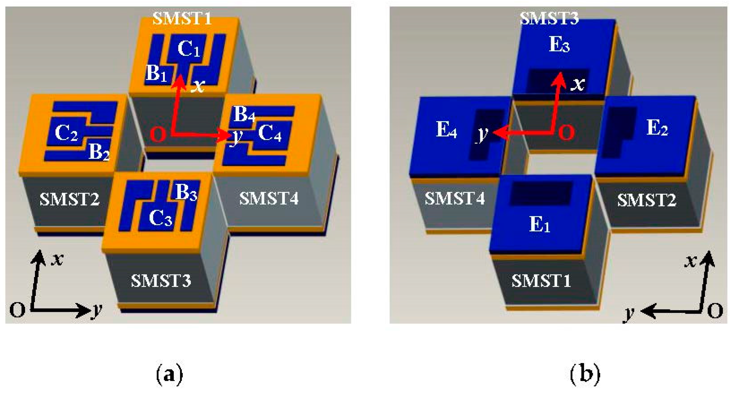
Figure 1 shows the cubic structure of the SMST based on MEMS technology. It has a C-type silicon cup, an emitter (E), a base (B) and a collector (C); the C and B are on top of E. The thickness d of the C-type silicon cup diaphragm is 30 µm, and the width W and the length L of the base region of the SMST are 30 µm and 120 µm, respectively. The cross-section area of the chip is 2000 μm × 2000 μm. As shown in Figure 2, the 2D magnetic field sensor is made up of two differential structures consisting of the four SMSTs with opposite magnetic sensitive directions, where one of the differential structures is constructed by SMST1 and SMST3 located along the x and −x axes, and another is composed of the SMST2 and SMST4 along the y and −y axes. The sensor has a common emitter E, four collectors (C1, C2, C3, C4), and four bases (B1, B2, B3, B4).
2.2. Operation Principle
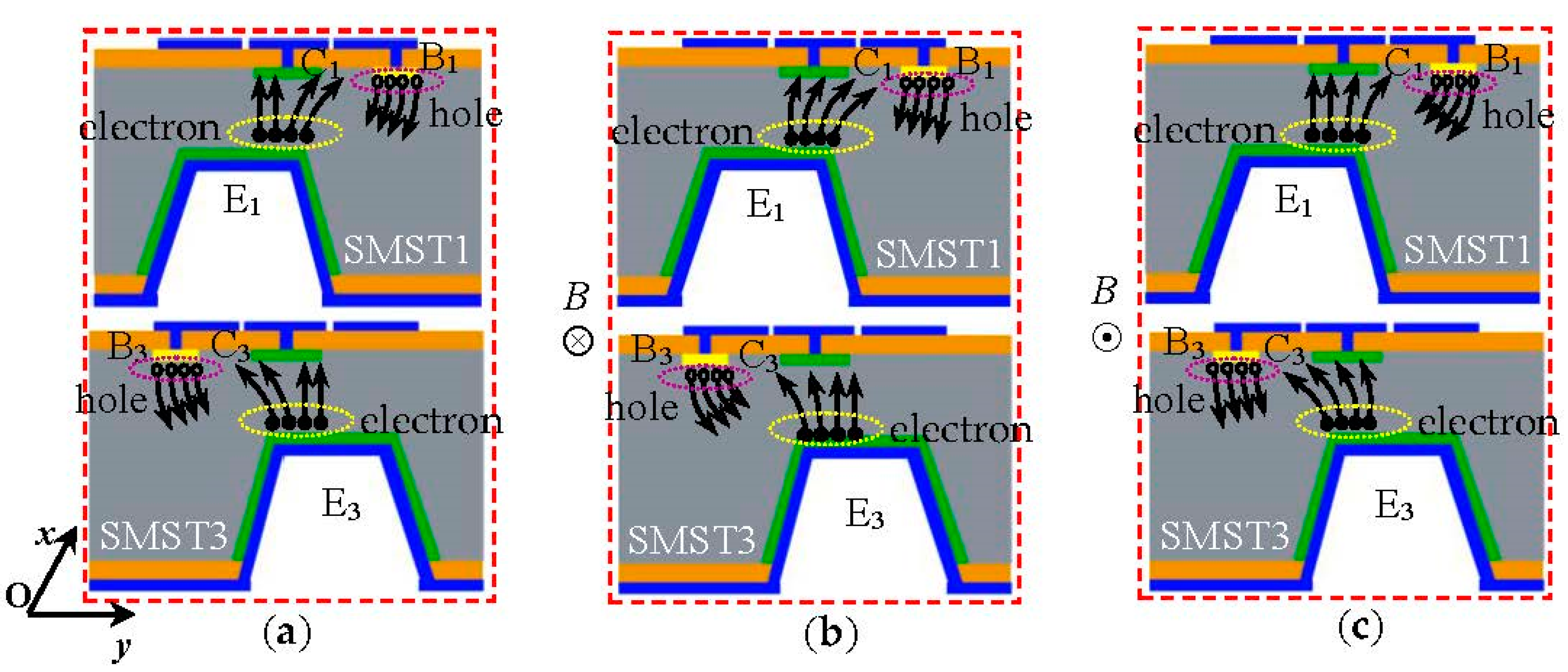
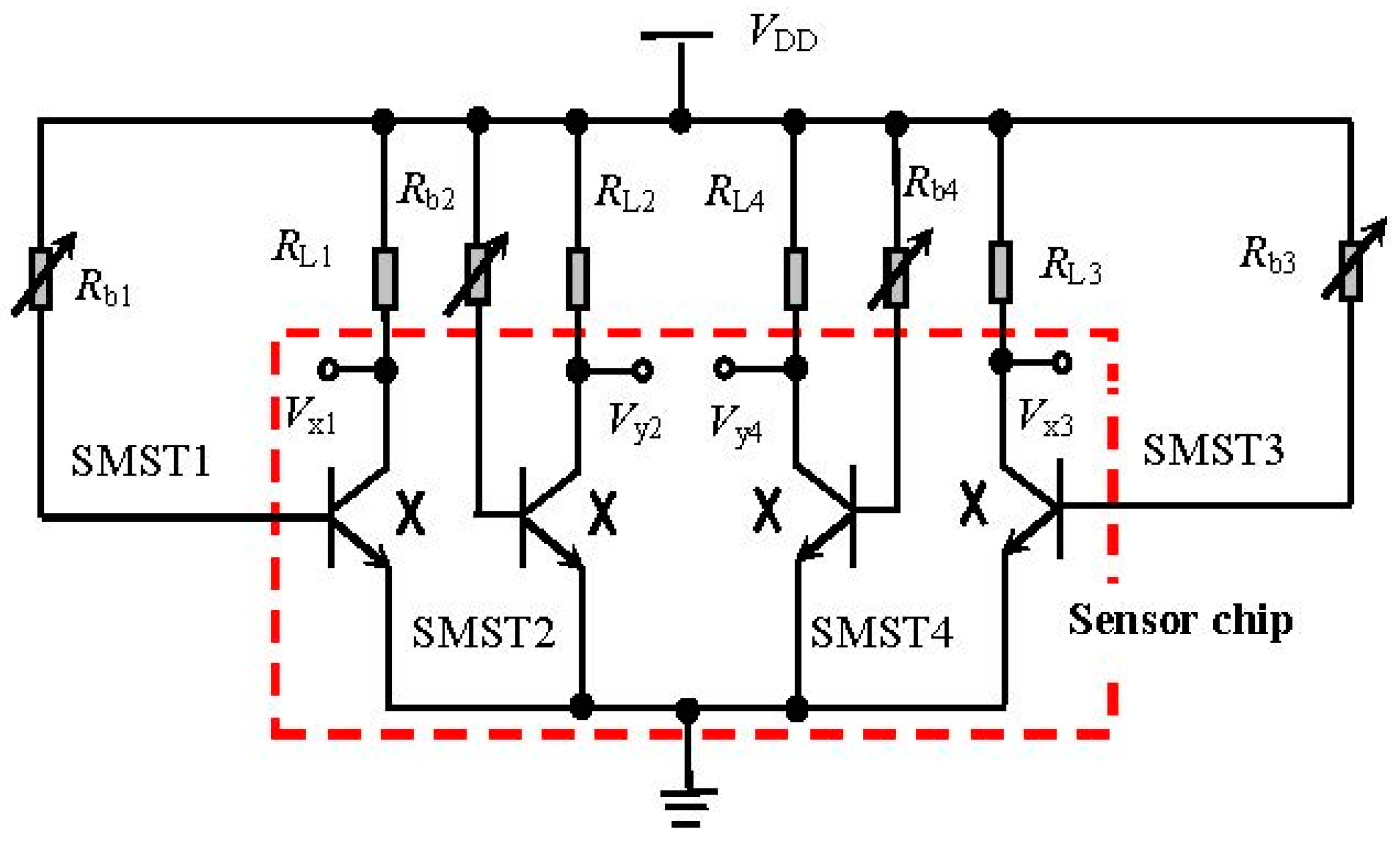
Figure 3a–c shows the cross-section views of the SMST1 and SMST3 along opposite magnetic sensitive directions; the operation principle for the 2D magnetic field sensor is discussed on the basis of the carriers deflected by different external magnetic fields. Figure 4 shows the test equivalent circuit of the 2D magnetic field sensor, where Vx1, Vy2, Vx3 and Vy4 are the collector voltages for the SMST1, SMST2, SMST3, and SMST4; RL1, RL2, RL3 and RL4 are the collector load resistances placed between the supply voltage VDD and the collectors C1, C2, C3 and C4, respectively. Rb1, Rb2, Rb3 and Rb4 are the base resistances placed between the supply voltage VDD and the bases B1, B2, B3 and B4, respectively. The four integrated packaging SMSTs are given in the dashed square, as shown in Figure 4.
In the ideal case, the two SMSTs along the x axis have the same characteristics, in which the deflection of carriers is the same under no external magnetic field, as shown in Figure 3a. The collector output voltage Vx along the x axis is:
where the collector current IC01 of the SMST1 is equal to the collector current IC03 of the SMST3.
Vx = Vx1 − Vx3 = IC03·RL3 − IC01·RL1 = 0
In contrast, when exerting an external magnetic field B parallel to the chip that is along the x and −x axes respectively, the carriers would be deflected by the Lorentz force as shown in Figure 3b,c. When the magnetic field direction in Figure 3b is defined as positive (B > 0 T); the carriers of SMST1 are deflected to a recombination region, as a sequence; IC1 is decreased and its decrement is ΔIC1; the collector IC3 of the SMST3 is increased and its increment is ΔIC3; the output voltage Vx can be obtained:
where the values of ΔVx1 and ΔVx3 are the variables of collector output voltages for the SMST1 and SMST3 under the external magnetic field, respectively.
Vx = Vx1 − Vx3 = IC3·RL3 − IC1·RL1 = ΔVx3 − ΔVx1
Theoretical analysis dictates that if reversing the external magnetic field as negative (B < 0 T), as shown in Figure 3c, Vx can be given:
Vx = Vx1 − Vx3 = IC3·RL3 − IC1·RL1 = − (ΔVx3 − ΔVx1)
Moreover, the absolute magnetic sensitivity Sx of the differential structure along the x axis can be expressed as:
where B is the external magnetic field, Sx1 and Sx3 are the absolute magnetic sensitivities for the SMST1 and SMST3, respectively. Sx is the sum of the sensitivities of the SMST1 and SMST3, so as to improve the magnetic sensitivity.
The same as above, when there is no external magnetic field along the y or −y axes, the carriers of the SMST2 and SMST4 are also deflected, and the collector output voltage Vy along the y axis is
When an external magnetic field parallel to the chip is applied along the y axis direction, the magnetic field is defined as positive, and the carriers of the SMST4 are deflected to the recombination region, therefore IC4 is decreased and its decrement is ΔIC4, while the collector IC2 of the SMST2 is increased and its increment is ΔIC2, the output voltage Vy can be obtained as:
where the values of ΔVy2 and ΔVy4 are variables of the collector output voltages for the SMST2 and SMST4 under the external magnetic field, respectively.
Reversing the external magnetic field as negative, Vy can be given as:
Moreover, the absolute magnetic sensitivity Sy of the differential structure can be expressed as:
The magnetic sensitivity Sy is also equal to the sum of the sensitivities of the SMST2 and SMST4, therefore the magnetic sensitivity can be improved as well.
3. Fabrication Technology
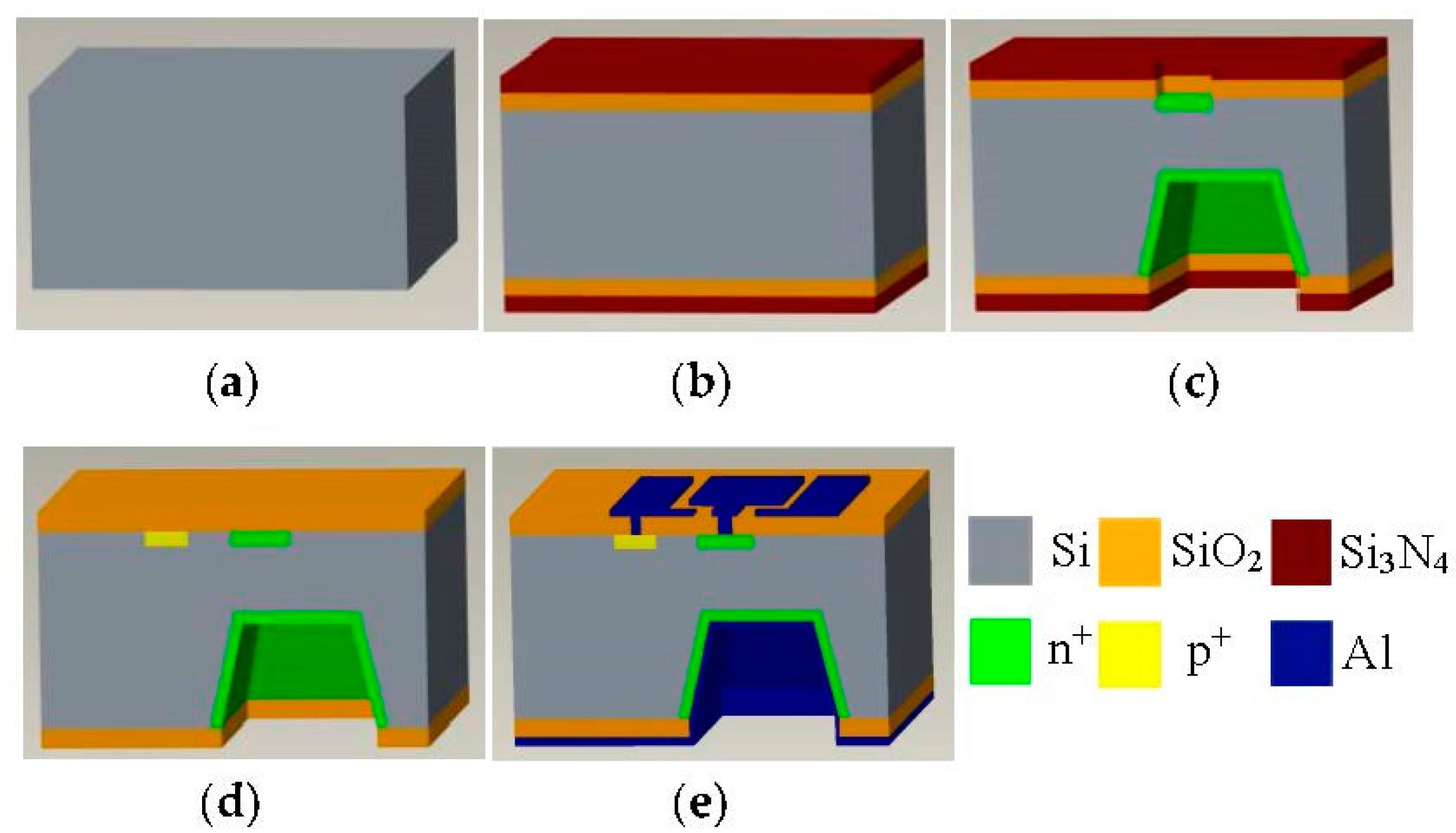
The main fabrication process of the SMSTs is shown in Figure 5, and the processing steps are as follows: (a) cleaning the p-type silicon wafer with a <100> orientation and high resistivity (ρ = 1000 Ω·cm); (b) growing the SiO2 layer (450 nm) by using a thermal oxide method and depositing the Si3N4 layer (200 nm) by low-pressure chemical vapor deposition (LPCVD) on the double-side of the silicon wafer; (c) etching Si3N4 and SiO2 to form a window of the emitter region by first photolithography, then etching a C-type silicon cup with the silicon diaphragm thickness of 30 μm (emitter regions) by the KOH anisotropic etching technique, fabricating the collector region by second photolithography and forming the collector and the emitter regions by diffusing dense phosphorus; (d) photo-etching the base region and etching the double-sided Si3N4 layers and the upper-sided SiO2 layer after diffusing dense boron, and then depositing the single-side of the SiO2 layer; (e) etching contacts of the collector and the base, and depositing an aluminum film on the upper surface by vacuum coating; after that, fabricating the aluminum electrodes of the collector and the base by photography, and then depositing an aluminum film on the bottom to form the aluminum electrode of the emitter and metallizing at 420 °C for a half-hour to form better Ohmic contacts with the base, collector, and emitter. Then, the four chips which have similar characteristics and opposite magnetic sensitive directions are packaged. Figure 6 shows the packaging photograph of the 2D magnetic field sensor based on the SMSTs.
4. Results and Discussion
4.1. Magnetic Sensitive Characteristics of SMSTs
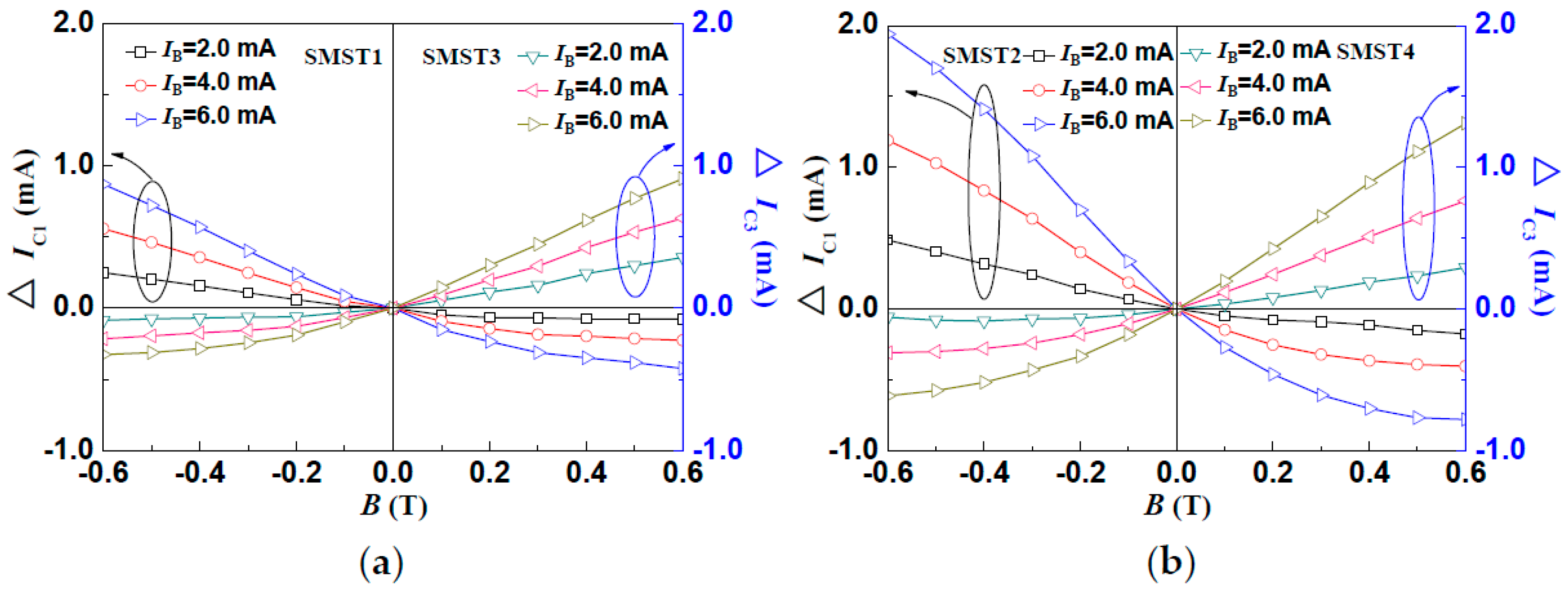
The magnetic sensitive characteristics of the SMSTs were studied by a semiconductor characterization system (4200, KEITHLEY, Cleveland, OH, USA) and a magnetic field generator (CH-100, Cuihaijiacheng Magnetic Technology, Beijing, China) at room temperature. The magnetic sensitive characteristics of the SMST1 and SMST3 were measured under a magnetic field along the x-axis direction, and those of the SMST2 and SMST4 were measured under a magnetic field along the y-axis direction. When the operating current IB = 6.0 mA in a 2D magnetic field range of 0.1 mT–1.2 T, the I–V characteristic curves of the four SMSTs with a resolution of 1 Gs at B = −0.6 T, B = 0 T and B = 0.6 T are shown in Figure 7, respectively.
The experiment results show that, under a constant external supplied voltage, the measured IC1 decreases with the increasing magnetic field, and moves towards the positive direction, while IC3 increases under the same conditions. However, in the subsequent opposite magnetic field direction, the IC1 increases, and the IC3 decreases with the increasing magnetic field. Moreover, under the same conditions, the I–V characteristics of the SMST2 and SMST4 are similar to those of the SMST1 and SMST3, respectively. It indicates that all of the four SMSTs have positive and negative magnetic characteristics. Figure 8a,b shows the relationship curves between the output current (IC1, IC3, IC2, IC4) and B, where the magnetic field ranges from −0.6 T to 0.6 T with a step of 0.1 T. It shows that the measured IC increases not only with a constant operating current but also a constant external magnetic field. When the VCE = 10.0 V and IB = 6.0 mA, the sensitivities of the SMST1, SMST2, SMST3 and SMST4 are 1.08 mA/T, 1.03 mA/T, 1.89 mA/T and 1.92 mA/T, respectively.
4.2. 2D Magnetic Sensitive Characteristics
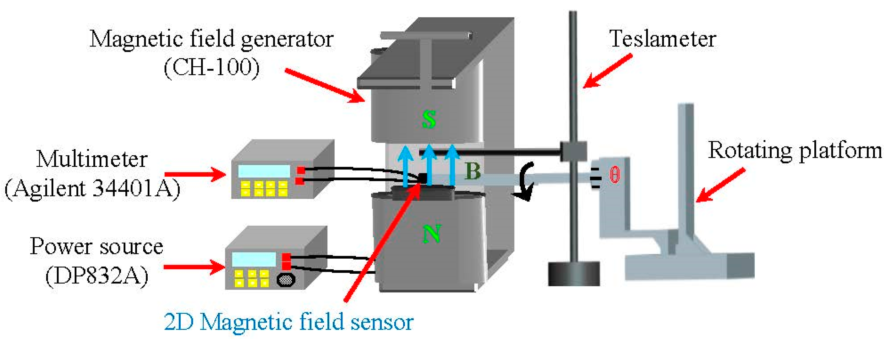
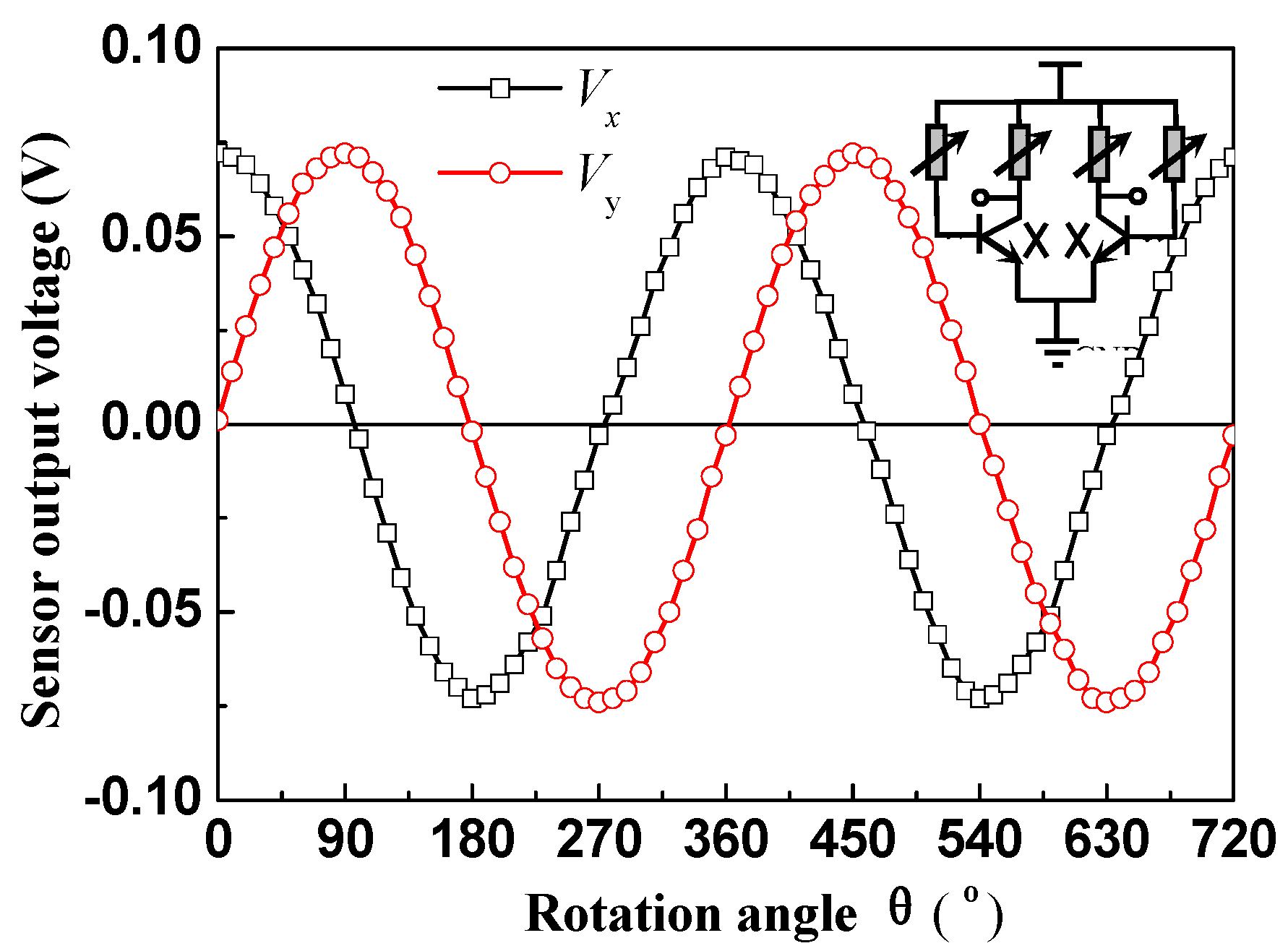
The 2D magnetic sensitive characteristics of the proposed sensor were studied by the rotation platform, magnetic field generator (CH-100), teslameter, multi-meter (Agilent 34401A, Agilent, Santa Clara, CA, USA), and power source (DP832A, RIGOL, Beijng, China), as shown in Figure 9, where the θ is the rotation angle of rotating platform. First, the sensor was fastened on the rotating platform, where the θ is defined as zero when the magnetic induction direction parallel to the sensor surface is along the x axis. At room temperature, the relationship of the sensitivities for the 2D magnetic field sensor at about Vx–θ and Vy–θ was studied by every equivalent circuit respectively, as shown in Figure 4. During the test process, to achieve the same sensitivity of the sensors in the two directions, some external resistors were added between the collector and VDD. When the supply voltage is 10.0 V and the current is 6.0 mA, the characteristic curves of output voltages (Vx and Vy) and θ for the sensor at B = 0.2 T are shown in Figure 10.
The results indicate that under a constant external magnetic field B and operating voltage, θ = 0°, Vx is nearly the maximum and Vy is very small. With an increasing rotation angle θ, Vx is reduced and Vy is increased, gradually. When θ = 90°, Vx is nearly zero and Vy is close to the maximum. When θ = 180°, Vx is nearly the minimum and Vy is nearly zero. When θ = 270°, Vx is nearly zero and Vy is close to the minimum. When θ = 360°, Vx is nearly the maximum and Vy is close to zero. It shows that the output voltages Vx and Vy of the 2D magnetic field sensor regularly follow as the sinusoidal or cosine functions of the rotation angle θ, therefore the direction and the strength of the two-dimensional magnetic field can be measured by the sensor. When θ is a constant, the absolute values of output voltages (Vx and Vy) increase with the B. It indicates that when VDD = 10.0 V and IB = 6.0 mA, the magnetic sensitivities of the sensor in the x and y directions are 360.0 mV/T and 365.0 mV/T, respectively. Equation (9) is the average value expression of the output voltage in the whole period.
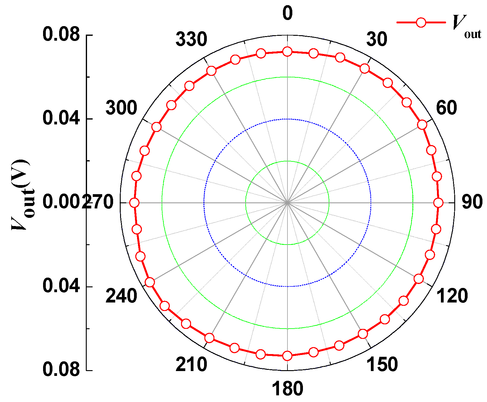
According to Equation (9), under the external magnetic field B, the relationship curves of the output voltage Vout and the rotation angle θ are shown in Figure 11. In the ideal situation, Vout is a constant and the curve is a circle with a radius of 73 mV. The experiment results show that the output voltage Vout changes with the rotation angle θ, attributable to the different characteristics of the four SMSTs in the x and y directions.
In terms of a synthetic analysis of journal articles and experimental results, some designs of 2D magnetic field sensors based on diodes, transistors, and Hall elements are summarized in Table 1. From Table 1, the study of the 2D magnetic field sensor includes Hall components, magnetic diodes and magnetic sensitive transistors, and so on. In this work, a novel 2D magnetic field sensor based on a magnetic sensitive transistor by MEMS technology is designed and fabricated; the magnetic sensitivities in the x and y directions could approach 366.0 mV/T and 365.0 mV/T, respectively. In particular, a referable uniform sensitivity can be measured along the x-axis and y-axis. The study on the novel 2D magnetic field sensor helps to provide a new guide for development in the monolithic integrated magnetic field sensor field.
5. Conclusions
A new type of 2D magnetic field sensor based on the operating principle and characteristics of the silicon magnetic sensitive transistor (SMST) is proposed in this paper. The sensor was composed of two differential structures with four SMSTs. The experiment results show that when the VCE = 10.0 V and IB = 6.0 mA, the magnetic sensitivities of the sensor in the x and y directions reach 366.0 mV/T and 365.0 mV/T, respectively. Based on the differential structure of SMSTs, the 2D magnetic field sensor with a resolution of 1 Gs can measure a 2D magnetic field from 0.1 mT to 1.2 T, not only significantly improving the magnetic sensitivity but also exhibiting a referable uniformity along the x-axis and y-axis.
Acknowledgments
This work is supported by the National Natural Science Foundation of China (61471159), the Natural Science Foundation of Heilongjiang Province (F201433), the University Nursing Program for Young Scholars with Creative Talents in Heilongjiang Province (2015018), and the Postgraduate Innovation Project of Heilongjiang University in China (YJSCX2016-020HLJU).
Author Contributions
Xianghong Yang, Yunjia Bai and Meiwei Lv coordinated the study; Xiaofeng Zhao and Dianzhong Wen designed the sensor device; Xianghong Yang, Yunjia Bai and Meiwei Lv performed the experiments; Xiaofeng Zhao and Xianghong Yang plotted and performed the initial analysis of the data; Xiaofeng Zhao and Xianghong Yang wrote the paper.
Conflicts of Interest
The authors declare no conflict of interest.
References
- Almeida, M.J.; Götze, T.; Ueberschär, O.; Matthes, P.; Müller, M.; Ecke, R.; Exner, H.; Schulz, S.E. Monolithic integration of 2D spin valve magnetic field sensors for angular sensing. Mater. Today Proc. 2015, 2, 4206–4211. [Google Scholar] [CrossRef]
- Roumenin, C.S. 2D magnetodiode sensors based on SOS technology. Sens. Actuators A 1996, 54, 584–588. [Google Scholar] [CrossRef]
- Shapovalov, G.; Chektybayev, B.; Sadykov, A.; Skakov, M.; Kupishev, E. Experimental measurement of magnetic field null in the vacuum chamber of KTM tokamak based on matrix of 2D Hall sensors. Fusion Eng. Des. 2016, 112, 432–439. [Google Scholar] [CrossRef]
- Zhao, X.F.; Li, B.Z.; Wen, D.Z. Fabrication technology and characteristics of a magnetic sensitive transistor with nc-Si:H/c-Si heterojunction. Sensors 2017, 17, 212. [Google Scholar] [CrossRef] [PubMed]
- Roumenin, C.S.; Nikolov, D.; Ivanov, A. A novel parallel-field Hall sensor with low offset and temperature drift 2D integrated magnetometer. Sens. Actuators A 2004, 115, 303–307. [Google Scholar] [CrossRef]
- Lozanova, S.A.; Roumenin, C.S. A novel magnetometer based on a parallel-field silicon Hall sensor. Procedia Chem. 2009, 1, 847–850. [Google Scholar] [CrossRef]
- Zhao, X.F.; Wen, D.Z. Negative-resistance oscillations characteristics of a new type silicon magnetic sensitive transistor on MEMS. J. Semicond. 2005, 6, 1214–1217. [Google Scholar]
- Zhao, X.F.; Wen, D.Z. Fabrication–technology research of new type silicon magnetic-sensitive transistor. Rare Met. Mater. Eng. 2006, 12, 492–494. [Google Scholar]
- Zhao, X.F.; Wen, D.Z.; Pan, D.Y.; Guan, H.Y.; Lv, M.W.; Li, L. Differential structure and characteristics of new type silicon magnetic sensitivity transistor. Chin. Phys. Lett. 2013, 30, 088501. [Google Scholar] [CrossRef]
- Zhao, X.F.; Yang, X.H.; Yu, Y.; Wu, T.; Wen, D. Characteristics of 2D magnetic field sensor based on magnetic sensitivity diodes. Am. Inst. Phys. Adv. 2015, 5, 041321. [Google Scholar] [CrossRef]
- Lozanova, S.; Roumenin, C. Angular position device with 2D low-noise Hall microsensor. Sens. Actuators A 2010, 162, 167–171. [Google Scholar] [CrossRef]
- Yu, C.P.; Sung, G.M. Two-dimensional folded CMOS Hall device with interacting lateral magnetotransistor and magnetoresistor. Sens. Actuators A 2012, 182, 6–15. [Google Scholar] [CrossRef]
- Janković, N.; Pantić, D.; Batcup, S.; Igic, P. A lateral double-diffused magnetic sensitive metal-oxide-semiconductor field-effect transistor with integrated n-type Hall plate. Appl. Phys. Lett. 2012, 100, 263507. [Google Scholar] [CrossRef]
- Lozanova, S.V.; Noykov, S.A.; Ivanov, A.J.; Roumenin, C.S. 2D in-plane Hall sensing based on a new microdevice couple concept. Procedia Eng. 2015, 120, 820–923. [Google Scholar] [CrossRef]
Figure 1.
The cubic structure of the silicon magnetic sensitive transistor. E: emitter; B: base; and C: collector.
Figure 1.
The cubic structure of the silicon magnetic sensitive transistor. E: emitter; B: base; and C: collector.
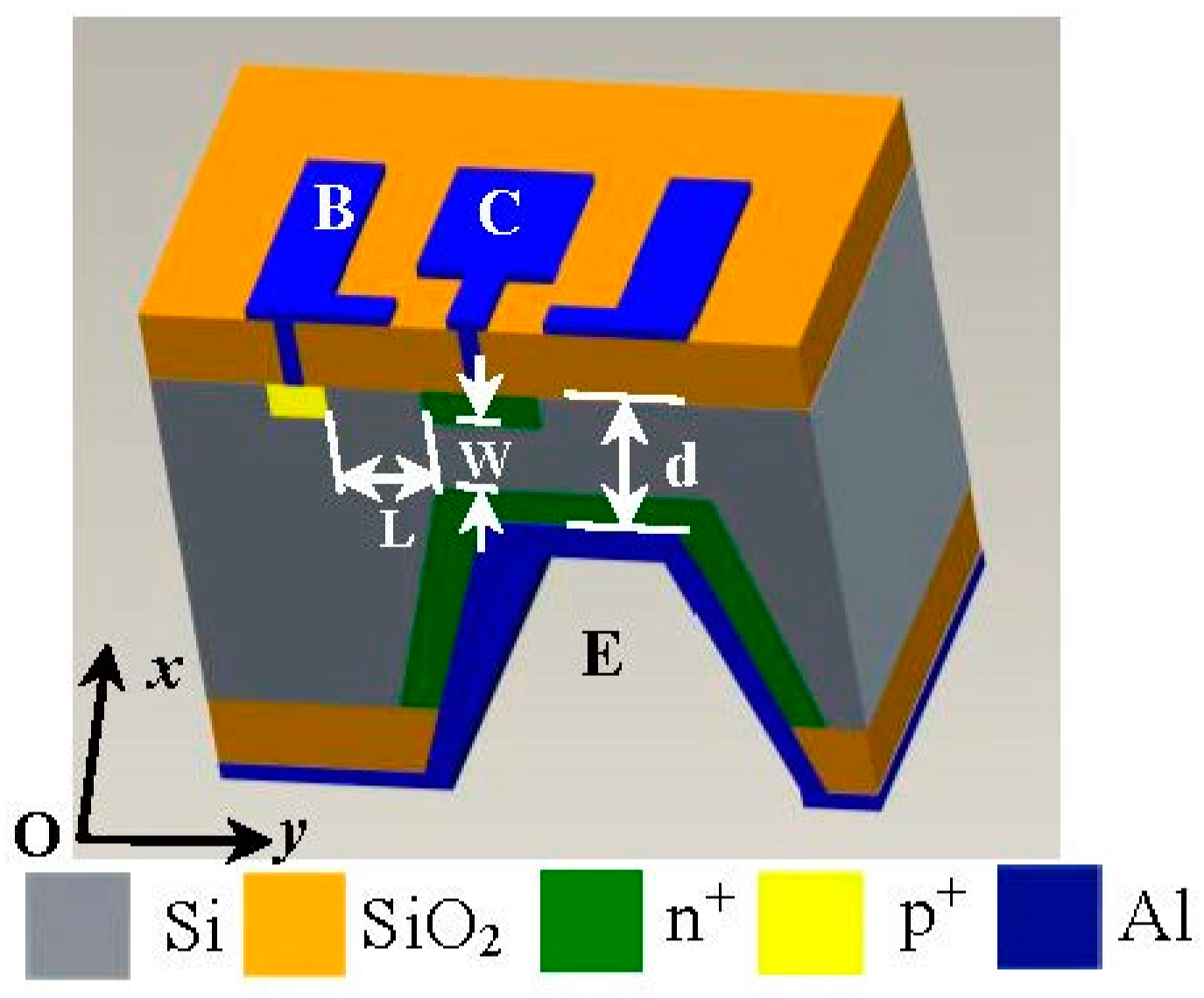
Figure 2.
The basic structure of the two-dimensional (2D) magnetic field sensor: (a) top view; (b) bottom view.
Figure 2.
The basic structure of the two-dimensional (2D) magnetic field sensor: (a) top view; (b) bottom view.

Figure 3.
The operation principle of the silicon magnetic sensitive transistor (SMST) differential structure: (a) B = 0 T; (b) B > 0 T; (c) B < 0 T.
Figure 3.
The operation principle of the silicon magnetic sensitive transistor (SMST) differential structure: (a) B = 0 T; (b) B > 0 T; (c) B < 0 T.

Figure 4.
The equivalent circuit of the 2D magnetic field sensor.

Figure 5.
The fabrication technology of the silicon magnetic sensitive transistor. (a) Cleaning wafer; (b) growing the SiO2 layer and depositing the Si3N4 layer; (c) making the collector and the emitter regions by photolithography; (d) fabricating the base region by photolithography; (e) fabricating the electrodes.

Figure 6.
The packaging photograph of the 2D magnetic field sensor.
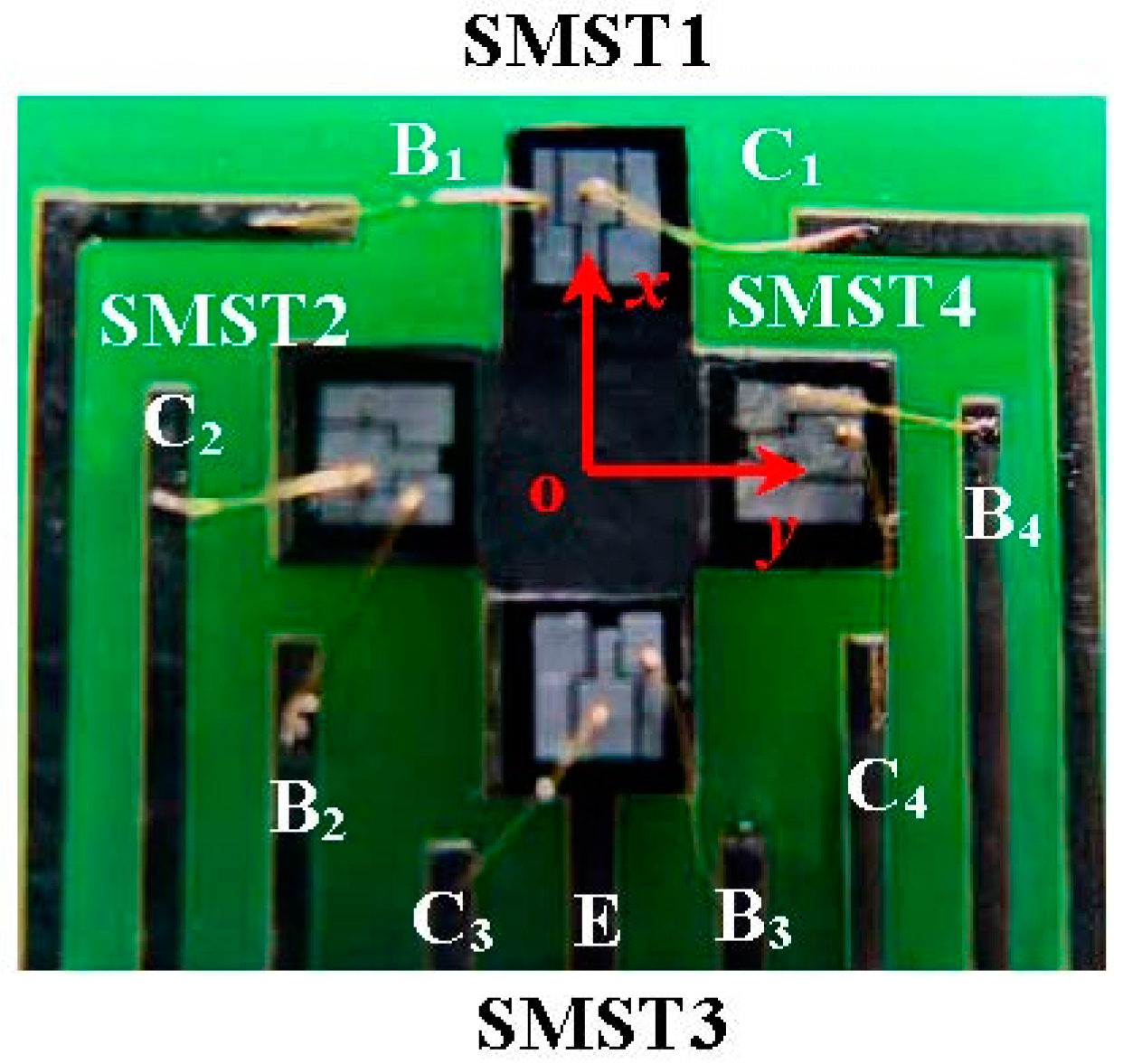
Figure 7.
The I–V characteristic curves of the silicon magnetic sensitive transistor: (a) SMST1; (b) SMST3; (c) SMST2; (d) SMST4.
Figure 7.
The I–V characteristic curves of the silicon magnetic sensitive transistor: (a) SMST1; (b) SMST3; (c) SMST2; (d) SMST4.
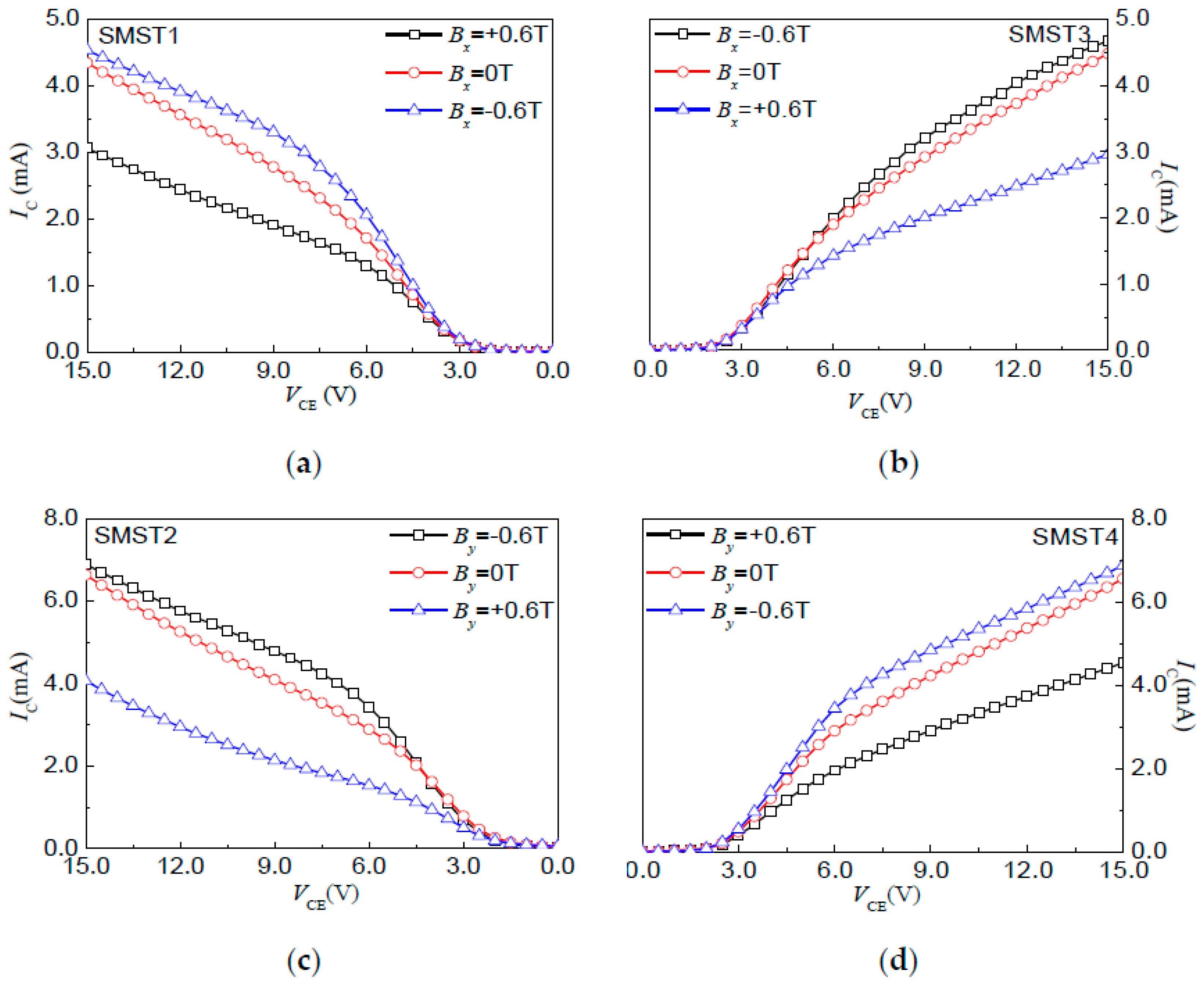
Figure 8.
The ΔIC–B characteristics of the silicon magnetic sensitive transistor: (a) SMST1 and SMST3; (b) SMST2 and SMST4.
Figure 8.
The ΔIC–B characteristics of the silicon magnetic sensitive transistor: (a) SMST1 and SMST3; (b) SMST2 and SMST4.

Figure 9.
Testing system of the 2D magnetic field sensor.

Figure 10.
Characteristic curves of the 2D magnetic field sensor at B = 0.2 T.

Figure 11.
Relationship curves for the output voltage Vout and θ.


Table 1.
Two-dimensional (2D) magnetic field sensors based on magnetic diodes, transistors and Hall elements. SOS: silicon-on-sapphire; CMOS: complementary metal-oxide-semiconductor; IC: integrated circuit; MEMS: micro-electromechanical systems.
Table 1.
Two-dimensional (2D) magnetic field sensors based on magnetic diodes, transistors and Hall elements. SOS: silicon-on-sapphire; CMOS: complementary metal-oxide-semiconductor; IC: integrated circuit; MEMS: micro-electromechanical systems.
| Structure | Technology | Sensitivity | Reference |
|---|---|---|---|
| Magneto-diode | SOS | 0.46 μA/mT | [2] |
| Hall sensor | Simple planar | 41 V/AT, 30 V/AT | [5] |
| Hall sensor | CMOS | 19 V/AT, 19 V/AT | [6] |
| Diode | Bipolar | 544 mV/T, 498 mV/T | [10] |
| Hall device | CMOS | 9.564 mV/T | [12] |
| Transistor a Hall plate | CMOS | 30%/T | [13] |
| Hall element | Bipolar IC | 39 V/AT | [14] |
| Transistor | MEMS | 366 mV/T, 365 mV/T | In this work |
© 2017 by the authors. Licensee MDPI, Basel, Switzerland. This article is an open access article distributed under the terms and conditions of the Creative Commons Attribution (CC BY) license (http://creativecommons.org/licenses/by/4.0/).
Share and Cite
MDPI and ACS Style
Yang, X.; Zhao, X.; Bai, Y.; Lv, M.; Wen, D. Two-Dimensional Magnetic Field Sensor Based on Silicon Magnetic Sensitive Transistors with Differential Structure. Micromachines 2017, 8, 95. https://doi.org/10.3390/mi8040095
AMA Style
Yang X, Zhao X, Bai Y, Lv M, Wen D. Two-Dimensional Magnetic Field Sensor Based on Silicon Magnetic Sensitive Transistors with Differential Structure. Micromachines. 2017; 8(4):95. https://doi.org/10.3390/mi8040095
Chicago/Turabian StyleYang, Xianghong, Xiaofeng Zhao, Yunjia Bai, Meiwei Lv, and Dianzhong Wen. 2017. "Two-Dimensional Magnetic Field Sensor Based on Silicon Magnetic Sensitive Transistors with Differential Structure" Micromachines 8, no. 4: 95. https://doi.org/10.3390/mi8040095
Note that from the first issue of 2016, this journal uses article numbers instead of page numbers. See further details here.