Review

Scanning Micromirror Platform Based on MEMS Technology for Medical Application

by
Eakkachai Pengwang
1,2,*,
Kanty Rabenorosoa
1,
Micky Rakotondrabe
1 and
Nicolas Andreff
1
1
Automatic Control and Micro-Mechatronic Systems Department (AS2M), FEMTO-ST Institute, UMR CNRS 6174-UFC/ENSMM/UTBM, Besancon 25000, France
2
Institute of Field Robotics, King Mongkut’s University of Technology Thonburi, 126 Pracha Uthit Road, Bang Mod, Thung Khru, Bangkok 10140, Thailand
*
Author to whom correspondence should be addressed.
Micromachines 2016, 7(2), 24; https://doi.org/10.3390/mi7020024
Submission received: 1 November 2015 / Accepted: 15 January 2016 / Published: 6 February 2016
(This article belongs to the Special Issue Micro/Nano Robotics)

Abstract

:
This topical review discusses recent development and trends on scanning micromirrors for biomedical applications. This also includes a biomedical micro robot for precise manipulations in a limited volume. The characteristics of medical scanning micromirror are explained in general with the fundamental of microelectromechanical systems (MEMS) for fabrication processes. Along with the explanations of mechanism and design, the principle of actuation are provided for general readers. In this review, several testing methodology and examples are described based on many types of actuators, such as, electrothermal actuators, electrostatic actuators, electromagnetic actuators, pneumatic actuators, and shape memory alloy. Moreover, this review provides description of the key fabrication processes and common materials in order to be a basic guideline for selecting micro-actuators. With recent developments on scanning micromirrors, performances of biomedical application are enhanced for higher resolution, high accuracy, and high dexterity. With further developments on integrations and control schemes, MEMS-based scanning micromirrors would be able to achieve a better performance for medical applications due to small size, ease in microfabrication, mass production, high scanning speed, low power consumption, mechanical stable, and integration compatibility.

1. Introduction

Scanning micromirrors play an important role in modern technology. It involves several principles on many related fields of research, such as micropositioning, micromachining, microscopy, precision measurements, and imprint lithography. Commercial and industrial uses of micromirrors can be found in optical devices, tunable lasers [1], televisions, hard disk storage, projectors, and imaging technologies [2]. The history of scanning micromirrors or digital micromirror device (DMD) began in the year of AD 1987 for an application of digital light projectors (DLP), digital cinema, home entertainment sets, and optomechanical components. The concepts of digital micromirrors are the device that can create images by altering different light sources. The mechanical design of this micromirrors is a silicon micromirrors with a pair of torsion hinges. The capabilities of optical scanning angle of this type are within a range of ±10°. Although the market values of this digital light processing micromirrors are growing for a few decades, the development of micromirrors with advanced techniques is still in progress for higher ranges of motion, faster speed, multi-directions, and broader their applications.
For medical applications, scanning micromirrors have been developed for a submicron biomedical system, such as, optical scanning, microscopy, confocal microscopy, medical endoscopy, laparoscopy, and optical coherence tomography (OCT) [3]. In general, the principal of scanning micromirrors is still the same with the previous technologies; altering the light sources for surgery, scanning the targeted areas, and collecting the bioimaging from the surgical locations. Therefore, design of scanning micromirrors has to be small in volume, inexpensive, and compatible with fiber optic systems [4]. These characteristics are suitable for collecting OCT images of internal architectural morphology and cellular structures in the tissue. Examples of implemented areas include gastrointestinal tract, esophageal, gastric, colonic mucosa, colonic adenoma, respiratory tracts, and carcinoma. While a conventional processes such as computed tomography (CT), positron emission tomography (PET), ultrasound, and magnetic resonance imaging (MRI), can provide a resolution in a range of 100 μm, the optical coherence tomography with micromirrors is reported for a resolution in a range of 10 μm. Indeed, in vivo endoscopic OCT can provide a high penetration depth and high resolution images [4,5]. By implementing an optical coherence reflectometry for a broadband light source, OCT is reported to be a nondestructive, high resolution, and minimally invasive real time imaging method. The method of scanning for OCT can be either linear or rotational. With a further development of signal analysis and noise reduction, OCT can achieved a high speed scanning and high dynamic range for both two-dimensional (2D) and three-dimensional (3D) imaging. This OCT method can be used for cross-sectional imaging for medical, biopsy, and biophotonic applications. However, main challenge of endoscopic OCT is a reliable and accessible of probing low-coherence radiation to the surface of internal organs. In common, flexible fiber optic bundles have been used for endoscopic OCT to access the surgical areas and delivery a light source for surgery. Therefore, the design of scanning micromirrors, distal end, catheter, and the integration of endoscopic OCT needs be done carefully.
Moreover, the development of these scanning micromirrors will enhance capabilities of medical robots for minimally invasive soft tissue surgery, neurosurgery, ear nose and throat (ENT) surgery, phonosurgery, thoracic surgery, cardiac surgery, respiratory tracts surgery, and urologic surgery [6]. A scanning micromirror also improves the development of laser incision processes and skills of physicians. In general, developments of OCT and minimally invasive surgeries (MIS) systems require scanning micromirrors with high resolution, high accuracy, high dexterity, while the dimensions are limited. In common, MIS will involve with a small incision that are enough for fiber optic, endoscopy, and surgical tools. This surgical processes with small incision will result to a faster recovery of patients, less trauma to the body, less blood loss, reduced length of hospital stay. This technique can be enabled by the development of laser surgery and endoscopic imaging by using a scanning micromirror.
Due to the integration constraints of scanning micromirrors, their design, modeling and fabrication have been investigated for the past decades in order to miniaturize and improve the performances. Many successful medical applications have been reported. Common processes to manufacture scanning micromirrors are microelectromechanical systems (MEMS) technology because the processes can create submicron features with high precision, mass productive, and low cost per unit. MEMS-based processes is also suitable for creating biomedical apparatus that require high speed, low power consumption, and high reliability. Several microfabrication techniques are implemented to create scanning micromirrors and their apparatus. Both additive and subtractive processes can be used for the microfabrication of scanning micromirrors. Common substrates can be silicon, glass, thin film of metals, photoresist, and polymer. The most important process is to pattern a substrate by using a photolithography process that is developed previously from semiconductor industries. However, the processes need to be adjusted in order to match the dimensions and requirements for the biomedical applications.
In the literature, there are many research groups that provide solutions for micromirrors with multi-degrees-of-freedom (DOFs). While searching for better solutions, several schematic designs of actuation systems and medical micromirrors are studied for both side-imaging and forward-imaging OCT probes [7]. In general, most of the fabricated devices are based on electrostatic actuators, piezoelectric materials, bimorph materials, and electromagnetic actuators. In order to distinguish among scanning micromirrors and micropositioning devices, several methodologies are recommended. One method to distinguish these devices is by the numbers of allowable motions of the micromirror and types of the motion. Since different applications require different manipulations, this classification can help users to choose a suitable approach. For general microsurgery, a suitable scanning micromirrors should consist of three crucial DOFs; that are two rotational motions around the in-plane axis and one out-of-plane translational motion. Some research groups refer this scanning micromirror type as a tip-tilt-piston mirror. The translation along in-plane motion and the in-plane rotation are not critical since these parameters will not change directions and orientation of laser sources. In order to focus on small micromirrors, this review will focus on scanning micromirrors up to ten millimeters in size in order to emphasize on enabled technology and testing results of scanning micromirrors for biomedical applications.
In this review, classifications of micro-actuators are divided into subgroups with detailed explanations for actuation principles in Section 2. Because each type of biomedical scanning micromirrors has specific microfabrication processes and different mechanism for movement, this section is categorized by the actuation principles with a theoretical explanation and experimental results. This paper also provides recent developments and key fabrication techniques for each type of micro-actuator. For general reader, this review will be a basic guideline on scanning micromirrors and their applications in medical aspects. In Section 3, discussions are given to explain overview of recent technologies, comparisons on performances between each type of micro-actuators, current challenges, and future trends on scanning micromirrors. In Section 4 and Section 5, future work and conclusion are provided for this topical review.

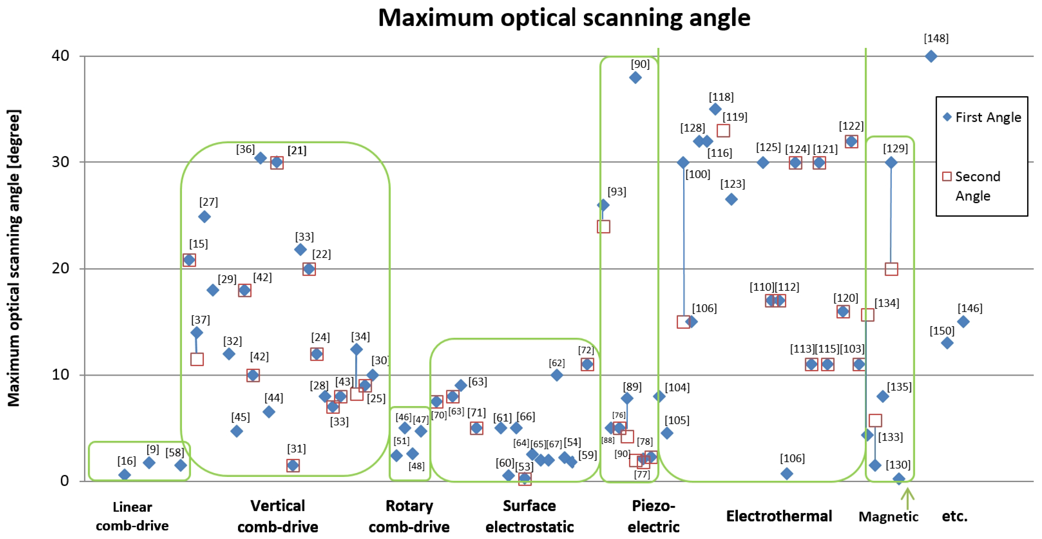
2. Actuation Principles

Many actuators are investigated for scanning micromirrors, for example, electrostatic actuators, piezoelectric actuators, electrothermal actuators, electromagnetic actuators, pneumatic actuators, and shape memory alloy. In this section, reviews of actuation principles are discussed with examples of fabricated devices and relevant work.

2.1. Electrostatic Actuators

Electrostatic actuators are a device that can generate a mechanical motion by a change of stationary electric field in materials. Most of the change in electric charge occurs at the surface of the materials when there is an electrical potential between the two materials. Electrostatic actuators are implemented in many applications such as accelerometers, scanning micromirrors, photonics, televisions, and projectors. For medical application, scanning micromirrors with electrostatic actuators are investigated widely for OCT because they have fast response, large scanning angle, and low power consumption. Microfabrication processes of photolithography, thin film depositions, and high-aspect-ratio etching are usually implemented for electrostatic actuators in micromirror platforms. The common materials include silicon-on-insulator (SOI), monocrystalline silicon, polysilicon, and thin film of metals. These techniques are also implemented with MEMS processes, Multi-User MEMS Processes (MUMPs), and Complementary Metal Oxide Semiconductor (CMOS) developments with process of isotropic, anisotropic, and selective etching. This review summarizes the designs and testing for existing and potential platforms for medical applications. These electrostatic actuators can be classified into four groups; linear comb-drives, vertical comb-drives, rotary comb-drives, and surface electrostatic actuators as shown in Figure 1. Each category has a certain characteristic as explained in the following.
Figure 1. General configurations of electrostatic actuators: (a) linear comb-drives, (b) vertical comb-drives, (c) rotary comb-drives, and (d) parallel-plate actuators. An arrow indicates a motion of electrostatic actuators.
Micromachines 07 00024 g001

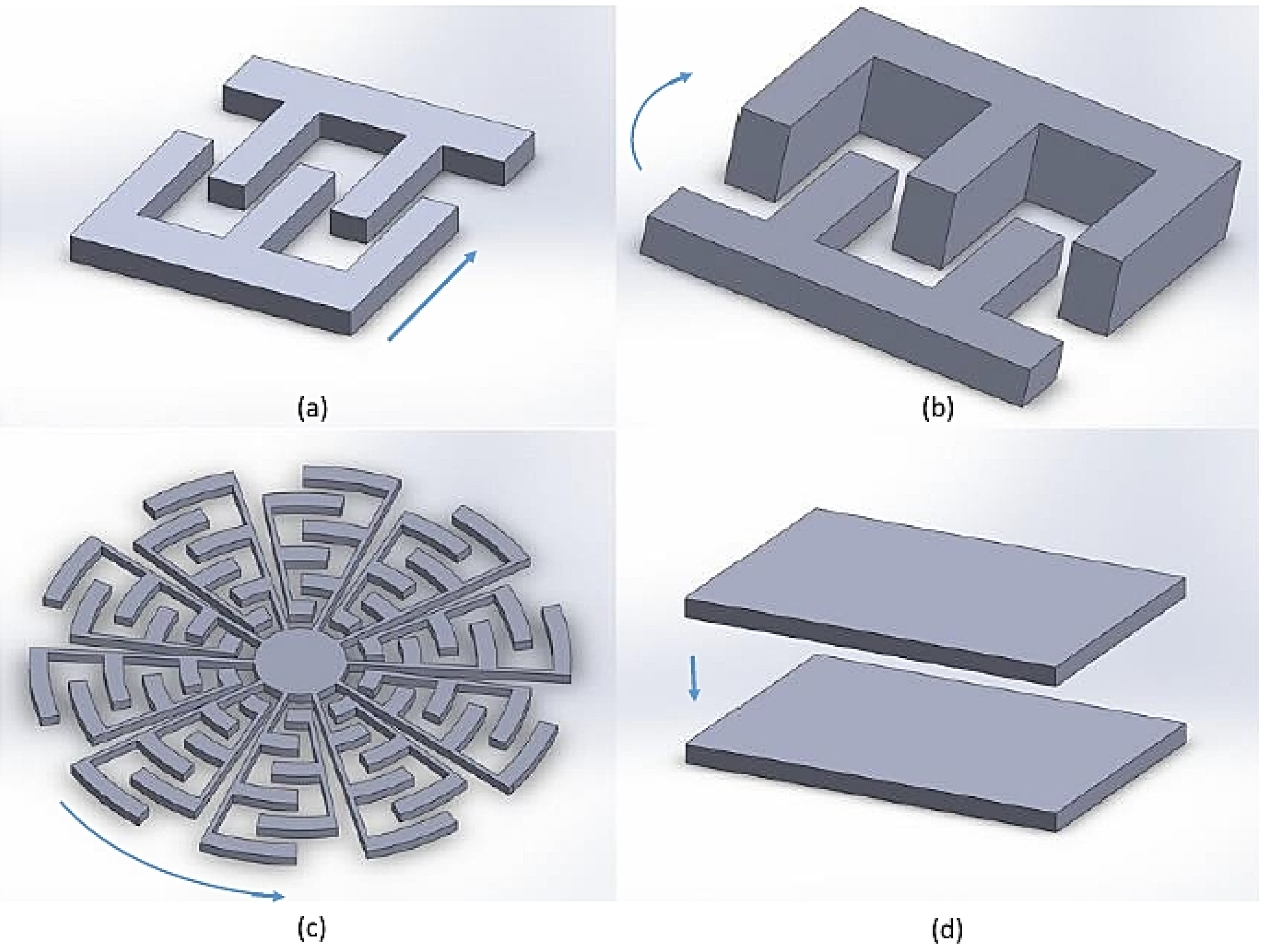
2.1.1. Linear Comb Actuators

Linear comb actuator is a simple electrostatic comb configuration where the actuating direction is the same with the length of comb fingers. The governing equations of motion for general comb-drive actuators involved with parameters on gap between electrodes (d), thickness of comb finger (t), supplied voltage (V), and spring constant for beam suspensions ( k e f f ). The deflection ( δ c o m b ) of comb-drive actuators connected to beam suspensions is depicted with Equation (1).
δ c o m b = F c o m b k e f f = n · ε · t · V 2 d · L 3 4 · E s p r i n g · h · b 3
where F c o m b is the electrostatic force due to comb actuator, n is the number of pairs of comb fingers, ε is permittivity of the media, L is the length of the beam suspension, E is the Young’s modulus of the material, b is the width of the spring, and h is the height of the spring. It is also noted that the height of the device is not influenced on the deflection of linear comb-drives if the thickness of the beam suspension and comb fingers are the same.
Linear electrostatic comb-drives are implemented for several scanning micromirrors with in-plane motions [8,9,10,11,12]. The range of motion is up to 30 μm for two-axis stages. In general, high-aspect-ratio etching such as deep-reactive-ion-etching (DRIE) methods on SOI wafers, is a key for fabrication for these electrostatic actuators. These methods can be used for both creating the structures of linear comb-drives and releasing them from the substrates. Another approach is to implement a compliant actuation with high suspension stiffness for six-DOFs precision manipulator [13]. This device is designed with the micro-assembly of electrostatic actuators with submicron platform. However, the maximum strokes of these actuators are only 20 μm displacement that results to ±10 μm displacement at the end-effector. Another method to combine linear electrostatic actuators with parallel-plate actuators for 3-axis nanopositioning MEMS stage was reported by Liu et al. [14]. By using four sets of comb-drive for in-plane motion and parallel-electrodes for out-of-plane motion, the device was reported for a displacement of ±12.5 μm in the X and Y directions at 30 V and ±3.5 μm in the Z direction at 14.8 V. Moreover, the design of linear comb actuator can be implemented for angular motions of scanning micromirrors. Example of rotational stage is with torsional suspensions on two different layers of SOI substrates that can generate the lateral force for a micromirror [15]. The range of optical deflection angle is ±20.8° for one axis rotation stages. Tung et al. also reported a micro scanner with polydimethylsiloxane (PDMS) flexure joints for a motion range of 0.6° and 5 μm piston motion at 40 V by using linear electrostatic comb actuators [16,17]. Because of high resolution measurements and precision of linear electrostatic comb actuators, they are implemented for other sensor applications as well. Examples are a force sensor to characterize fruit fly flight behavior by using a linear electrostatic comb-drives [18] and nano newtons force-controlled manipulation of biological cells using monolithic MEMS microgripper with two-axis force feedback combs [19]. The device was reported for a force resolution of 38.5 nN and 19.9 nN for contact detection and for gripping, respectively. Additionally, Li et al. presented an electrostatic actuator for optical switch with a 40-μm-displacement of the mirror in VOA applications as well [20].

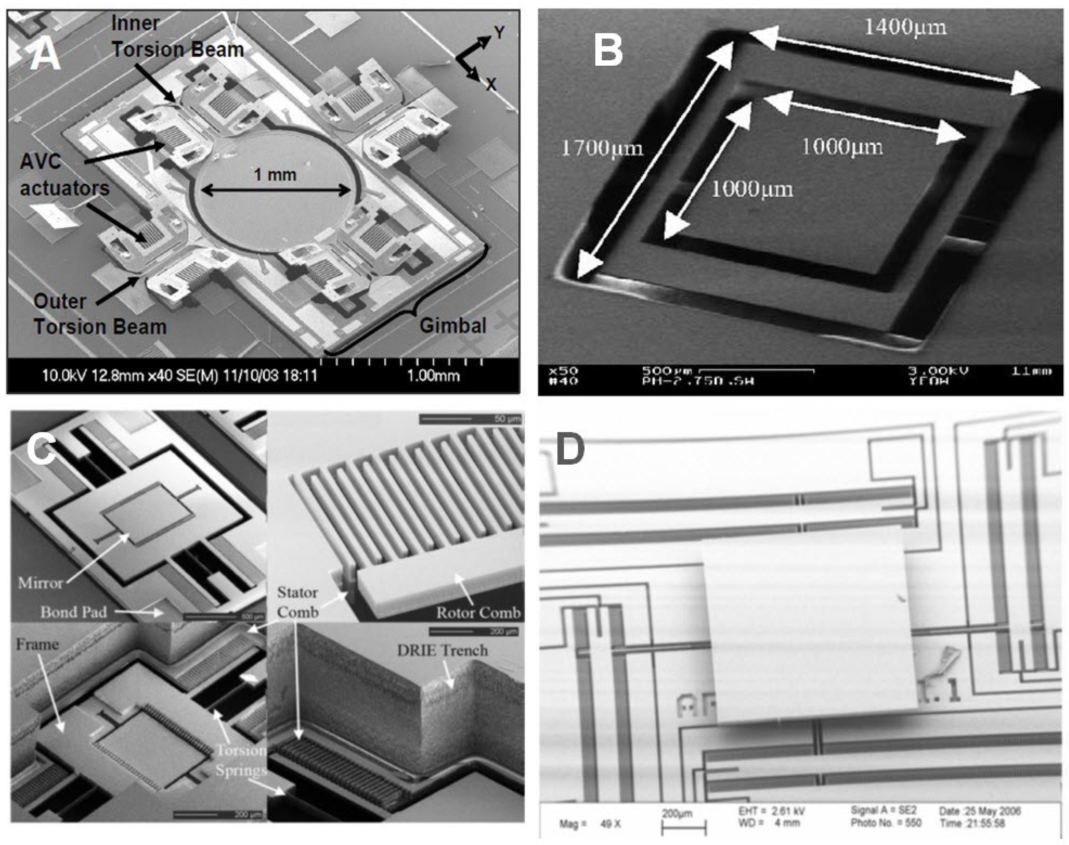
2.1.2. Vertical Comb Actuators

Vertical comb actuators are chosen for both angular stages and transverse-displacement micromirrors. The main characteristic of vertical comb actuator is a direction of the electrostatic force that is perpendicular to the length of comb fingers. This features make it suitable for rotational scanning micromirrors. Many successful devices are demonstrated for vertical electrostatic comb-drives for scanning micromirrors in medical applications. For example, Tien et al. reported an implementation of vertical electrostatic comb-drive for a two-axis MEMS scanning micromirror that can produce up to 30° angles in both axes at frequency greater than 3 kHz [21,22]. With this design, the 3D endoscopic OCT was shown for bioimaging of rabbit trachea, hamster cheek pouch, and cancerous hamster cheek. Further investigations with the same design were also used for in-vivo images of human finger and human vocal cord [23]. With a development of angular vertical comb actuators, group of researchers led by Agguirre et al. demonstrated another design for electrostatic actuators with gimbal structures for 3D in-vivo human skin, lime pulp, and hamster cheek pouch. This device is fabricated using a foundry surface-micromachining, MUMPS, and DRIE processes. With a total dimension of 3 mm × 3 mm, the maximum static mechanical angle is ± 6° in two axes at 160 V. The resonant frequencies of the device are 140 Hz and 463 Hz [24]. Another approach for fabricating vertical comb-drives in scanning micromirrors is to bond a silicon wafer to a SOI wafer [25]. This process was shown by Kumar et al. for a staggered vertical comb-drives for a two-axis scanning micromirror. The device is capable for an optical deflection of ±9° at 110 V with the first resonant frequency of 385 Hz. The validations of this device for OCT imaging were reported for 3D OCT images of human skin and 2D in-vitro biological samples.
There are several potential designs and approaches for a scanning micromirror in medical applications, although they are not tested in clinical trials yet. The simple design is to build vertical electrostatic actuators for angular stages. For one-rotational stages, the maximum angular rotation is 46° with a design of silicon dioxide film, single-crystal silicon, and 1 μm-thick-torsion springs [26]. It is observed that most of the vertical comb-drives were fabricated on SOI wafers with a DRIE processes [27,28,29], and the combined process of DRIE and tetramethylammonium hydroxide (TMAH) [30]. For instance, Hsu et al. reported a flat scanning micromirror fabricated by the combined processes. The devices has a mechanical scan angle of ±10° at 30.8 kHz. Additionally, Molded Surface-micromachining and Bulk Etch Release (MOSBE) process is also investigated for vertical comb-drives with three different heights [31]. This device was reported by Wu et al. for an angular displacement of 1.5° at 35 V. The combined biasing schemes of AC and DC voltages are also crucial for operating vertical comb fingers [32]. Lee et al. demonstrated that vertical comb-drives can achieve an optical deflection angle up to 12° with a combination of 28 V a c and 35 V d c .
For two-rotational micromirrors with vertical comb actuators, Zhou et al. implemented T-shaped torsional beam and off-axis pushing arms with the performances of 15.9° on the inner axis and 13.2° on the outer axis at 71 V [33]. Another two-DOF-rotational micromirror with vertical comb-drives was reported by Piyawattanametha et al. by using MUMPS technology and DRIE processes. The device was demonstrated for bi-directional operations of ±6.2° at 55 V and ±4.1° at 50 V, for the inner and outer gimbals respectively [34,35]. With a fabrication of epitaxial silicon, two-axis MEMS scanning micromirrors can achieve up to ±30.4° dynamic optical scanning angle at 40 V [36]. With V-shaped torsion hinges, the slanted vertical comb-drive can also be developed for the design of two-rotational stages. The device can achieve an optical scanning angles of 11.5° and 14° at 12 V with a resonant frequency of 247 Hz [37].
In addition, vertical comb actuators are used in translational motion for scanning micromirrors. Implementations of micromachined devices with vertical displacement are also used for an gyroscopic applications [38], and capacitive accelerometers [39]. Enabled by SOI MEMS technology, this device can obtain up to 70 μm Z-axis displacement at 1.5 mA. Additionally, Sandner et al. reported a micro scanners with electrostatic comb-drives that can generate up to ±250 μm vertical displacement [40]. This study also investigated two different suspensions of bending springs and pantograph suspension for different performances. Moreover, Wu et al. also reported a 2-DOF optical pick-up head with poly-silicon and silicon nitride (SiN) layers for an upward displacement of 4.6 μm at 30 V and an in-plane displacement of ±16.3 μm at 5 V [41].
For further combinations of rotational and translational stages, various designs are shown in gimbal-less monolithic silicon actuators for tip-tilt-piston. Milavonic et al. demonstrated up to ±30 μ m vertical piston by using three sets of vertical comb-drive actuators. A static optical deflection is 18° at 150 V and a resonant frequency is 4.5 kHz for both axes. Moreover, the device can be manipulated between −10° and 10° optical deflection at 4096 Hz and 1890 Hz for rotation and piston mode [42]. By implementing in-plane actuators, the scanning micromirrors with out-of-plane displacement are investigated for bi-directional tip-tilt-piston mirrors. The design with 3 layers of polysilicon process is used to fabricate a device. The performances were demonstrated for a mechanical tip and tilt angle of ±4° and a piston motion of 5 μm [43]. Another possibility is to integrate bimorph cantilever and vertical comb-drive actuators. Jeong et al. demonstrated this concept for a device with rotational and translational modes. This device can achieve up to 30 μm vertical amplitude at 3.5 kHz and 6.5° on 1 axis-rotation at 830 Hz [44]. Additionally, the 3-DOF stage with a vertical displacement and rotational stage can be up to 62 μm dynamically vertical displacement and ±4.7° angular displacement on both axes with 18 V [45]. This design of micromirror is enable by curled-hinge comb-drives, folded torsional springs, and CMOS structures.

2.1.3. Rotary Comb Actuators

MEMS rotary comb actuator is similar to the linear comb actuator, but the configuration of the comb fingers are located along with the radius of the circular ( r i ) of the device. The mathematical model for rotary comb actuators can be modified as the following equation.
δ c o m b = F c o m b k e f f = ε · t · V 2 · r i / d · k e f f
Examples of rotary comb actuators is demonstrated by Grade et al. for a micromirror on laser-sources tuning devices. This micromirror can scan up to a motion range of 5° [46] by using a two-beam level mechanism with rotary comb-drive actuators. However, this mirror platform is too small for laser spotsize and not suitable for OCT. Zhang et al. reported a rotary comb actuator with one set of comb fingers. With a separation of 2.5 μm between 2-μm-width comb fingers, the device is capable for a rotation angle of 4.7° [47]. It is observed that the flexure hinges are mostly implemented for rotary comb actuators, instead of spring suspension. This design distinguishes rotary comb-drives from other type of electrostatic actuators. Moreover, Yeh et al. reported a full rotary comb actuators based on SOI substrate [48,49]. This full rotary comb actuators can generate a rotational angle of 2.6° at 5 V. For other applications, rotary comb actuators are also investigated for MEMS energy-harvesting device. A rotary comb with 6-mm-diameter, 30 μm thick springs, and 3.6 μm comb gap was designed [50]. In MEMS variable optical attenuator, rotary comb actuators with 2.4-mm-diameter, and 80 μm structural thickness was used [51]. The maximum rotation angle of this device is 2.4°. For the applications of OCT, the rotary comb actuators was proposed by Ayers et al. [52]. This device implements photoresist hinges to assembly a scanning micromirror. However, the validification of this design for OCT are not shown in public yet.

2.1.4. Parallel-Plate Actuators

Parallel-plate electrostatic actuators are alternative for micromirrors in various applications. By using larger surface areas, the designs of scanning micromirror can be developed. Theoretically, electrostatic force of surface electrostatic actuators can be formulated in the following equation.
F s u r f a c e = ε · V 2 · l s u r f · w s u r f / 2 · d 2
where l s u r f and w s u r f are the length and width of surface electrodes. The rests of the parameters are still the same with Equation (1) for linear comb-drives. Example of micromirror with surface electrostatic actuators for 3-D OCT tested in biological samples is demonstrated by Yeow et al. [53]. The device contains a 1.1-μm-thick SiN hinges and surface electrodes. With a platform’s dimension of 1.4 mm × 1.7 mm, the performances of the device are at 0.3° on two axes at 55 V with a resonant frequency of 181 Hz and 45 Hz for outer frame and mirror respectively. Moreover, surface electrostatic actuators can perform up to three DOFs by using a CMOS technique [54]. For a tip-tilt-piston stage, Kao et al. reported an electrostatic phenomenon of parallel plates. This motion can be implemented for micro-manipulation up to 2.1 μm piston stroke and 2.55° tilting angle at 40 V. Example of surface electrostatic actuators for out-of-plane translation are used in many designs [55,56,57,58,59]. For example, micromirrors with surface electrodes can be used to generate up to a 1.2 μm-vertical displacement at 60 V [57]. Pan et al. also reported micromirrors with surface electrostatic actuators with a maximum piston motion of 50 μm at 100 V [55]. Another design by He et al. also demonstrated a repulsive-force for out-of-plane motion with the interdigitated comb configurations [58]. Fabricated by PolyMUMPs technology, this device can achieve a static motion of 86 μm at 200 V and the mechanical rotation range of ±1.5° in two axes.
Surface electrodes are also used for rotational stages for both one DOF and two DOFs. For one-axis micromirrors, the range of motion can be up to 9° for SOI microfabrication [60,61,62,63]. Bulk silicon materials [64,65,66,67] and monocrystalline silicon [68] are also validated for this methodology as well. Examples of one-rotational stages were shown by Hao et al. for a micromirror with a static rotation angle of 3° on both axes at 40 V with the first resonant frequency of 1100 Hz [69]. For two-axis rotation stages, the scanning micromirror can be fabricated on a single-crystalline silicon for an optical scan angle of ±7.5° [70]. Another two-axis mirrors can be fabricated on SOI wafers with a mirror dimension of 750 μm × 800 μm. This device has a mechanically stable operation of ±5° with 60 V [71]. Crystalline silicon with alignment and bonding technique is another technique for a fringe-field tilting mirror with 8° scanning range at 142 V [63]. Additionally, two-axis rotational stage can be implemented with a sidewall electrodes. This fabricated device had a mechanically rotation angle of ±11° in a static mode [72]. Moreover, Zara et al. investigated an integrated force array (IFA) method for OCT scanning in medical applications as well. By using capacitive cells contraction due to electrostatic force, polyimide conductive strips can generate a motion up to 77° and 142° at a resonance of 20.6 Hz and 41.2 Hz and 50° static. The samples of in-vitro porcine colon and eyeball are reported for this device [73,74,75]. Because of the larger area for electrostatic charges, the induced force can be higher. However, the gap distance is also crucial for the design. If the area is larger, the gap distance is always larger and this will reduce the electrostatic force.
To summarize the performances of scanning micromirrors by using electrostatic actuators, Table 1 compares all references from literature reviews based on the subgroup of electrostatic actuators. Moreover, some samples of scanning micromirrors by vertical comb-drives are shown in Figure 2. In addition, Figure 2d shows example of micromirror with surface electrostatic actuators for 3-D OCT tested in biological samples is demonstrated by Yeow et al. [53].
Table 1. Relevant work on micromirrors with electrostatic actuators.
ReferenceYearSize (in mm)CharacteristicsOperating ConditionsNatural Frequency
Linear Comb Actuators
Milanovic et al. [15]20010.7 mirror±20.8° optical (2 axis)90 V2 kHz
Sun et al. [11]20023.2 × 3.04.5 μm, 1.5 μm10 V x , 68 V y -
Li et al. [20]2003-45 μm35 V-
Tung et al. [16]20052.5 × 2.5±0.6°, 5 μm40 V5 kHz
Liu et al. [14]20074 × 412.5, 12.5, 3.5 μm30 V-
Mukhopadhyay et al. [9]2008-1.72°, 18 μm, 18 μm85 V465 Hz
Kim et al. [19]2008-57 μm9 V-
Laszczyk et al. [8]201010 × 1030 μm100 V290 and 550 Hz
Brouwer et al. [13]20104.9 × 5.2 mm20, 20, 20 μm105 V3800 Hz
He et al. [58]20113.2 × 3.2±1.5°, 86 μm200 V1 kHz
Chu et al. [37]20118 × 814°, 11.5°12 V247 Hz
Vertical Comb Actuators
Conant et al. [27]20000.55 dia mirror24.9°250 V34 kHz
Patterson et al. [29]20021 × 1 mirror18°110 V1400 Hz
Xie et al. [38]20020.6 × 0.6270 μm14 V5.08 kHz
Lee et al. [32]20021.5 × 1.2 mirror12°28 V a c , 35 V d c 1353 Hz
Xie et al. [45]20031 × 1 mirror4.7°25 V233 Hz
Milanovic et al. [42]20040.4 × 0.410°, 10°, 30 μm150 V1890 Hz
Lee [36]20041.5 × 1.5±15.2° mech40 V1340 Hz
Jeong et al. [44]20050.3 dia6.5°, 3 μm5.5 V830 Hz
Jung et al. [21]20052.5 × 3 die30° both axis100 V8 kHz
Piyawattanametha et al. [34]2005-12.4° and 8.2°55 V144 Hz
Chong et al. [28]2006-5 V350 Hz
Jung et al. [22]20061.2 mm mirror20° optical100 V2.4 kHz
Wu et al. [31]20060.8 × 0.8 mirror1.5° (2-axis)35 V3.8 kHz
Wu et al. [31]2006-16.3, 16.3, 4.1 μm30 V1900 Hz
Zhou et al. [33]20060.8 × 0.8 mirror21.8° one axis75 V3.6 kHz
Aguirre et al. [24]20073 × 3±6° mech. (2-axis)160 V140 and 463 Hz
Pardo et al. [43]20070.12 × 0.12 mirror8°, 5 μm110 V-
Wu et al. [26]20070.2 × 0.1546°140 V-
Hsu et al. [30]20081 mm dia10° optical100 V30 kHz
Kumar et al. [25]20082 × 2.5 die±9° (2 axis)110 V385 Hz
Sandner et al. [40]20093 dia mirror100 μm44 V500 Hz
1.1 × 1.5250 μm30 V5000 Hz
Rotary Comb Actuators
Ayers et al. [52]2004<1 mm diameter---
Grade et al. [46]20044.3 × 3 chip5°, 300 μm150 V300 Hz
Yeh et al. [48]20063.2 × 4.7 chip2.6°5 V400 Hz
Zhang et al. [47]20071.5 mm long4.7°70 V-
Surface Electrostatic Actuators
Su et al. [70]20010.48 × 0.46 mirror7.5°--
Zara et al. [73,74,75]2002IFA method77° and 142°65 V-
2002(1.5 mirror)50° optical, 146°50 V20.6 Hz
20032 × 2.25 mm---
Niklaus et al. [68]200316 μm × 16 μm0.8 μm gap (one axis)12.5 V-
Greywall et al. [63]2003-142 V-
Greywall et al. [63]2003-210 V-
Dokmeci et al. [71]20040.75 × 0.8 mirror60 V175 Hz
Pan [55]2004-50 μm100 V-
Yeow et al. [53]20051.4 × 1.7-100V45 and 181 Hz
Kudrle et al. [61]200570 × 70 for 1296 mirrors5° mech.160 V78 and 187 Hz
Yan et al. [60]20050.2 × 0.2 mirror0.5°2.7 V50 Hz
Cheng et al. [66]2005-5 μm22.5 V-
Kallweit et al. [64]20060.5 × 0.52.5° (one axis)300 V-
Singh et al. [65]200610 × 1050 V-
Joudrey et al. [67]20068 × 3200 V1000 Hz
Ya’akobovitz et al. [62]20082 × 2 plate10° (one axis)20 V3.8 kHz
Kao et al. [54]200950 μm mirror2.25° both axis40 V59.1 kHz
(Displacement up 2.10 μm)
Hu et al. [57,59]20100.4 × 0.4 mirror1.8°, 1.65 μm100 V2.5 kHz
Zhang et al. [12]2010-30 V-
Bai et al. [72]20101 × 1 mirror11°55 V, 240 V-
Michael et al. [56]20120.2 × 0.8 mirror27 μm17 V-
Figure 2. Several designs of scanning micromirrors with electrostatic actuators: (A) two-axis microelectromechanical systems (MEMS) scanning catheter with vertical comb-drive by Aguirre et al. [24], (B) micromachined 2-D scanner with surface electrostatic actuators by Yeow et al. [53], (C) two-axis MEMS scanning micromirror with staggered vertical comb-drive by Kumar et al. [25], and (D) two-axis MEMS scanning micromirror with vertical comb-drives [23]. Reproduced with permission from [23,24,25,53].
Micromachines 07 00024 g002

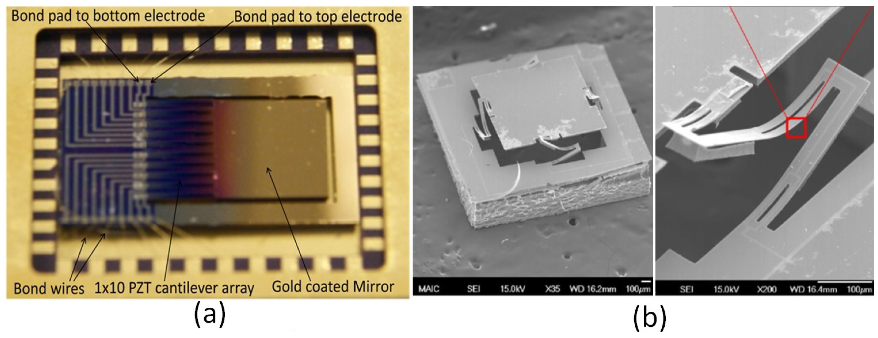
2.2. Piezoelectric Actuators

Piezoelectric actuators are governed by the principle that stress in the material are caused by a change in the electrical field applied to the actuators. Two different material with different piezoelectric properties can be extended or contracted when they are subjected to an electric field. This type of the piezoelectric actuator is known as a bimorph actuator. The other example is when only one material is piezoelectric material, and the other material is not active. This latter type of piezoelectric actuator is also known as a unimorph actuator. Although scanning micromirrors with piezoelectric actuators are not investigated as much as the other types, there are possible solutions for fabricating a scanning micromirror with piezoelectric actuators [76,77]. The advantages of piezoelectric actuators are fast response, low driving voltage, and low power consumption. The common characteristic equation of the piezoelectric actuators are related to the strain mismatch between piezoelectric materials and it can be formulated as shown in Equation (2).
δ p i e z o = C · L 2 t p · ( t p + t x ) · d 31 · V
where δ p i e z o is the deflection of piezoelectric layer, d31 is a piezoelectric charge constant or a polarization generated per unit of mechanical stress applied to a piezoelectric material. C is a constant for each material and V is an applied voltage. L, t p , and t x are length of piezoelectric beam, thickness of piezoelectric layer, and thickness of supporting layer, respectively.
To classify the study on scanning micromirrors with piezoelectric actuators, two groups of researches are distinguished by the processes of formation. One is the scanning micromirrors made from bulk lead zirconate titanate (PZT) material with the final thickness about 20–40 μm. The other is the micromirrors made from thin film PZT with the final thickness in the range of 1–5 μm. Both of them are prepared by different processes in microfabrication techniques and have distinguish characteristics that can be explained in the following.

2.2.1. Bulk Lead Zirconate Titanate (PZT)

The general form of piezoelectric actuator is bulk PZT that can be polished for a thinner component of scanning micromirrors. In general, the thinner PZT can deflect more than the thicker PZT as shown in Equation (2). The typical micromirror platform can be fabricated with this type of piezoelectric materials by the process of chemical or mechanical polishing process. Then, the piezoelectric material can be patterned or etched by combinations of various solutions such as HCl, HNO3, HF, BHF, KOH, NaOH, and NH4Cl. These wet etching processes are fast, easy to implement, and low cost. However, the undercut issues, sidewall profiles, etch rate control, and material selectivity are important challenges for these fabrication processes. Example of a tip-tilt-piston micropositioning stage with the lapping process of bulk PZT substrate was demonstrated by Aktaka et al. [78]. The final thickness of PZT layer is 17 μm and the stage size is 3 mm × 3 mm. The static motion of the device is ±21 μm and ±1.15° under 25 V driving voltage. The first resonant frequency of the device is 0.9 kHz. The maximum power consumption is 450 μW. The design of six-DOF biomedical mirror is also developed of the same design. The device has a maximum static displacement of ±1° for rotation mode, ±7.5 μm for X/Y-displacement mode, and ±22 μm for Z-displacement mode [79]. Moreover, Wilson et al. also reported the mechanical thinning of PZT ceramics with bonding layer of printed circuit board (PCB) adhesive [80]. With the final thickness of 40 μm and 4 mm long, this PZT cantilever can generate ±70 μm displacement. Additionally, Xu et al. described a thinning process for bulk PZT by using wet-etching method in BHF/HCl/NH4Cl solution. In this design, the final thickness of the PZT layer is 40 μm. After the fabrication of the device, arrays of actuators can obtain the maximum deflection of 4.5 μm at 100 V and 21 kHz resonant frequency [81]. With a cantilever of 10 mm-length and 5 μm-thick PZT-Au-Si actuator, the device can deflect up to 200 μm at 100 V and 815 Hz resonant frequency [82]. Even though the thinner thickness of the bulk PZT can be lapped, another crucial issue for bulk PZT fabrication is bonding processes between bulk PZT and base materials. Epoxy materials, such as, solder materials, gold intermediate layer, resin, and benzocyclobutene (BCB) adhesive, and silver paste are developed to glue the base materials to bulk PZT for these processes. Still, the fabrication and integration processes are complicated for scanning micromirrors with higher DOFs.

2.2.2. PZT Thin Film

In order to improve on the performances of the scanning micromirror, PZT thin film are usually implemented using several methods. To deposit PZT thin film, processes in MEMS/CMOS are developed such as arc discharged reactive ion-plating (ADRIP) [83], epitaxial process [84], sol-gel spin-coating [85,86], and sputtering [87]. The thickness of the PZT thin film is generally around 0.4–3 μm. After the deposition, both wet and dry etching processes can be performed to pattern these thin film piezoelectric materials. The wet etching chemicals and processes are similar to those of bulk PZT. In addition, the dry processes can be used for thin film PZT with a combinations of SF6 and CF4 gas with argon gas. These dry process has advantages for low undercut and high resolution, though the selectivity of mask is still challenging for the development of PZT thin film process.
For beam configurations of thin film PZT, sol-gel piezoelectric is common material that are used. Several cantilever designs are implemented for two-dimensional (2D) scanning micromirrors. By using a bending and torsion motion for 3 mm × 3 mm micromirror, Koh et al. reported for sol-gel PZT techniques [88]. The thickness of this PZT beam is 3 μm, and 500 μm in length. Biasing schemes are altered for 10 PZT stripes to generate motion for this design. The first resonant frequency is at 122 Hz and 2.46 kHz for bending and torsional mode. The maximum optical deflection angles are 1.15° and 0.2° for bending and torsional mode at 1.5 V. For a larger micromirror (5 mm × 5 mm), the device can generate higher maximum deflection angles of ±8° at 9 V in bending mode and ±4.6° at 8 V in torsional mode [89]. In addition to a linear cantilever configuration, 2D-scanning micromirrors were investigated with an S-shaped cantilever. With a micromirror size of 1.65 mm × 2 mm, the maximum optical deflection angles at 3 V are ±38.9° and ±2.1° for bending and torsional modes at a resonant frequency of 27 Hz and 70 Hz respectively [90]. A static optical deflection angle of these devices is also reported for 4.6° at 10 V [91]. Moreover, Gilchrist et al. investigated another one rotation micromirror with a combination of thin PZT material, silicon dioxide, and SiN thin film [92]. With a size of 600 μm × 840 μm micromirror, this cantilever had a static angular displacement up to ±7° with a resonant frequencies about 600 Hz.
Moreover, thin film sol-gel piezoelectric actuators were investigated for a 2D micromirror in several configurations. With the PZT thickness of 0.7 μm, the micromirror is connect to with four actuators in the work of Tsaur et al. [93]. The testing results showed a scanning angle range up to 26° with 7.5 V at 3750 Hz. To avoid the deformation of the scanner, two layers of PZT with a thickness of 700 nm can be deposited on both sides of the Pt/Ti layer. Moreover, Smite et al. reported that the design with two actuators can achieve a maximum deflection of 180 μm at 18 V. A static optical angle of this micromirror is up to 40° at 13 V [94]. Additionally, PZT unimorph with a gimbal and flexure hinges are also used for micromirror arrays [95]. This device can move up to ±0.75° at 15 V for X and Y rotation. Further developments by Qui et al. also showed the vertical translational actuators by using thin film PZT as well [96]. By using four of 920 μm × 70 μm beams, this prototype has a performances up to 120 μm static displacement. Nevertheless, PZT material can be implemented in other different ways, for example, H-shaped cavity with three-wafer stack bonding [97], and piezoelectric fiber actuator [98]. Though these methods and technologies are in progress, piezoelectric materials are potential candidates for scanning micromirrors for medical applications with further developments.
Example of a tip-tilt-piston (3-DOFs) micromirror was demonstrated by Zhu et al. for a micromirror based on sol-gel PZT with a thickness of 0.6 μm and silicon dioxide with a thickness of 1 μm [76]. The device is with four piezoelectric unimorph actuators connected to a rectangle micromirror. Each set of lateral shift design consists of three piezoelectric beams made of thin film Pt/Ti/PZT/Pt/Ti/SiO2. The dimension of the scanning micromirror is 1.1 mm × 1.1 mm and a chip footprint is 2 mm × 2 mm. The resonant frequency of the device is at 316 Hz and 582 Hz for the piston and rotation modes. The maximum piston motion at the resonant frequency is about 32 μm and two-dimensional rotating scan ranges are 5° at 2 V. Liu et al. also reported a similar approach with double-S-shaped piezoelectric actuators [77]. The resonant frequency of the rotation modes is at 3.5 kHz. The static motion of the device is 27 μm and ±2° under 5 V driving voltage. The dynamic motion of the device is 109 μm and ±9.65° under 2 V sine wave resonant driving voltage. While the thickness of the piezoelectric is important for the scanning micromirrors, the strength of material and ultimate stress need to be considered for the design as well.
Recent developments of scanning micromirror with piezoelectric actuators are compared in Table 2. Moreover, some examples of scanning micromirrors with piezoelectric actuators are shown in Figure 3.
Figure 3. Several designs of scanning micromirrors with piezoelectric actuators: (a) a piezoelectric actuator in cantilever configuration by Koh et al. [89], and (b) a piezoelectric actuator in parallel kinematics [76]. Reproduced with permission from [76,89].
Micromachines 07 00024 g003
Table 2. Relevant work on micromirrors with piezoelectric actuators.
ReferenceYearSize (in mm)CharacteristicsOperating ConditionsNatural Frequency
Yee et al. [95]20012 × 2±0.75° (2D)±15V-
Tsaur et al. [93]20023 × 326°/24° (2D)15 V3750 Hz
Smits et al. [94]20051.3 × 1.3 mirror40°, 180 μm18 V17.4 kHz
Gao et al. [97]20061 × 1.250.0123 μm7.5 V1.5 kHz
Kim et al. [85]2008-5.5°(X), 4.7°(Y)16 V1.7 kHz
Gilchrist et al. [92]20090.6 × 0.84±7°10 V1–2 kHz
Koh et al. [88]20103 × 3 mirror2° DC/ 5° AC, 35 μm3 V122 Hz
Qiu et al. [96]20101.7 × 1.790 μm20V240 Hz
Zhu et al. [76]20112 × 25° (2D), 32 μm2 V316 Hz
Koh et al. [89]20115 × 5 mirror±8° bending and ±4.6° torsion9 V30 Hz
Koh et al. [90]20114.2 × 5.2±38° bending and ±2° torsion3 V27 Hz
Pan et al. [98]20111 × 1 mirror with fiber17.9°/2.6°400 V6780 Hz
Koh et al. [91]2012-4.6°10 V27 Hz
Liu et al. [77]20132 × 2±2°, 27 μm5 V2.4 kHz
Aktakka et al. [78]20133 × 3 (2.3 mirror)±1.15° (3D), ±21 μm25 V930 Hz

2.3. Electrothermal Actuators

Electrothermal actuator is a micromachined device that can generate a motion by an expansion of materials due to different thermal expansion coefficients of two materials. In general, the change in piezoelectric and thermal property of materials can cause the motion at the same time for bimorph or unimorph material. Theoretically, the deflection of electrothermal cantilevers (ΔL) can be formulated as a function of length of actuators (L), difference on thermal expansion coefficient of two materials (Δα), and temperature difference during operation (ΔT). The equation of motion can be written as shown the following equation.
Δ L = L · Δ α · Δ T
Examples of electrothermal actuators for medical applications include scanning micromirrors, endoscopy, and OCT. The microfabrication processes of electrothermal actuators involves common thin film materials of aluminum, silicon dioxide, polysilicon, and heating metals (such as platinum or tungsten). The classifications of electrothermal actuators can be distinguished into two group by the shapes and its configuration as shown in the following.

2.3.1. Cantilever Micromirror

Various shapes of actuators are investigated for electrothermal actuators. For example, Henneken et al. reported the U- and V-beam thermal actuators [99] with a deflection up to 14 μm. Schweizer et al. demonstrated a two-dimensional micromirror with "L"-shaped cantilever and Physical Vapour Deposition (PVD) hinge [100] for a mechanical scanning range of 15° in two directions. With PVD metal layer, bimorph beam can achieve an out-of-plane motion up to 90° for mechanical scan angles with resonant frequencies between 100 Hz and 600 Hz [101]. Nickel Z-shaped beam was also used for 2-DOF MEMS nanopositioner with eletrothermal actuation [102]. Moreover, Liu et al. reported an electrothermal actuator with a curved concentric connection. The micromirror is connected to four legs of actuators and each leg consists of three sets of bimorph beam. The performances of the device is 11° and 200 μm [103].
Many research groups have also implemented cantilever actuation with several designs and materials. In the early development of bi-axial scanning micromirror, aluminum and silicon dioxide thin film are investigated by Buser et al. The device can provide a deflection angle of 8° at 180 mW with a cantilever structure [104]. In 1995, Buhler demonstrated a bimorph micromirror with aluminum, silicon dioxide, and polysilicon heating. The device is fabricated by ethylenediamine-pyrocatechol (EDP) anisotropic etching. For a size of 40 μm cantilever, the finite element analysis showed a maximum deflection of 14 μm and a rotation angle of 4.6° with 4.6 mW heating power [105]. In 2001, Pan et al. reported array of bimorph of aluminum and silicon dioxide for OCT and two dimensional endoscopy of in vivo porcine bladder through cystectomy [106]. In addition to aluminum and silicon dioxide, SiC cantilever with platinum and NiCr electrodes was reported for electrothermal actuators by Jiang et al. [107]. The resonant frequency of the device is 117 kHz. With a technique of MUMPs process with polysilicon cantilever, buckle-beam structure can obtain a static deflection of 18° at 8 kHz and 160 mW power consumption [108]. Moreover, a semicircular multimorph layer with aluminum-tungsten can be used for electrothermal actuator with low driving voltage at 0.68 V. The allowable scanning angle of the device is 60° at 11 mW power input [109].
Furthermore, a collaborated group of researchers in Singapore investigated a scanning micromirror by implementing electrothermal cantilever combined of silicon, silicon dioxide, and aluminum heater [110]. For a 1.5-μm-thick SOI substrate, a maximum tilting angle is 17° at 1.5 V. The chip size is 1.5 mm × 1.5 mm for a micromirror plate size of 400 μm in diameter. The packaging technique of silicon optical bench (SiOB) was used to assembly this micromirror with a Gradient-index (GRIN) lens for a 4 mm polycarbonate tube [111]. OCT testings of this device can be used to construct 3D images for in vivo and en face diagnostics [112]. Several OCT bioimaging technologies were tested for in-vitro onion [113,114], ex vivo mouse muscle, and mouse skin [115].

2.3.2. Parallel-Connected Micromirror

Another interesting research in electrothermal actuators for endoscopic devices are studied by Professor Huikai Xie. In this design, micromirror cantilevers with aluminum and silicon dioxide mesh were fabricated on a single-crystalline silicon by a DRIE process. The micromirror was reported for 17° at 15 mA. The device has a resonant frequency of 165 Hz with an operating current of 12 mA [116]. In vivo 2D images of porcine bladder [38] and ex-vivo images of rabbit bladder [117] were tested for bioimaging of this device. In 2003, Xie et al. reported an improvement on performances of similar structures with arrays of bimorph actuators for an optical scanning angle of 35°. More images are demonstrated for in vivo diagnosis of rat bladder cancers as well [118]. In similar design, Jain et al. developed a two-axis micromirror with similar structure [119]. The device consists of an orthogonal set of bimorph beam embedded inside the movable frame. The maximum rotation angle of the micromirror and frame is 64° and 33°, respectively. Additionally, miniature endoscopic OCT probe with two axes scanning micromirror can be implemented with three sets of folded bimorph actuators in series [120]. Four sets of these serial bimorph are connected to each sides of a rectangle stage. Bimorph film with Al/SiO2 is used for actuating for a range of ±16° at 3.6 V. The first resonant frequency of the device is 659 Hz. The device has 1.5 mm footprint and 2.6 mm probe diameter. The testings of the device are used for recording images of microspheres in PDMS and rat brain tissue. In 2010, Sun et al. reported further developments of these techniques. The electrothermal actuators consist of 4 legs of rectangle bimorph and 3 arrays for each set [121]. This device has a piston motion of 600 μm at 5.5 V and ±30° motion around both axes for a micromirror of 1 mm × 1 mm. The total footprint of the MEMS micromirror is 2 mm × 2 mm. The device is tested with a Lissajous scan pattern and 3D in vivo images of mouse tongue and ear. Moreover, a piston motion of the micromirror was demonstrated by Izhar et al. by using aluminum, polysilicon electrothermal actuators with embedded heaters, and polysilicon flexural connectors [122]. The device can reach a maximum vertical displacements of 131 μm and rotating angles of 32°. The cut-off frequency of the device is 10.5 Hz with the power consumption of 12 mW.
For scanning micromirrors with translation and rotation, The devices with two sets of bimorph can generate a vertical displacement of 200 μm and a rotation angle of ±15° at 6 V with a size of 0.7 mm × 0.32 mm micromirror [123]. A tip-tilt-piston stage was also demonstrated for a motion of 480 μm in Z-axis and ±30° about X and Y axis for a voltage less than 8 V by using bimorph of aluminum and silicon dioxide (Al/SiO2) and platinum heater [124]. This micromirror has a dimension of 40 μm × 1000 μm × 1000 μm with the first resonant frequencies of 336 Hz. Moreover, a single-crystal silicon micromirror can be used to create sets of bimorph beam to manipulate an inner frame and micromirror. The device with four sets of bimorph were demonstrated with a range of 500 μm piston motion at 15 V and a maximum optical scan angle of 7°. For one degree of rotation, the maximum optical scan angle of the device is 66° at 8.5 V [125]. Wu et al. also demonstrated a tilting angle with three sets of bimorph for a performances of 0.7° tilting angle and 620 μm vertical displacement at 5.3 V [126]. Additionally, Todd et al. reported the use of four inverted-series-connected (ISC) bimorph in rectangle configuration. The device is fabricated by the AMI 1.5 μm CMOS process [127] and the experimental results showed a maximum displacement of 56 μm at temperature of 150°C.
Relevant work on electrothermal actuators for scanning micromirrors are shown in Table 3. Some examples of scanning micromirrors in recent development are shown in Figure 4.
Figure 4. Designs of MEMS scanning micromirror with electrothermal actuators with four sets of actuators: (A) integrated endoscopic probe by Mu et al. [115], (B) by Lzhar et al. [122], (C) by Singh et al. [110], and (D) by Xie et al. [121,124]. Reproduced with permission from [110,115,121,122,124].
Micromachines 07 00024 g004
Table 3. Relevant work on micromirrors with electrothermal actuators.
ReferenceYearSize (in mm)CharacteristicsOperating ConditionsNatural Frequency
Buser et al. [104]1992-180 mW-
Buhler et al. [105]19950.035 × 0.044.5°--
Schweizer et al. [101]1999-90°1 mW330 Hz
Schweizer et al. [100]2000-30°5 mW220 Hz
Pan et al. [106]2001-15°-165 Hz
Xie et al. [38]20021 × 1 mirror32° optical12 mA-
Xie et al. [128]20031 × 1 mirror35° optical7 mA-
Xie et al. [116]20031 × 1 mirror32° optical12 mA165 Hz
Xie et al. [118]20031 × 1 mirror37° optical7 mA-
Jain et al. [119]20041 × 1 mirror64° and 33° (2R)8 mA259 Hz
Jain et al. [123]20050.7 × 0.32 (0.19 mirror)26.5°, ±15, 200 μm6 V1.18 kHz
Todd et al. [127]20060.5 × 0.5 mirror56 μm--
Jiang et al. [107]200650 μm cantilever300 nm0.2 V117 kHz
Henneken et al. [99]20062 mm length13 μm45 V-
Jain et al. [125]20060.5 × 0.5 mirror±30° (2R), 500 μm12 V170 Hz
Singh et al. [110]20081 × 117°, 250 μm2 V-
Xu et al. [112]20082.5 × 2.517° mech.1.5 V46 Hz cut-off
Wu et al. [126]20082.5 × 2.50.7° tilt, 620 μm5.3 V500 Hz
Jia et al. [124]20091 × 1 mirror±30° (2R), 480 μm8 V336 Hz
Premachandran et al. [111]20091.5 × 1.5 chip16°--
Wang et al. [113]20101.5 × 1.511°1.2 V60 Hz
Sun et al. [121]2010-30° (2R), 600 μm5.5 V13 Hz
Mu et al. [115]20111 mm dia. mirror11°1.4 V75 Hz
Pal et al. [109]20111 mm dia. mirror60° (2R)0.6 V104 Hz
Liu et al. [120]20111.5 × 1.5±16° (2 layer flip)3.6 V659 Hz
Izhar et al. [122]20114.5 die 1.332° optical, 131 μm12 mW10.5 Hz cut-off
Liu et al. [103]20122 × 2±11°, 227 μm0.6 V197 Hz

2.4. Magnetic Actuators

A change in electrical field can cause a motion in electromagnetic actuators that can be implemented for medical applications as well. Example of scanning micromirrors with magnetic actuators for OCT is demonstrated by Kim et al. Two-axis magnetically-driven MEMS scanning catheter for endoscopic consists of four folded flexure hinges and a manually-glued neodymium magnet (NdFeB) at the back of the micromachined micromirrors [129]. The device has a range of ±20° in optical scanning angle. The assembled catheter has an outer diameter of 2.8 mm, where contains of coil of American Wire Gauge (AWG) wire for slow and fast coil pairs, GRIN lens, and optical fiber. With this device, in vivo oral cavity tissues and a 3D image of in vivo fingertip were demonstrated. Another example of two-axis micromachined scanners is a nickel-plated magnet on a bulk stainless steel plate in a gimballed cantilever and a gimballed torsional configuration [130]. Enabled by the patterning of stainless steel plate, an electrochemical cell with HCl etching is used to etch the plate and two magnets with a size of 1 mm × 5 mm × 1.5 mm were attached into the frame. The testing results for a gimballed cantilever showed an optical scanning angle of 11.7° and 23.2° in each directional. The device with a gimballed torsional beam can achieve an optical scanning angle of 5.9° and 76° in each directional. Furthermore, electromagnetic MEMS micromirror technology for 3-D optical switching application was demonstrated by Berstein et al. for the mechanical rotation of 8° at 0.75 mA and the first resonant frequency of 96 Hz [131]. Fujita et al. also demonstrated 2-axis MEMS micromirror with SU-8 torsion beam and external samarium–cobalt (SmCo) magnet. The platform has an optical scanning angle up to ±40° for a resonant mode and 5° for a static mode [132]. Ahn et al. also reported a two-DOF stage with current routing by using a single permanent magnet to produce torque from the Lorentz force in the external magnetic field from a single permanent magnet under the micromirror [133]. The device is made of 20-μm-thick chemical mechanical polishing (CMP) silicon, Plasma-Enhanced Chemical Vapor Deposition (PECVD) silicon dioxide, and aluminum thin film. The micromirror dimension is 3.5 mm × 3.5 mm. The device can achieve a maximum angle of rotation of ±1.51° and ±5.71° for micromirror and movable frame with a first resonant frequency of 920 Hz. By electroplating of a copper coil, the optical scanner can be actuated with an external magnetic field as well [134]. The device can achieve ±4.35° for X-axis and ±15.7° for Y-axis at 4.2 V and 1.76 V. Other material, such as, chromium and gold can be patterned for a magnetic coil for micromirror as well. Mitsui et al. reported a device with these multi-layer coil, polyimide insulator, and silicon torsion beams [135]. The device consists of 4 sets and 2 sets of planar coils for Y axis and X-axis on movable plate. The maximum static optical scanning angle of the device is ±8° for a current of ±4.6 mA and ±10.3 mA with the resonant frequency of 106 Hz and 80.5 Hz in X- and Y-axes, respectively.
Although magnetic actuators are used in several medical applications, there are limitations for external magnet and integration processes with magnetic materials. A wide range of research are in progress to investigate the possibilities of creating internal magnet for magnetic actuators. With a microfabrication technique, 10 turns of micro magnetic coil are made of nickel-coated plate and polysilicon torsion bar [136]. The micromirror is attached to the torsion bar and can be manipulated by an out-of-plane excursion and off-chip magnetic field. With a current flow of 500 mA, the device can deflect up to 45° out-of-plane. Several materials are also examined for a magnetic coil used in microfabrication process as well [137]. Jun et al. reported a pattern of copper coil for a high-speed and large-scale electromagnetically actuated resonant MEMS optical scanner [138]. The device has one possible rotation mode with the micromirror area of 6 mm × 4 mm. The maximum optical deflection angle of ±6.8° at 2.95 kHz resonant frequency. Yang et al. demonstrated the copper micromirror that is driven by the eddy-current-induced Lorentz force, whereas the ferromagnetic (electroplated Nickel) micromirror is mainly driven by the magnetostatic force [139]. The optical scanning angle of this device is 20° at an input power of 9 mW and is capable for two-dimensional scanning patterns. Electromagnetic micro-actuator arrays can be made of CoPt planar coil for a thickness of 5–10 μm, however, the maximum deflection is only 1.2 μm [140]. Techniques on micromachined coil are also used in a silicon-lithography-electroforming with a frame of 12 mm × 24 mm and Au electroplating coil [141]. The device has a maximum deflection angle of 9° at 1311 Hz. Moreover, the miniaturization of micro magnetic induction machines is designed for portable application with a micromachined of 1-mm-thick NiFe wafer for a non-laminar stator [142]. A method of pressing between Lithography, Electroplating, and Molding of Polymethylmethacrylate (LIGA PMMA) mold and NdFeB power composite is also alternative for forming a structure [143]. This method can create a permanent magnet with a 5 μm feature size and 200 μm height. Nevertheless, silicon carbide and BCB polymer is also investigated for a rotary micromotor with microball bearing [144].

2.5. Other Actuators

In addition to the described actuators, other types of actuators were discovered for scanning micromirrors as well. Shape memory alloy is one of these alternative micro-actuators for scanning micromirrors [145]. Examples of shape memory alloy for scanning micromirrors were demonstrated by Fu et al. This design of micromirror structure is formed by sputtering TiNi shape memory thin films [146]. With a 3.5-μm-thick-TiNi cantilever on silicon membrane, the micromirror can achieve up to 190 μm vertical displacement at 5 V. With this design, the maximum optical angle is 6°–10°. In addition, Haga et al. reported a miniature pressure sensor for imaging intravascular of human body. In this study, TiNi shape memory alloy (SMA) microcoils were fabricated by photolithography and patterned by etching processes to create an active catheters and guild wires of the device as well [147].
Pneumatic actuators is another choice of micro-actuator for micromirror. Pressure can also manipulate the deformation and displacement of micromirror in several ways. For example, Werber et al. reported a tunable pneumatic micromirror that is embedded on a 50-μm-thick PDMS. The maximum angle of 75° at 65 kPa [148,149]. When combining with thermal actuators, the same group of researchers reported a thermo-pneumatically actuated membrane-based micromirror. The maximum tilting angle of the micromirror is 13° at 30 V (310 °C—temperature). With a formation of seven hexagons of heating locations, the stage can move up to 80 μm for a piston motion [150].
The summary on scanning micromirrors with other type of actuators are shown in Table 4. An example of magnetically-driven scanning micromirrors is shown in Figure 5a. Morevoer, a sample of shap memory alloy is shown in Figure 5b.
Figure 5. Alternative choices for scanning micromirror with (a) magnetic actuators by Kim et al. [129], and (b) shape memory alloy by Fu et al. [146]. Reproduced with permission from [129,146].
Micromachines 07 00024 g005
Table 4. Relevant work on micromirrors with other actuators.
ActuationReferenceYearSize (in mm)CharacteristicsOperating ConditionsNatural Frequency
ElectromagneticCho et al. [134]20020.8 dia. mirror±4.35°, ±15.7°4.2 V/1.7 V-
ElectromagneticAhn et al. [133]20043.5 × 3.5 mirror±1.51°, ±5.71°20 mA920 Hz
ElectromagneticMitsui et al. [135]20067.4 × 9.8±8° static4.6 mA80.5 Hz
ElectromagneticKim et al. [129]20072.4 × 2.9±20° optical3V350 Hz
ElectromagneticGokdel et al. [130]2009-11.7°, 23.2°42 mW350 Hz
PneumaticWerber et al. [148]20062.2 × 2.540°30 kPa-
Thermo-PnWerber et al. [150]20062.2 × 2.513°30 V10 mHz
11 × 1180 μm20 V-
Shape MemoryFu et al. [146]20052.2 × 2.2190 μm (15°)5 V, 30 mA0.1 Hz

3. Discussion

The designs of scanning micromirrors based on MEMS technology are widely investigated for biomedical applications. A suitable design are depended on targeted applications and several parameters, such as size, range of motion, scanning speed, operating voltage, actuator type, and integration processes. These parameters affect the characteristics of MEMS scanning micromirrors in different ways and it can be explained in the following aspects.

3.1. Target Application

With the processes on MEMS/BioMEMS technology, surface micromachining, and selective etching process of substrates, various microscale devices with different mechanisms and designs are fabricated with high precision and high resolution. These processes are attractive for biomedical device because of smaller size, performances, and integration processes. Current research in scanning micromirrors focuses on implementation of micromirrors for endoscopy and OCT. Optical imaging with scanning micromirrors are reported for higher sensitivity, lower light fluence rate, higher speed, and higher resolution. The resolution of OCT is about 2.4 μm and 10 μm for side-imaging and forward-imaging endoscopic OCT. This characteristic is outstanding, compared to conventional methods of imaging such as endoscopic ultrasonography, needle biopsy, electron beam CT, PET, ultrasound, mammography, and MRI. With a development on OCT, medical processes for diagnosis and early detection of diseases can be improve for quality, accessibility, and speed. Examples of bioimaging diagnostics that can be implemented with OCT include gastrointestinal (GI) tract, intravascular system (coronary artery disease), respiratory tract (sleep apnea, laryngeal carcinoma, bronchial inflammation, gynecologic cancers, prostate cancer, and urinary bladder cancer, ovary and uterus tissue, breast cancer and liver biopsies, brain-related disorders (hydrocephalus, cerebral aneurysms) and brain tumors.

3.2. Size

For scanning micromirror, shape and configuration are important parameters that influence performances of endoscopic devices. In general, smaller size will increase the performances of the scanning micromirrors because of smaller weight, less stiffness, and larger natural frequency. Material thickness is also important for the characteristics of scanning micromirrors. Thickness of actuators can affect the performances in two different ways. For electrostatic actuators, thicker comb configurations will increase electrostatic force, but will not affect directly on the deformation of scanning micromirrors because it will cancel to the stiffness of the flexure spring suspension. For other types of micro-actuators, thinner membranes will increase the performances of the scanning micromirror because of the deformation of the actuator can be increased. However, thin membranes and mirrors can be weak for handling and assembling.
The device dimension of scanning micromirrors is a crucial parameter for OCT and biomedical applications. In order to perform minimally invasive endoscopic imaging, scanning micromirror are required to be compact. Typical dimensions of MEMS scanning micromirror ranges from 0.3 μm to 10 mm. However, the overall dimensions that are less than 5 millimeters are preferred for general endoscopic systems. Size of reflected mirror is also important parameter especially for laser surgery. It is also noted that the micromirror dimension should be larger than laser spot size as well.

3.3. Range of Motion

In Figure 6, the average values of micromirror performance for all type of actuators are compared. The performances on maximum optical scanning angle for each type of actuators is shown in Figure 7. Moreover, the values of maximum displacement on piston motion for all type of micromirrors are compared in Figure 8. For the recent development, the average performances of electrostatic actuators are about 12° and 60 μm. Considering each subgroup, the average angular and transverse motion of the vertical comb actuators are higher than that of linear comb-drives, rotary comb-drives, and surface electrostatic. With the average motion of 16° and 80 μm, vertical comb actuators are very attractive for research and development of scanning micromirrors. It is also noted that the rotary comb-drives cannot generate any out-of-plane motion for scanning micromirrors. For linear comb actuators, the maximum range rotation is up to 20° with the translation distance up to 60 μm. The range of natural frequency is between 300–5000 Hz with a maximum operating voltage of 200 V. Among all designs in electrostatic actuators, the maximum value of rotational range is 46° and the maximum piston motion 270 μm that can be achieved by vertical comb-drives. The range of natural frequency for vertical comb actuator is between 150–34,000 Hz with a maximum operating voltage of 250 V. The rotary comb is capable for one rotational movement with the maximum rotation angle of 4.7° at 70 V. Moreover, the parallel-plate actuators can perform up to 5° mechanical angle with a small motion in piston direction. The range of natural frequency for parallel-plate actuators is between 50–59,000 Hz with a maximum operating voltage of 300 V. It is noted that the operating voltage for biomedical devices should not be high. Although some scanning micromirrors are reported for a high performance, they might damage tissues or living cells if the operating voltage is high or the electrical circuit is shorted. The recommended range of voltage for biomedical devices is about 100 V.
For the scanning micromirrors with piezoelectric actuators, the average performances are at 12° and 34 μm for angular motion and out-of-plane motion, respectively. Piezoelectric actuators can perform up to 25° in two axes. The piston motion of piezoelectric actuators can be up to 180 μm with the operating voltage up to 20 V. For the scanning micromirrors with magnetic actuators, the average performances are at 15° and 5 μm for angular motion and out-of-plane motion, respectively.
Figure 6. Comparison on performances for all types of MEMS micro-actuators in scanning micromirrors. The area with sloped-lines represents the averaged value for piston motion. The shaded area represents the average value for rotational angles.
Micromachines 07 00024 g006
Figure 7. Scanning micromirror performances for angular motions. A number in square rectangle is the reference number. The X-axis shows group of actuator types, ranging by year of publications. The Y-axis shows the averages values for the maximum optical scanning angles.
Micromachines 07 00024 g007
Figure 8. Scanning micromirror performances for translational motions. A number in square rectangle is the reference number. The X-axis shows group of actuator types, ranging by year of publications. The Y-axis shows the values for the maximum displacements in piston motion.
Micromachines 07 00024 g008
Among all type of scanning micromirrors, the electrothermal actuators are reported for the best performances in both rotational motions and out-of-plane motion. The average of angular motion are about 27° and 280 μm for piston motion. For electrothermal actuators, the performances of scanning micromirrors can be up to 35° in two axes. The piston motion for electrothermal actuators can be up to 600 μm with the operating voltage up to 50 V. An advantage of electrothermal actuators is initial elevation due to residual stress of material after microfabrication process. Some designs demonstrated an initial elevation of the micromirror platform up to 300 μm. While the searching for better scanning micromirrors, difficulties to fabricate micromirror with multi-DOFs is more than those with a single DOF. It is also observed that for the single-DOF platform, the average of optical scanning angles is larger than the multi-DOF platform.

3.4. Scanning Speed

In Figure 9, the first natural frequency of all micromirrors are plotted. It is observed that the average natural frequency of the electrothermal micromirrors is in the range of 10–1000s Hz, while the average natural frequency of the comb-drives is in the range of 100–10,000s Hz. For piezoelectric actuators, the average natural frequency is in the range of 10–1000s Hz. The response time for dynamic system is about 5 ms for scanning micromirrors implemented in OCT devices.

3.5. Operating Conditions

Operating conditions are also important parameters for testing and implementing the scanning micromirrors. From literature review, several research methodologies and testing devices are used for characterization of MEMS scanning micromirrors. It can be observed that the operating conditions of scanning mirrors can be varied from static responses, dynamic responses, and near-singularity responses. Although all of operating conditions can be controlled with a complex control scheme, the implementations of resonance frequency is more difficult than those of static modes. Due to different behaviors of scanning micromirrors at different frequencies, specific requirements are necessarily considered for implementing micromirrors in biomedical applications.
Figure 9. Scanning micromirror performances based on their first natural frequency. A number in square rectangle is the reference number. The X-axis shows group of actuator types, ranging by year of publications.
Micromachines 07 00024 g009

3.6. Summary

To summarize the advantages and disadvantages for each type of actuators, Table 5 shows the outstanding characteristics of micro-actuators for scanning micromirrors. Challenges for development on electrostatic actuator is pull-in voltage and high driving voltage. Piezoelectric actuators also have issues of charge leakage and hysteresis of materials. For electrothermal and electromagnetic actuators, power consumption is a problem. Moreover, electromagnetic actuators require external magnets that can be large in size and can create electromagnetic interference.
Table 5. Comparisons of micro-actuators for medical scanning mirrors.
Actuation typeAdvantagesDisadvantages
Fast responsePull-in effect
ElectrostaticLow power consumptionHigh driving voltage
Large scan angle
Larger driving forceHigh power consumption
ElectromagneticLower driving voltageExternal magnets
Large scan angleElectromagnetic interference
Fast responsesLarge initial tilting angle
PiezoelectricLarge bandwidthCharge leakage problems
Low power consumptionHysteresis effect
Large scan angleHigh power consumption
ElectrothermalLow driving voltageSlow response
High fill-factor
Because each type of actuators has advantages and disadvantages, the alternative choices for future development are the integrations of various types of actuators. In the literature, several studies focus on combining various types of micro-actuators. Examples of this trend are demonstrated by Zhang et al. for integrated design of thermal actuator with comb-drive electrode for capacitive sensing. This device can achieve an out-of-plane displacement of 24 μm at 17 mW, thermal time constant of 0.24 ms, a mechanical resonant frequency of 16.8 kHz [151]. Moreover, Coa et al. demonstrated an integration of electrothermal and electromagnetic actuator by using a polyMUMPs on SOI wafers [152]. The device is reported for a displacement of 120 μm at 20 Hz.

4. Future Work

Nevertheless, the development of scanning micromirrors for biomedical application is still attractive for engineers and scientists. There are some projects that aim to facilitate the surgery by using scanning micromirrors. Our current project funded by the European Commission’s 7th Framework Program also focuses on cognitive and robotic systems operating in real-world environments. This is an integrative project between several research institutes and clinical laboratories for investigation scanning micromirrors for laser phonomicrosurgery applications. This system consists of a flexible endoscope with an actuated mirror, a stereo-vision and high speed visual servoing, and an augmented reality man-machine interface for assisted teleoperation. (www.microralp.eu) [153,154]. Moreover, there are currently some commercial products of scanning micromirrors that can connect to different applications. This also emphasize the importance of scanning micromirrors for future developments [155,156].

5. Conclusions

Principles of actuation and recent developments that are presented in this paper can assist researchers and scientists for designing. However, the completed system should be evaluated and collaborated with the optics, visions, mechatronics, cognition, and power. With a development of scanning micromirrors for medical applications, capabilities of microsurgery apparatus will be enhanced for better safety, quality of surgical procedures, accessibility of the endoscopic system, dexterity of surgeons, manipulation skills of surgeon as well. According to the types of actuators, scanning micromirrors are studied with electrothermal, electrostatic, piezoelectric, magnetic, shape memory alloy, and pneumatic actuators.
Among the described actuators, electrothermal actuators are widely studied for medical applications. However, the challenges for electrothermal actuators are speed, charge leakage, and hysteresis effect. These issues are investigated and developed by studying of kinematic and control. However, there are still potential actuators that can be used for medical applications, such as electrostatic actuators, and piezoelectric actuators. The combination of more than one type of actuators is also alternative as well.

Acknowledgments

The authors gratefully acknowledge the support by the European Union Seventh Framework Program FP7/2007-2013 - Challenge 2 - Cognitive Systems and Robotics - under grant agreement μRALP - n°288233. Moreover, this work has been supported by the Labex ACTION project (contract “ANR-11-LABX-01-01”), the French Agence Nationale de la Recherche, through the LEMA project (contract “ANR-12-BS03 007 01”), and the French RENATECH network and its FEMTO-ST technological facility.

Author Contributions

Eakkachai Pengwang mainly collected data, analyzed data, and prepared the manuscript. Kanty Rabenorosoa, Micky Rakotondrabe and Nicolas Andreff gave technical support and conceptual advices for this topical review. All authors discussed the results and implications and commented on the manuscript at all stages.

Conflicts of Interest

The authors declare no conflict of interest.

References

  1. Liu, A.Q.; Zhang, X.M. A review of MEMS external-cavity tunable lasers. J. Micromech. Microeng. 2007, 17, R1. [Google Scholar] [CrossRef]
  2. Dudley, D.; Duncan, W.M.; Slaughter, J. Emerging digital micromirror device (DMD) applications. Proc. SPIE 2003, 4985, 14–25. [Google Scholar]
  3. Liu, A.Q.; Zhang, X.M. MEMS-based endoscopic optical coherence tomography. Int. J. Opt. 2011, 2011, 825629. [Google Scholar]
  4. Tearney, G.J.; Brezinski, M.E.; Bouma, B.E.; Boppart, S.A.; Pitris, C.; Southern, J.F.; Fujimoto, J.G. In vivo endoscopic optical biopsy with optical coherence tomography. Science 1997, 276, 2037–2039. [Google Scholar] [CrossRef] [PubMed]
  5. Jackle, S.; Gladkova, N.; Feldchtein, F.; Terentieva, A.; Brand, B.; Gelikonov, G.; Gelikonov, V.; Sergeev, A.; Fritscher-Ravens, A.; Freund, J.; et al. In vivo endoscopic optical coherence tomography of the human gastrointestinal tract-toward optical biopsy. Endoscopy 2000, 32, 743–749. [Google Scholar] [CrossRef] [PubMed]
  6. Dogangil, G.; Davies, B.L.; Y Baena, F.R. A review of medical robotics for minimally invasive soft tissue surgery. J. Eng. Med. 2010, 224, 653–679. [Google Scholar] [CrossRef]
  7. Yaqoob, Z.; Wu, J.; McDowell, E.J.; Heng, X.; Yang, C. Methods and application areas of endoscopic optical coherence tomography. J. Biomed. Opt. 2006, 11, 063001. [Google Scholar] [CrossRef] [PubMed]
  8. Laszczyk, K.; Bargiel, S.; Gorecki, C.; Krezel, J.; Dziuban, P.; Kujawinskab, M.; Callet, D.; Frank, S. A two directional electrostatic comb-drive XY micro-stage for MOEMS applications. Sens. Actuators A Phys. 2010, 163, 255–265. [Google Scholar] [CrossRef]
  9. Mukhopadhyay, D.; Dong, J.; Pengwang, E.; Ferreira, P. A SOI-MEMS-based 3-DOF planar parallel-kinematics nanopositioning stage. Sens. Actuators A Phys. 2008, 147, 340–351. [Google Scholar] [CrossRef]
  10. Sun, Y.; Piyabongkarn, D.; Sezen, A.; Nelson, B.J.; Rajamani, R. A high-aspect-ratio two-axis electrostatic microactuator with extended travel range. Sens. Actuators A Phys. 2002, 102, 49–60. [Google Scholar] [CrossRef]
  11. Sun, Y.; Piyabongkarn, D.; Sezen, A.; Nelson, B.J.; Rajamani, R.; Schoch, R.; Potasek, D.P. A novel dual-axis electrostatic microactuation system for micromanipulation. In Proceedings of 2002 IEEE/RSJ International Conference on Intelligent Robots and Systems, EPFL, Switzerland, 30 September– 4 October 2002; Volume 2, pp. 1796–1801.
  12. Zhang, Q.; Zhang, J.; Yu, M.; Tan, C.W.; Lo, G.Q.; Kwong, D.L. A two-wafer approach for integration of optical MEMS and photonics on silicon substrate. IEEE Photon. Technol. Lett. 2010, 22, 269–271. [Google Scholar] [CrossRef]
  13. Brouwer, D.M.; Jong, B.R.D.; Soemers, H.M.J. Design and modeling of a six DOFs MEMS-based precision manipulator. Precision Eng. 2010, 34, 307–319. [Google Scholar] [CrossRef]
  14. Liu, X.; Kim, K.; Sun, Y. A MEMS stage for 3-axis nanopositioning. J. Micromech. Microeng. 2007, 17, 1796. [Google Scholar] [CrossRef]
  15. Milanovic, V.; Last, M.; Pister, K.S.J. Monolithic silicon micromirrors with large scanning angle. In Proceedings of IEEE/LEOS International Conference on Optical MEMS (Optical MEMS 2001), Okinawa, Japan, 25–28 September 2001.
  16. Tung, Y.C.; Kurabayashi, K. A single-layer PDMS-on-silicon hybrid microactuator with multi-axis out-of-plane motion capabilities-Part I: design and analysis. J. Microelectromech. Syst. 2005, 14, 548–557. [Google Scholar] [CrossRef]
  17. Tung, Y.C.; Kurabayashi, K. A single-layer PDMS-on-silicon hybrid microactuator with multi-axis out-of-plane motion capabilities-part II: fabrication and characterization. J. Microelectromech. Syst. 2005, 14, 558–566. [Google Scholar] [CrossRef]
  18. Sun, Y.; Fry, S.N.; Potasek, D.; Bell, D.J.; Nelson, B.J. Characterizing fruit fly flight behavior using a microforce sensor with a new comb-drive configuration. J. Microelectromech. Syst. 2005, 14, 4–11. [Google Scholar] [CrossRef]
  19. Kim, K.; Liu, X.; Zhang, Y.; Sun, Y. Nanonewton force-controlled manipulation of biological cells using a monolithic MEMS microgripper with two-axis force feedback. J. Micromech. Microeng. 2008, 18, 055013. [Google Scholar] [CrossRef]
  20. Li, J.; Zhang, Q.X.; Liu, A.Q. Advanced fiber optical switches using deep RIE (DRIE) fabrication. Sens. Actuators A Phys. 2003, 102, 286–295. [Google Scholar] [CrossRef]
  21. Jung, W.; Zhang, J.; Wang, L.; Wilder-Smith, P.; Chen, Z.; McCormick, D.T.; Tien, N.C. Three-dimensional optical coherence tomography employing a 2-axis microelectromechanical scanning mirror. IEEE J. Sel. Top. Quant. Electron. 2005, 11, 806–810. [Google Scholar] [CrossRef]
  22. Jung, W.; McCormick, D.T.; Zhang, J.; Wang, L.; Tien, N.C.; Chen, Z. Three-dimensional endoscopic optical coherence tomography by use of a two-axis microelectromechanical scanning mirror. Appl. Phys. Lett. 2006, 88, 163901. [Google Scholar] [CrossRef]
  23. McCormick, D.T.; Jung, W.; Ahn, Y.C.; Chen, Z.; Tien, N.C. A three dimensional real-time MEMS based optical biopsy system for in-vivo clinical imaging. In Proceedings of 2007 International Solid-State Sensors, Actuators and Microsystems Conference (TRANSDUCERS 2007), Lyon, France, 10–14 June 2007; pp. 203–208.
  24. Aguirre, A.D.; Hertz, P.R.; Chen, Y.; Fujimoto, J.G.; Piyawattanametha, W.; Fan, L.; Wu, M.C. Two-axis MEMS scanning catheter for ultrahigh resolution three-dimensional and en face imaging. Opt. Express 2007, 15, 2445–2453. [Google Scholar] [CrossRef] [PubMed]
  25. Kumar, K.; Condit, J.C.; McElroy, A.; Kemp, N.J.; Hoshino, K.; Milner, T.E.; Zhang, X. Fast 3D in vivo swept-source optical coherence tomography using a two-axis MEMS scanning micromirror. J. Opt. A Pure Appl. Opt. 2008, 10, 044013. [Google Scholar] [CrossRef]
  26. Wu, W.G.; Chen, Q.H.; Yan, G.Z.; Yin, D.Q.; Chen, Z.Y.; Hao, Y.L.; Xu, A.S.; Wang, Y.Y. Micro torsion mirror actuated by compound electrostatic driving structure. Sens. Actuators A Phys. 2007, 135, 758–764. [Google Scholar] [CrossRef]
  27. Conant, R.A.; Nee, J.T.; Lau, K.Y.; Muller, R.S. A flat high-frequency scanning micromirror. In Proceedings of 2000 Solid-State Sensor and Actuator Workshop, Hilton Head Island, SC, USA, 2–7 June 2002; pp. 6–9.
  28. Chong, C.; Isamoto, K.; Toshiyoshi, H. Optically modulated MEMS scanning endoscope. IEEE Photon. Technol. Lett. 2006, 18, 133–135. [Google Scholar] [CrossRef]
  29. Patterson, P.R.; Hah, D.; Nguyen, H.; Toshiyoshi, H.; Chao, R.m.; Wu, M.C. A scanning micromirror with angular comb drive actuation. In Proceedings of The 15th IEEE International Conference on Micro Electro Mechanical Systems (MEMS 2002), Las Vegas, NV, USA, 20–24 January 2002; pp. 544–547.
  30. Hsu, S.; Klose, T.; Drabe, C.; Schenk, H. Fabrication and characterization of a dynamically flat high resolution micro-scanner. J. Opt. A Pure Appl. Opt. 2008, 10, 044005. [Google Scholar] [CrossRef]
  31. Wu, M.; Fang, W. A molded surface-micromachining and bulk etching release (MOSBE) fabrication platform on (1 1 1) Si for MOEMS. J. Micromech. Microeng. 2006, 16, 260. [Google Scholar] [CrossRef]
  32. Lee, J.H.; Ko, Y.C.; Jeong, H.M.; Choi, B.S.; Kim, J.M.; Jeon, D.Y. SOI-based fabrication processes of the scanning mirror having vertical comb fingers. Sens. Actuators A Phys. 2002, 102, 11–18. [Google Scholar] [CrossRef]
  33. Zhou, L.; Kahn, J.M.; Pister, K.S.J. Scanning micromirrors fabricated by an SOI/SOI wafer-bonding process. J. Microelectromech. Syst. 2006, 15, 24–32. [Google Scholar] [CrossRef]
  34. Piyawattanametha, W.; Patterson, P.R.; Hah, D.; Toshiyoshi, H.; Wu, M.C. Surface-and bulk-micromachined two-dimensional scanner driven by angular vertical comb actuators. J. Microelectromech. Syst. 2005, 14, 1329–1338. [Google Scholar] [CrossRef]
  35. Ra, H.; Piyawattanametha, W.; Taguchi, Y.; Lee, S.; Mandella, M.J.; Solgaard, O. Two-dimensional MEMS scanner for dual-axes confocal microscopy. J. Microelectromech. Syst. 2007, 16, 969–976. [Google Scholar] [CrossRef]
  36. Lee, C. Design and fabrication of epitaxial silicon micromirror devices. Sens. Actuators A Phys. 2004, 115, 581–590. [Google Scholar] [CrossRef]
  37. Chu, H.M.; Hane, K. Design, fabrication and vacuum operation characteristics of two-dimensional comb-drive micro-scanner. Sens. Actuators A Phys. 2011, 165, 422–430. [Google Scholar] [CrossRef]
  38. Xie, H.; Fedder, G.K. Vertical comb-finger capacitive actuation and sensing for CMOS-MEMS. Sens. Actuators A Phys. 2002, 95, 212–221. [Google Scholar] [CrossRef]
  39. Tsuchiya, T.; Funabashi, H. A z-axis differential capacitive SOI accelerometer with vertical comb electrodes. Sens. Actuators A Phys. 2004, 116, 378–383. [Google Scholar] [CrossRef]
  40. Sandner, T.; Drabe, C.; Schenk, H.; Kenda, A. Large stroke MOEMS actuators for optical path length modulation in miniaturized FTIR spectrometers. Proc. SPIE 2009, 7319, 73190H. [Google Scholar]
  41. Wu, M.; Fang, W. A molded surface-micromachining and bulk etching release (MOSBE) fabrication platform on (1 1 1) Si for MOEMS. J. Micromech. Microeng. 2006, 16, 260. [Google Scholar] [CrossRef]
  42. Milanovic, V.; Matus, G.A.; McCormick, D.T. Gimbal-less monolithic silicon actuators for tip-tilt-piston micromirror applications. IEEE J. Sel. Top. Quant. Electron. 2004, 10, 462–471. [Google Scholar] [CrossRef]
  43. Pardo, F.; Cirelli, R.A.; Ferry, E.J.; Lai, W.Y.C.; Klemens, F.P.; Miner, J.F.; Pai, C.S.; Bower, J.E.; Mansfield, W.M.; Kornblit, A.; et al. Flexible fabrication of large pixel count piston-tip-tilt mirror arrays for fast spatial light modulators. Microelectron. Eng. 2007, 84, 1157–1161. [Google Scholar] [CrossRef]
  44. Jeong, K.H.; Lee, L.P. A novel microfabrication of a self-aligned vertical comb drive on a single SOI wafer for optical MEMS applications. J. Micromech. Microeng. 2005, 15, 277–281. [Google Scholar] [CrossRef]
  45. Xie, H.; Pan, Y.; Fedder, G.K. A CMOS-MEMS mirror with curled-hinge comb drives. J. Microelectromech. Syst. 2003, 12, 450–457. [Google Scholar]
  46. Grade, J.D.; Yasumura, K.Y.; Jerman, H. Advanced, vibration-resistant, comb-drive actuators for use in a tunable laser source. Sens. Actuators A Phys. 2004, 114, 413–422. [Google Scholar] [CrossRef]
  47. Zhang, X.M.; Liu, A.Q.; Tamil, J.; Yu, A.; Cai, H.; Tang, D.Y.; Lu, C. Real pivot mechanism of rotary comb-drive actuators for MEMS continuously tunable lasers. In Proceedings of 2007 International Solid-State Sensors, Actuators and Microsystems Conference (TRANSDUCERS 2007), Lyon, France, 10–14 June 2007; pp. 1437–1440.
  48. Yeh, J.A.; Jiang, S.S.; Lee, C. MOEMS variable optical attenuators using rotary comb drive actuators. IEEE Photon. Technol. Lett. 2006, 18, 1170–1172. [Google Scholar] [CrossRef]
  49. Yeh, J.A.; Chen, C.N.; Lui, Y.S. Large rotation actuated by in-plane rotary comb-drives with serpentine spring suspension. J. Micromech. Microeng. 2005, 15, 201. [Google Scholar] [CrossRef]
  50. Yang, B.; Lee, C.; Kotlanka, R.K.; Xie, J.; Lim, S.P. A MEMS rotary comb mechanism for harvesting the kinetic energy of planar vibrations. J. Micromech. Microeng. 2010, 20, 065017. [Google Scholar] [CrossRef]
  51. Lim, T.S.; Ji, C.H.; Oh, C.H.; Kwon, H.; Yee, Y.; Bu, J.U. Electrostatic MEMS variable optical attenuator with rotating folded micromirror. IEEE J. Sel. Top. Quant. Electron. 2004, 10, 558–562. [Google Scholar] [CrossRef]
  52. Ayers, J.A.; Tang, W.C.; Chen, Z. 360 rotating micro mirror for transmitting and sensing optical coherence tomography signals. In Proceedings of 2004 IEEE Sensors, Vienna, Austria, 24–27 October 2004; pp. 497–500.
  53. Yeow, J.T.W.; Yang, V.X.D.; Chahwan, A.; Gordon, M.L.; Qi, B.; Vitkin, I.A.; Wilson, B.C.; Goldenberg, A.A. Micromachined 2-D scanner for 3-D optical coherence tomography. Sens. Actuators A Phys. 2005, 117, 331–340. [Google Scholar] [CrossRef]
  54. Kao, P.H.; Dai, C.L.; Hsu, C.C.; Wu, C.C. Manufacture of micromirror arrays using a CMOS-MEMS technique. Sensors 2009, 9, 6219–6231. [Google Scholar] [CrossRef] [PubMed]
  55. Pan, C. Silicon-based coupling platform for optical fiber switching in free space. J. Micromech. Microeng. 2004, 14, 129. [Google Scholar] [CrossRef]
  56. Michael, A.; Kwok, C.Y. Monolithically integrated out-of-plane micro-mirror. Sens. Actuators A Phys. 2012, 179, 263–276. [Google Scholar] [CrossRef]
  57. Hu, F.; Tang, Y.; Qian, Y. Design of a MEMS micromirror actuated by electrostatic repulsive force. Optik-Int. J. Light Electron Opt. 2012, 123, 387–390. [Google Scholar] [CrossRef]
  58. He, S.; Mrad, R.B.; Chong, J. Repulsive-force out-of-plane large stroke translation micro electrostatic actuator. J. Micromech. Microeng. 2011, 21, 075002. [Google Scholar] [CrossRef]
  59. Hu, F.; Yao, J.; Qiu, C.; Ren, H. A MEMS micromirror driven by electrostatic force. J. Electrostatics 2010, 68, 237–242. [Google Scholar] [CrossRef]
  60. Yan, D.; Apsel, A.; Lal, A. Fabrication and electromechanical characterization of silicon on insulator based electrostatic micro-scanners. Smart Mater. Struct. 2005, 14, 775. [Google Scholar] [CrossRef]
  61. Kudrle, T.D.; Wang, C.C.; Bancu, M.G.; Hsiao, J.C.; Pareek, A.; Waelti, M.; Kirkos, G.A.; Shone, T.; Fung, C.D.; Mastrangelo, C.H. Single-crystal silicon micromirror array with polysilicon flexures. Sens. Actuators A Phys. 2005, 119, 559–566. [Google Scholar] [CrossRef]
  62. Yaakobovitz, A.; Krylov, S.; Shacham-Diamand, Y. Large angle SOI tilting actuator with integrated motion transformer and amplifier. Sens. Actuators A Phys. 2008, 148, 422–436. [Google Scholar] [CrossRef]
  63. Greywall, D.S.; Pai, C.S.; Oh, S.H.; Chang, C.P.; Marom, D.M.; Busch, P.A.; Cirelli, R.A.; Taylor, J.A.; Klemens, F.P.; Sorsch, T.W.; et al. Monolithic fringe-field-activated crystalline silicon tilting-mirror devices. J. Microelectromech. Syst. 2003, 12, 702–707. [Google Scholar] [CrossRef]
  64. Kallweit, D.; Zappe, H. Fabrication of bulk-Si micromirrors with an integrated tilt sensing mechanism. J. Micromech. Microeng. 2006, 16, 463. [Google Scholar] [CrossRef]
  65. Singh, J.; Agarwal, A.; Soundarapandian, M. A novel electrostatic microactuator for large deflections in MEMS applications. Thin Solid Films 2006, 504, 64–68. [Google Scholar] [CrossRef]
  66. Cheng, Y.C.; Dai, C.L.; Lee, C.Y.; Chen, P.H.; Chang, P.Z. A MEMS micromirror fabricated using CMOS post-process. Sens. Actuators A Phys. 2005, 120, 573–581. [Google Scholar] [CrossRef]
  67. Joudrey, K.; Adams, G.G.; McGruer, N.E. Design, modeling, fabrication and testing of a high aspect ratio electrostatic torsional MEMS micromirror. J. Micromech. Microeng. 2006, 16, 2147. [Google Scholar] [CrossRef]
  68. Niklaus, F.; Haasl, S.; Stemme, G. Arrays of monocrystalline silicon micromirrors fabricated using CMOS compatible transfer bonding. J. Microelectromech. Syst. 2003, 12, 465–469. [Google Scholar] [CrossRef]
  69. Hao, Z.; Wingfield, B.; Whitley, M.; Brooks, J.; Hammer, J.A. A design methodology for a bulk-micromachined two-dimensional electrostatic torsion micromirror. J. Microelectromech. Syst. 2003, 12, 692–701. [Google Scholar]
  70. Su, G.D.J.; Toshiyoshi, H.; Wu, M.C. Surface-micromachined 2-D optical scanners with high-performance single-crystalline silicon micromirrors. IEEE Photon. Technol. Lett. 2001, 13, 606–608. [Google Scholar] [CrossRef]
  71. Dokmeci, M.R.; Pareek, A.; Bakshi, S.; Waelti, M.; Fung, C.D.; Heng, K.H.; Mastrangelo, C.H. Two-axis single-crystal silicon micromirror arrays. J. Microelectromech. Syst. 2004, 13, 1006–1017. [Google Scholar] [CrossRef]
  72. Bai, Y.; Yeow, J.T.W.; Wilson, B.C. Design, fabrication, and characteristics of a MEMS micromirror with sidewall electrodes. J. Microelectromech. Syst. 2010, 19, 619–631. [Google Scholar]
  73. Zara, J.M.; Smith, S.W. Optical scanner using a MEMS actuator. Sens. Actuators A Phys. 2002, 102, 176–184. [Google Scholar] [CrossRef]
  74. Zara, J.M.; Yazdanfar, S.; Rao, K.D.; Izatt, J.A.; Smith, S.W. Electrostatic micromachine scanning mirror for optical coherence tomography. Opt. Lett. 2003, 28, 628–630. [Google Scholar] [CrossRef] [PubMed]
  75. Zara, J.M.; Yazdanfar, S.; Rao, K.D.; Izatt, J.A.; Smith, S.W. Scanning mirror for optical coherence tomography using an electrostatic MEMS actuator. Proc. SPIE 2003, 4956, 139–146. [Google Scholar]
  76. Zhu, Y.; Liu, W.; Jia, K.; Liao, W.; Xie, H. A piezoelectric unimorph actuator based tip-tilt-piston micromirror with high fill factor and small tilt and lateral shift. Sens. Actuators A Phys. 2011, 167, 495–501. [Google Scholar] [CrossRef]
  77. Liu, W.; Zhu, Y.; Jia, K.; Liao, W.; Tang, Y.; Wang, B.; Xie, H. A tip–tilt–piston micromirror with a double S-shaped unimorph piezoelectric actuator. Sens. Actuators A Phys. 2013, 193, 121–128. [Google Scholar] [CrossRef]
  78. Aktakka, E.E.; Peterson, R.L.; Najafi, K. A 6-DOF piezoelectric micro vibratory stage based on multi-axis distributed-electrode excitation of PZT/Si unimorph T-beams. In Proceedings of the 17th International Conference on Solid-State Sensors, Actuators and Microsystems (TRANSDUCERS & EUROSENSORS XXVII), Barcelona, Spain, 16–20 June 2013; pp. 1583–1586.
  79. Aktakka, E.E.; Peterson, R.L.; Najafi, K. A 3-DOF piezoelectric micro vibratory stage based on bulk-PZT/silicon crab-leg suspendsions. In Proceedings of the 26th IEEE International Conference on Micro Electro Mechanical Systems (MEMS 2013), Taipei, Taiwan, 20–24 January 2013; pp. 576–579.
  80. Wilson, S.A.; Jourdain, R.P.; Owens, S. Pre-stressed piezoelectric bimorph micro-actuators based on machined 40 μm PZT thick films: batch scale fabrication and integration with MEMS. Smart Mater. Struct. 2010, 19, 094001. [Google Scholar] [CrossRef]
  81. Xu, X.H.; Li, B.Q.; Feng, Y.; Chu, J.R. Design, fabrication and characterization of a bulk-PZT-actuated MEMS deformable mirror. J. Micromech. Microeng. 2007, 17, 2439. [Google Scholar] [CrossRef]
  82. Li, Y.-G.; Sun, J.; Yang, C.-S.; Liu, J.-Q.; Susumu, S.; Katsuhiko, T. Fabrication and characterization of a lead zirconate titanate micro energy harvester based on eutectic bonding. Chin. Phys. Lett. 2011, 28, 068103. [Google Scholar] [CrossRef]
  83. Tani, M.; Akamatsu, M.; Yasuda, Y.; Fujita, H.; Toshiyoshi, H. A 2D-optical scanner actuated by PZT film deposited by arc discharged reactive ion-plating (ADRIP) method. In Proceedings of the IEEE/LEOS International Conference on Optical MEMS 2004, Kagawa, Japan, 22–26 August 2004; pp. 188–189.
  84. Isarakorn, D.; Sambri, A.; Janphuang, P.; Briand, D.; Gariglio, S.; Triscone, J.M.; Guy, F.; Reiner, J.W.; Ahn, C.H.; de Rooij, N.F. Epitaxial piezoelectric MEMS on silicon. J. Micromech. Microeng. 2010, 20, 055008. [Google Scholar] [CrossRef]
  85. Kim, K.; Liu, X.; Zhang, Y.; Sun, Y. Nanonewton force-controlled manipulation of biological cells using a monolithic MEMS microgripper with two-axis force feedback. J. Micromech. Microeng. 2008, 18, 055013. [Google Scholar] [CrossRef]
  86. Ataka, M.; Omodaka, A.; Takeshima, N.; Fujita, H. Fabrication and operation of polyimide bimorph actuators for a ciliary motion system. J. Microelectromech. Syst. 1993, 2, 146–150. [Google Scholar] [CrossRef]
  87. Kawabata, T.; Ikeda, M.; Goto, H.; Matsumoto, M.; Yada, T. The 2-dimensional micro scanner integrated with PZT thin film actuator. In Proceedings of 1997 International Conference Solid State Sensors and Actuators (TRANSDUCER 1997), Chicago, IL, USA, 16–19 June 1997; pp. 339–342.
  88. Koh, K.H.; Kobayashi, T.; Hsiao, F.L.; Lee, C. Characterization of piezoelectric PZT beam actuators for driving 2D scanning micromirrors. Sens. Actuators A Phys. 2010, 162, 336–347. [Google Scholar] [CrossRef]
  89. Koh, K.H.; Kobayashi, T.; Xie, J.; Yu, A.; Lee, C. Novel piezoelectric actuation mechanism for a gimbal-less mirror in 2D raster scanning applications. J. Micromech. Microeng. 2011, 21, 075001. [Google Scholar] [CrossRef]
  90. Koh, K.H.; Kobayashi, T.; Lee, C. A 2-D MEMS scanning mirror based on dynamic mixed mode excitation of a piezoelectric PZT thin film S-shaped actuator. Opt. Express 2011, 19, 13812–13824. [Google Scholar] [CrossRef] [PubMed]
  91. Koh, K.H.; Kobayashi, T.; Lee, C. Investigation of piezoelectric driven MEMS mirrors based on single and double S-shaped PZT actuator for 2-D scanning applications. Sens. Actuators A Phys. 2012, 184, 149–159. [Google Scholar] [CrossRef]
  92. Gilchrist, K.H.; McNabb, R.P.; Izatt, J.A.; Grego, S. Piezoelectric scanning mirrors for endoscopic optical coherence tomography. J. Micromech. Microeng. 2009, 19, 095012. [Google Scholar] [CrossRef]
  93. Tsaur, J.; Zhang, L.; Maeda, R.; Matsumoto, S. 2D micro scanner actuated by sol-gel derived double layered PZT. In Proceedings of 2002 IEEE International Conference Micro Electro Mechanical Systems (MEMS 2002), Las Vegas, NV, USA, 20–24 January 2002; pp. 548–551.
  94. Smits, J.G.; Fujimoto, K.; Kleptsyn, V.F. Microelectromechanical flexure PZT actuated optical scanner: Static and resonance behavior. J. Micromech. Microeng. 2005, 15, 1285. [Google Scholar] [CrossRef]
  95. Yee, Y.; Bu, J.U.; Ha, M.; Choi, J.; Oh, H.; Lee, S.; Nam, H. Fabrication and characterization of a PZT actuated micromirror with two-axis rotational motion for free space optics. In Proceedings of 2001 IEEE International Conference Micro Electro Mechanical Systems (MEMS 2001), Interlaken, Switzerland, 21–25 January 2001; pp. 317–320.
  96. Qiu, Z.; Pulskamp, J.S.; Lin, X.; Rhee, C.H.; Wang, T.; Polcawich, R.G.; Oldham, K. Large displacement vertical translational actuator based on piezoelectric thin films. J. Micromech. Microeng. 2010, 20, 075016. [Google Scholar] [CrossRef] [PubMed]
  97. Gao, P.; Yao, K.; Tang, X.; He, X.; Shannigrahi, S.; Lou, Y.; Zhang, J.; Okada, K. A piezoelectric micro-actuator with a three-dimensional structure and its micro-fabrication. Sens. Actuators A Phys. 2006, 130, 491–496. [Google Scholar] [CrossRef]
  98. Pan, C.L.; Ma, Y.T.; Yin, J.; Kong, F.R.; Feng, Z.H. Miniature orthogonal optical scanning mirror excited by torsional piezoelectric fiber actuator. Sens. Actuators A Phys. 2011, 165, 329–337. [Google Scholar] [CrossRef]
  99. Henneken, V.A.; Tichem, M.; Sarro, P.M. In-package MEMS-based thermal actuators for micro-assembly. J. Micromech. Microeng. 2006, 16, S107. [Google Scholar] [CrossRef]
  100. Schweizer, S.; Cousseau, P.; Lammel, G.; Calmes, S.; Renaud, P. Two-dimensional thermally actuated optical microprojector. Sens. Actuators A Phys. 2000, 85, 424–429. [Google Scholar] [CrossRef]
  101. Schweizer, S.; Calmes, S.; Laudon, M.; Renaud, P. Thermally actuated optical microscanner with large angle and low consumption. Sens. Actuators A Phys. 1999, 76, 470–477. [Google Scholar] [CrossRef]
  102. Rakotondrabe, M.; Fowler, A.; Moheimani, S.R. Characterization of a 2-DoF MEMS nanopositioner with integrated electrothermal actuation and sensing capability. In Proceedings of 2012 IEEE Sensors Conference, Taipei, Taiwan, 28–31 October 2012; pp. 973–976.
  103. Liu, L.; Pal, S.; Xie, H. MEMS mirrors based on curved concentric electrothermal actuators with very small lateral shift and tilt. In Proceedings of 2011 International Conference on Solid-State Sensors, Actuators and Microsystems (TRANSDUCERS 2011), Beijing, China, 5–9 June 2011; pp. 2522–2525.
  104. Buser, R.A.; de Rooij, N.F.; Tischhauser, H.; Dommann, A.; Staufert, G. Biaxial scanning mirror activated by bimorph structures for medical applications. Sens. Actuators A Phys. 1992, 31, 29–34. [Google Scholar] [CrossRef]
  105. Buhler, J.; Funk, J.; Paul, O.; Steiner, F.P.; Baltes, H. Thermally actuated CMOS micromirrors. Sens. Actuators A Phys. 1995, 47, 572–575. [Google Scholar] [CrossRef]
  106. Pan, Y.; Xie, H.; Fedder, G.K. Endoscopic optical coherence tomography based on a microelectromechanical mirror. Opt. Lett. 2001, 26, 1966–1968. [Google Scholar] [CrossRef] [PubMed]
  107. Jiang, L.; Cheung, R.; Hedley, J.; Hassan, M.; Harris, A.J.; Burdess, J.S.; Mehregany, M.; Zorman, C.A. SiC cantilever resonators with electrothermal actuation. Sens. Actuators A Phys. 2006, 128, 376–386. [Google Scholar] [CrossRef]
  108. Sinclair, M. A high frequency resonant scanner using thermal actuation. In Proceedings of 2002 IEEE International Conference Micro Electro Mechanical Systems (MEMS 2002), Las Vegas, NV, USA, 20–24 January 2002; pp. 698–701.
  109. Pal, S.; Xie, H. A curved multimorph based electrothermal micromirror with large scan range and low drive voltage. Sens. Actuators A Phys. 2011, 170, 156–163. [Google Scholar] [CrossRef]
  110. Singh, J.; Teo, J.H.S.; Xu, Y.; Premachandran, C.S.; Chen, N.; Kotlanka, R.; Olivo, M.; Sheppard, C.J.R. A two axes scanning SOI MEMS micromirror for endoscopic bioimaging. J. Micromech. Microeng. 2008, 18, 1–9. [Google Scholar] [CrossRef]
  111. Premachandran, C.S.; Khairyanto, A.; Sheng, K.; Singh, J.; Teo, J.; Yingshun, X.; Nanguang, C.; Sheppard, C.; Olivo, M. Design, fabrication, and assembly of an optical biosensor probe package for OCT (Optical Coherence Tomography) application. IEEE Tran. Adv. Packag. 2009, 32, 417–422. [Google Scholar] [CrossRef]
  112. Xu, Y.; Singh, J.; Premachandran, C.S.; Khairyanto, A.; Chen, K.W.S.; Chen, N.; Sheppard, C.J.R.; Olivo, M. Design and development of a 3D scanning MEMS OCT probe using a novel SiOB package assembly. J. Micromech. Microeng. 2008, 18, 125005. [Google Scholar] [CrossRef]
  113. Wang, M.F.; Xu, Y.; Prem, C.S.; Chen, K.W.S.; Xie, J.; Mu, X.; Tan, C.W.; Yu, A.; Feng, H. Microfabricated endoscopic probe integrated MEMS micromirror for optical coherence tomography bioimaging. In Proceedings of 2010 Annual International Conference of the IEEE Engineering in Medicine and Biology Society (EMBC), Buenos Aires, Argentina, 1–4 September 2010; pp. 57–60.
  114. Mu, X.J.; Zhou, G.Y.; Feng, H.H.; Xu, Y.S.; Yu, A.B.; Tan, C.W.; Chen, K.W.S.; Xie, J.; Chau, F.S. A 3mm endoscopic probe with integrated MEMS micromirror for optical coherence tomography bioimaging. Procedia Eng. 2010, 5, 681–684. [Google Scholar] [CrossRef]
  115. Mu, X.; Sun, W.; Feng, H.; Yu, A.; Chen, K.W.S.; Fu, C.Y.; Olivo, M. MEMS micromirror integrated endoscopic probe for optical coherence tomography bioimaging. Sens. Actuators A Phys. 2011, 168, 202–212. [Google Scholar] [CrossRef]
  116. Xie, H.; Pan, Y.; Fedder, G.K. Endoscopic optical coherence tomographic imaging with a CMOS-MEMS micromirror. Sens. Actuators A Phys. 2003, 103, 237–241. [Google Scholar] [CrossRef]
  117. Xie, H.; Pan, Y.; Fedder, G.K. A SCS CMOS micromirror for optical coherence tomographic imaging. In Proceedings of 2002 IEEE International Conference Micro Electro Mechanical Systems (MEMS 2002), Las Vegas, NV, USA, 20–24 January 2002; pp. 495–498.
  118. Xie, T.; Xie, H.; Fedder, G.K.; Pan, Y. Endoscopic optical coherence tomography with a modified microelectromechanical systems mirror for detection of bladder cancers. Appl. Opt. 2003, 42, 6422–6426. [Google Scholar] [CrossRef] [PubMed]
  119. Jain, A.; Kopa, A.; Pan, Y.; Fedder, G.K.; Xie, H. A two-axis electrothermal micromirror for endoscopic optical coherence tomography. IEEE J. Sel. Top. Quant. Electron. 2004, 10, 636–642. [Google Scholar] [CrossRef]
  120. Liu, L.; Wu, L.; Sun, J.; Lin, E.; Xie, H. Miniature endoscopic optical coherence tomography probe employing a two-axis microelectromechanical scanning mirror with through-silicon vias. J. Biomed. Opt. 2011, 16, 026006. [Google Scholar] [CrossRef] [PubMed]
  121. Sun, J.; Guo, S.; Wu, L.; Liu, L.; Choe, S.W.; Sorg, B.S.; Xie, H. 3D in vivo optical coherence tomography based on a low-voltage, large-scan-range 2D MEMS mirror. Opt. Express 2010, 18, 12065–12075. [Google Scholar] [CrossRef] [PubMed]
  122. Izhar, U.; Izhar, A.B.; Tatic-Lucic, S. A multi-axis electrothermal micromirror for a miniaturized OCT system. Sens. Actuators A Phys. 2011, 167, 152–161. [Google Scholar] [CrossRef]
  123. Jain, A.; Qu, H.; Todd, S.; Xie, H. A thermal bimorph micromirror with large bi-directional and vertical actuation. Sens. Actuators A Phys. 2005, 122, 9–15. [Google Scholar] [CrossRef]
  124. Jia, K.; Pal, S.; Xie, H. An electrothermal tip-tilt-piston micromirror based on folded dual S-shaped bimorphs. J. Microelectromech. Syst. 2009, 19, 1004–1015. [Google Scholar]
  125. Jain, A.; Xie, H. A single-crystal silicon micromirror for large bi-directional 2D scanning applications. Sens. Actuators A Phys. 2006, 130, 454–460. [Google Scholar] [CrossRef]
  126. Wu, L.; Xie, H. A large vertical displacement electrothermal bimorph microactuator with very small lateral shift. Sens. Actuators A Phys. 2008, 145, 371–379. [Google Scholar] [CrossRef]
  127. Todd, S.T.; Jain, A.; Qu, H.; Xie, H. A multi-degree-of-freedom micromirror utilizing inverted-series-connected bimorph actuators. J. Opt. A Pure Appl. Opt. 2006, 8, S352. [Google Scholar] [CrossRef]
  128. Xie, T.; Xie, H.; Fedder, G.; Pan, Y. Endoscopic optical coherence tomography with new MEMS mirror. Electron. Lett. 2003, 39, 1535–1536. [Google Scholar] [CrossRef]
  129. Kim, K.H.; Park, B.H.; Maguluri, G.N.; Lee, T.W.; Rogomentich, F.J.; Bancu, M.G.; Bouma, B.E.; de Boer, J.F.; Bernstein, J.J. Two-axis magnetically-driven MEMS scanning catheter for endoscopic high-speed optical coherence tomography. Opt. Express 2007, 15, 18130–18140. [Google Scholar] [CrossRef] [PubMed]
  130. Gokdel, Y.D.; Sarioglu, B.; Mutlu, S.; Yalcinkaya, A. Design and fabrication of two-axis micromachined steel scanners. J. Micromech. Microeng. 2009, 19, 075001. [Google Scholar] [CrossRef]
  131. Bernstein, J.J.; Taylor, W.P.; Brazzle, J.D.; Corcoran, C.J.; Kirkos, G.; Odhner, J.E.; Pareek, A.; Waelti, M.; Zai, M. Electromagnetically actuated mirror arrays for use in 3-D optical switching applications. J. Microelectromech. Syst. 2004, 13, 526–535. [Google Scholar] [CrossRef]
  132. Fujita, T.; Maenaka, K.; Takayama, Y. Dual-axis MEMS mirror for large deflection-angle using SU-8 soft torsion beam. Sens. Actuators A Phys. 2005, 121, 16–21. [Google Scholar] [CrossRef]
  133. Ahn, S.H.; Kim, Y.K. Silicon scanning mirror of two DOF with compensation current routing. J. Micromech. Microeng. 2004, 14, 1455. [Google Scholar] [CrossRef]
  134. Cho, I.J.; Yun, K.S.; Lee, H.k.; Yoon, J.B.; Yoon, E. A low-voltage two-axis electromagnetically actuated micromirror with bulk silicon mirror plates and torsion bars. In Proceedings of 2002 IEEE International Conference Micro Electro Mechanical Systems (MEMS 2002), Las Vegas, NV, USA, 20–24 January 2002; pp. 540–543.
  135. Mitsui, T.; Takahashi, Y.; Watanabe, Y. A 2-axis optical scanner driven nonresonantly by electromagnetic force for OCT imaging. J. Micromech. Microeng. 2006, 16, 2482. [Google Scholar] [CrossRef]
  136. Judy, J.W.; Muller, R.S. Magnetically actuated, addressable microstructures. J. Microelectromech. Syst. 1997, 6, 249–256. [Google Scholar] [CrossRef]
  137. Gibbs, M.R.J.; Hill, E.W.; Wright, P.J. Magnetic materials for MEMS applications. J. Phys. D Appl. Phys. 2004, 37, R237. [Google Scholar] [CrossRef]
  138. Can-Jun, M.; Fei-Ling, Z.; Wuya-Ming. High-Speed and Large-Scale Electromagnetically Actuated Resonant MEMS Optical Scanner. Chin. Phys. Lett. 2007, 24, 3574–3577. [Google Scholar] [CrossRef]
  139. Yang, H.A.; Tang, T.L.; Lee, S.T.; Fang, W. A novel coilless scanning mirror using eddy current Lorentz force and magnetostatic force. J. Microelectromech. Syst. 2007, 16, 511–520. [Google Scholar] [CrossRef]
  140. Ozlu, E.; Zhe, J.; Chandra, S.; Cheng, J.; Wu, X. Feasibility study of a smart motion generator utilizing electromagnetic microactuator arrays. Smart Mater. Struct. 2006, 15, 859–868. [Google Scholar] [CrossRef]
  141. Oliveira, L.C.M.; Barbaroto, P.R.; Ferreira, L.O.S.; Doi, I. A novel Si micromachined moving-coil induction actuated mm-sized resonant scanner. J. Micromech. Microeng. 2006, 16, 165. [Google Scholar] [CrossRef]
  142. Cros, F.; Arnold, D.P.; Allen, M.G.; Das, S.; Koser, H.; Lang, J.H. Micro Magnetic Induction Machines for Portable Power Applications; Technical Report, DTIC Document; School of Electrical and Computer Engineering, Georgia Institute of Technology: Atlanta, GA USA, 2003. [Google Scholar]
  143. Christenson, T.R.; Garino, T.J.; Venturini, E.L. Deep X-ray lithography based fabrication of rare-earth based permanent magnets and their applications to microactuators. Electrochem. Soc. Proc. 1999, 98, 312–323. [Google Scholar]
  144. Ghalichechian, N.; Modafe, A.; Beyaz, M.I.; Ghodssi, R. Design, fabrication, and characterization of a rotary micromotor supported on microball bearings. J. Microelectromech. Syst. 2008, 17, 632–642. [Google Scholar] [CrossRef]
  145. Nespoli, A.; Besseghini, S.; Pittaccio, S.; Villa, E.; Viscuso, S. The high potential of shape memory alloys in developing miniature mechanical devices: A review on shape memory alloy mini-actuators. Sens. Actuators A Phys. 2010, 158, 149–160. [Google Scholar] [CrossRef]
  146. Fu, Y.; D, H.; Huang, W.; Zhang, S.; Hu, M. TiNi-based thin film in MEMS applications: A review. Sens. Actuators A Phys. 2004, 112, 395–408. [Google Scholar]
  147. Haga, Y.; Matsunaga, T.; Makishi, W.; Totsu, K.; Mineta, T.; Esashi, M. Minimally invasive diagnostics and treatment using micro/nano machining. Minim. Invasive Ther. Allied Technol. 2006, 15, 218–225. [Google Scholar] [CrossRef] [PubMed]
  148. Werber, A.; Zappe, H. Tunable, membrane-based, pneumatic micro-mirrors. J. Opt. A Pure Appl. Opt. 2006, 8, S313. [Google Scholar] [CrossRef]
  149. Aljasem, K.; Werber, A.; Seifert, A.; Zappe, H. Fiber optic tunable probe for endoscopic optical coherence tomography. J. Opt. A Pure Appl. Opt. 2008, 10, 044012. [Google Scholar] [CrossRef]
  150. Werber, A.; Zappe, H. Thermo-pneumatically actuated, membrane-based micro-mirror devices. J. Micromech. Microeng. 2006, 16, 2524. [Google Scholar] [CrossRef]
  151. Zheng, L.S.; Lu, M.S.C. A large-displacement CMOS micromachined thermal actuator with comb electrodes for capacitive sensing. Sens. Actuators A Phys. 2007, 136, 697–703. [Google Scholar] [CrossRef]
  152. Cao, A.; Kim, J.; Lin, L. Bi-directional electrothermal electromagnetic actuators. J. Micromech. Microeng. 2007, 17, 975. [Google Scholar] [CrossRef]
  153. MicroRALP: The Micro-Ralp Project. Available online: http://www.microralp.eu/ (accessed on 24 December 2015).
  154. Rabenorosoa, K.; Tasca, B.; Zerbib, A.; Rougeot, P.; Andreff, N.; Pengwang, E. SQUIPABOT: A Mesoscale Parallel Robot for a Laser Phonosurgery. Int. J. Optomechatronics 2015, 9, 310–324. [Google Scholar] [CrossRef]
  155. Wio MEMS Chip. Available online: http://www.wiotek.com/english/index.asp (accessed on 24 December 2015).
  156. Mirror Technologies, Inc. Available online: http://mirrorcletech.com/devices.html (accessed on 24 December 2015).

