Article

OLED Hybrid Integrated Polymer Microfluidic Biosensing for Point of Care Testing

by
Ashwin Acharya
1,†,
Muthukumaran Packirisamy
1,*,† and
Ricardo Izquierdo
2,†
1
Optical Bio Microsystems Laboratory, Department of Mechanical and Industrial Engineering, Concordia University, 1515 St. Catherine W., Montréal, QC H3G 2W1, Canada
2
Informatique, Université du Québec à Montréal, 201 President-Kennedy av., Montréal, QC H2X 3Y7, Canada
*
Author to whom correspondence should be addressed.
These authors contributed equally to this work.
Micromachines 2015, 6(9), 1406-1420; https://doi.org/10.3390/mi6091406
Submission received: 7 November 2014 / Revised: 30 July 2015 / Accepted: 6 August 2015 / Published: 22 September 2015

Abstract

:
This paper reports a microfluidic platform with external hybrid integration of an organic light emitting diode (OLED) as an excitation source. This device can be used as a simple and cost effective biosensing element. The device is capable of rapid in-situ detection of biological elements such as sensing of interaction of antigen with fluorescent tagged antibody conjugates. These portable microfluidic systems have great potential for use an OLED in a single chip with very high accuracy and sensitivity for various point-of-care (POC) diagnosis and lab on a chip (LOC) applications, as the miniaturization of the biosensor is essential for handling smaller sample volumes in order to achieve high throughput. The biosensing element was successfully tested to detect anti-sheep IgG conjugates tagged to Alexafluor using a fluorescence based immunoassay method.

1. Introduction

The promising field of integrated MEMS (Micro Electro Mechanical Systems) involving microfluidics, Optical MEMS and microelectronics offers vast potential to realize low cost, efficient and reliable means for sensing and control in several application areas such as biotechnology, life sciences, pharmaceuticals, public health and defense [1,2,3]. This calls for a necessity to develop cost effective biosensor devices capable of rapid in-situ detection of biological elements. Fully integrated microfluidic biosensors that have the capability to detect bio-molecules, peptides and proteins have generated tremendous market interest for commercialization in the areas of medicine, life sciences, bio-security and Point-of-Care Testing (POCT) [4,5].
The proposed sensor provides an answer to the problems of rapid pathogenic detections by integrating optics with biology. The portability of the device is required for in-situ medical detections while miniaturization of the biosensor is essential for easy device handling, handling smaller sample volumes and assisting in rapid or simple biological detection in order to achieve high throughput [6,7]. Both these conditions cannot be satisfied unless a fully integrated biosensor system is developed. Hence, the present work proposes and develops a suitable technological platform that will enable integration of microfluidic and optical modules for bio-detection. A polymer based microfluidic platform is developed and hybrid integrated with organic light emitting diode (OLED) which acts as an excitation source. The detection of selected antigen is carried out using organic light emitting diode hybrid integrated with polymer microfluidic device. The process is based on fluorescence detection of antigen that is sandwiched between two antibodies and immobilized to the microfluidic reaction chamber [8].
Integration of source, filter, fluidic chip and detector into a single unit calls for an appropriate material to fabricate microfluidic chip suitable for our application in terms of interconnection and packaging. Silicon has proved to be the best choice for fabrication of miniaturized micro electronic and mechanical devices. In spite of its drawbacks, it was used in fabricating microfluidic and BioMEMS devices during the initial phase of development [9,10]. Today’s sophisticated research calls for a more flexible fabricating material that has favorable properties for BioMEMS applications. Optical, electrical, thermal and mechanical characteristics, permeability and biocompatibility are some of the most important properties to be considered when selecting a suitable material [9,10].
Soft lithography used in this paper is the most actively developed fabrication technique for microfluidics. It is a polymer based microfabrication technique using self-assembly and replica molding. This is a simple, effective and inexpensive fabricating technique and can be performed in a normal laboratory environment with suitable molds. Moreover, the molds can also be fabricated outside a clean room environment, depending on the required dimensions [11]. Polydimethylsiloxane (PDMS) is one of the predominantly used fabricating materials to develop microfluidic devices, especially for biomedical applications [12,13,14,15,16]. Unlike silicon or glass, PDMS is a flexible rubber like material and hence could be used in fabricating devices that need moving parts like micropumps, valves or accelerometers [17,18]. Its ease of fabrication is taken as a major advantage to integrate the source, pumping elements and detection units into a single hybrid integrated device [19,20].
PDMS has several advantages over silicon and glass. Firstly, it is optically transparent between 240 and 1100 nm. Since, analysis of most of the bio molecules and enzymes are being carried out in near UV and visible range, PDMS is the best suited for optical detection. PDMS is also electrically and thermally insulating material, thus electrodes, embedded circuits and electronic chips can be integrated for transduction, separation, counting and imaging of flowing samples. It is also used to insulate heated solutions. PDMS has high gas permeability and hence it allows gas transport through bulk materials. The non-toxic biocompatible surface is thus favorable for almost all kinds of microfluidic applications [21]. Other properties of PDMS are its low chemical reactivity. Although PDMS is inert to most reagents and chemicals, care should be taken in sealing from suitable chemicals and reagents. PDMS can also be reversibly sealed with clean PDMS, glass and silicon materials. Moreover, bonding and packaging of polymer materials is easier when compared to silicon or glass [22,23,24].

2. Introduction to OLEDs

An OLED works on the principle of electroluminescence.
It consists of one or more organic layers sandwiched between anode and cathode [25,26]. When a forward bias is applied by a DC voltage source, holes and electrons are injected at anode and cathode, respectively. The injected carriers flow through the organic film stack and photons are emitted due to electron–hole recombination in one of the organic layers. This generates light that is transmitted through a transparent electrode such as ITO layer and a glass substrate. The wavelength of the emitted light depends on the conjugation length of the organic molecules of the emissive layer. Organic electroluminescent diodes (OLED) are widely used for the fabrication of displays. In addition to this specific application, organic semiconductors could be used to build various other electronic, photonic and spintronic devices. One of the advantages of organic semiconductors is the ease with which they can be fabricated at low temperatures and deposited onto glass or plastic substrates. Their characteristic emitting properties can also be easily modified by changing part of their chemical structure. By changing the conjugation length in the organic molecules, OLEDs can be fabricated to produce light of wavelengths in near UV and visible range. Moreover, organic devices could be integrated into inorganic semiconductors due to their low temperature processing. These thin flexible devices thus have a broad area of application for hybrid integration on microfluidic platforms for BioMEMS applications [27,28].

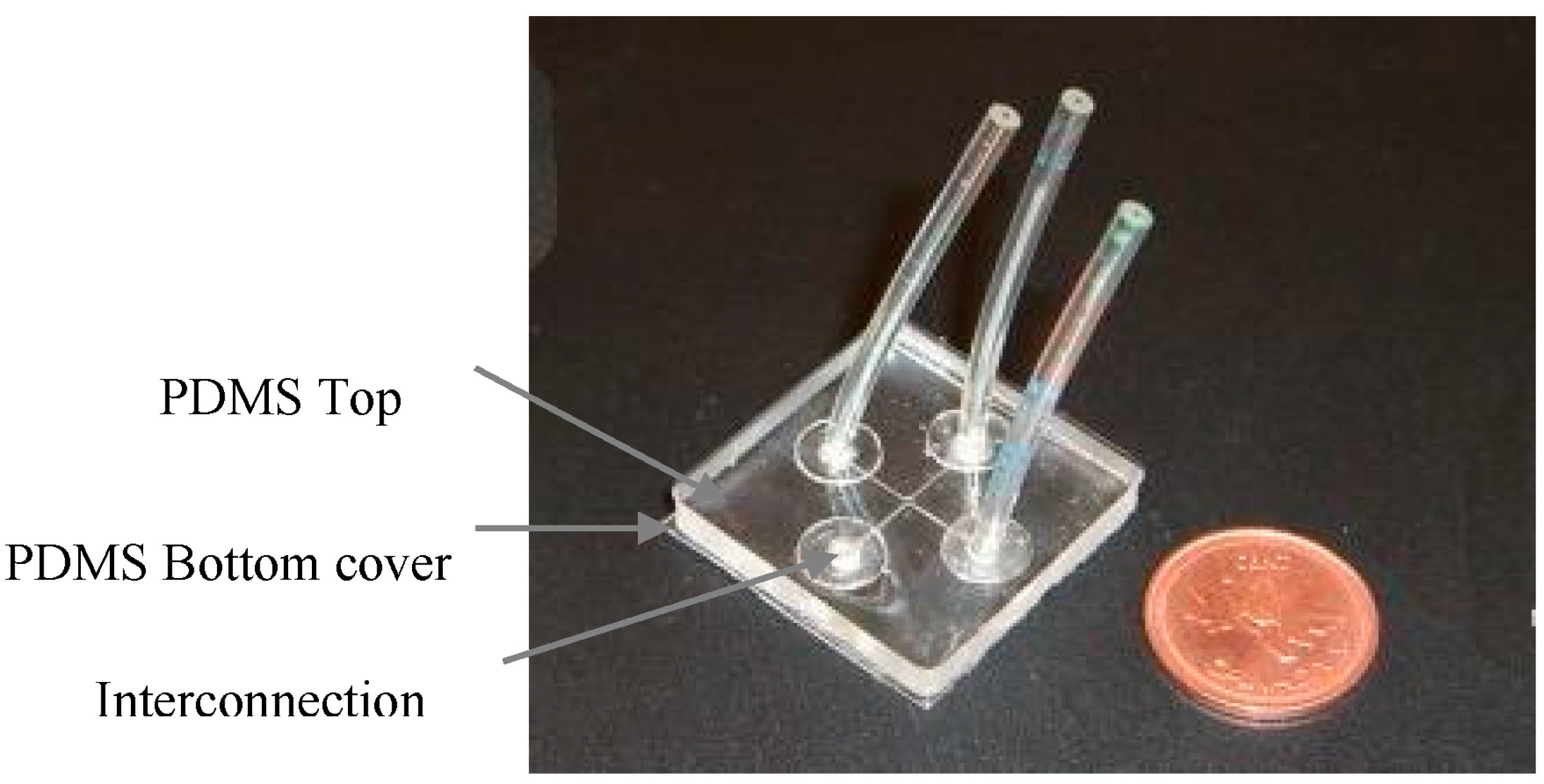
3. Design, Fabrication, Packaging and Integration

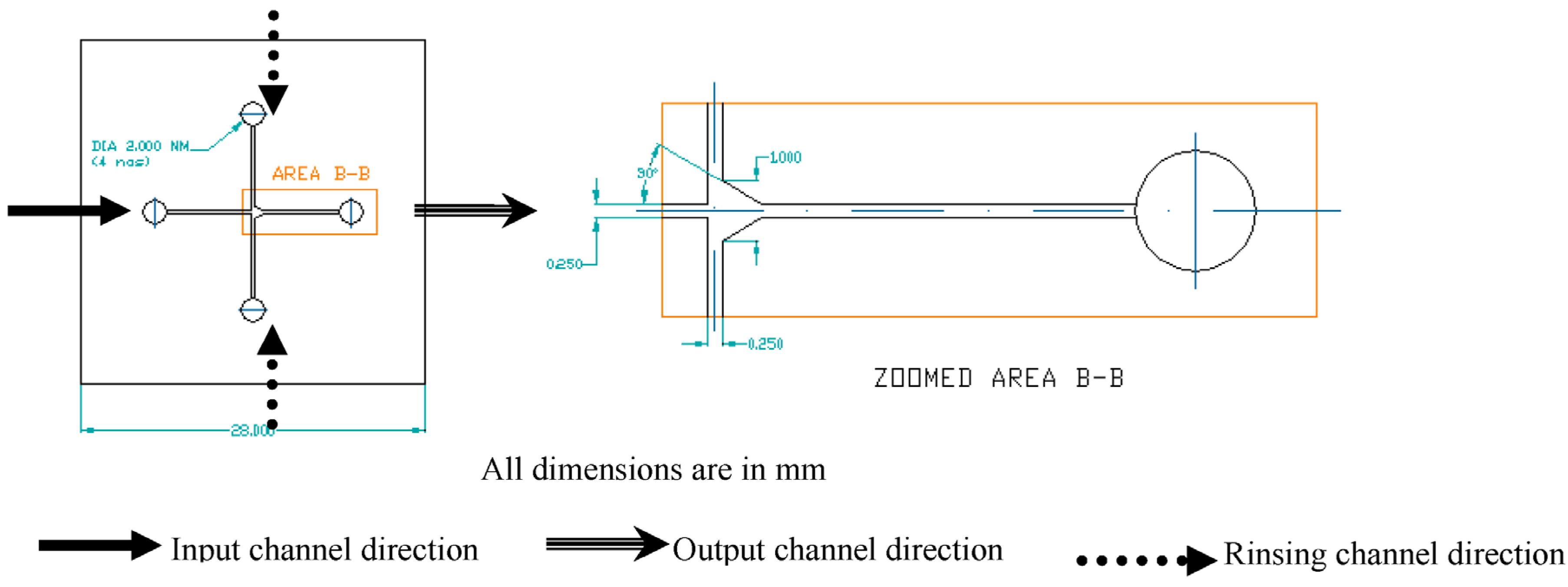
3.1. Design and Fabrication of Polymer based Microfluidic Chip

The re-usable polymer based microfluidic chip consists of an inlet port and two rinsing ports that intersect and lead to an outlet port. The intersecting region comprises of a micro-chamber, an integral part of the microfluidic chip essential for holding fluids. It also acts as a center of interest for bio interactions and optical detection. Design of micro-chambers must consider reusability of the micro-fluidic chip. Thus, it is also necessary to incorporate cleaning functions into the micro-chambers. The shape and size of the chamber is also a crucial factor for sensitivity of the sensor as the optical detection unit would be placed at the top of the chamber. Different combinations of chambers designs such as circular, elliptical, square and triangular shapes finally led to the design of triangular based micro-chamber. The flow simulations were carried for these shapes for both main and rinsing flow conditions. As the rinsing flow velocities are higher, there were recirculating flows formed introducing noise in the measurement for all geometries except triangular ones. Only the triangular chamber allows better rinsing properties with negligible slow zones and no reverse flow as compared to other designs. As the master template consisting of positive impression of the designed pattern was fabricated using CNC micromachining technique, it was also easier to fabricate a triangular based chamber. Hence, triangular geometry was selected for further design. CNC fabrication was found to be suitable for the required application in spite of possible high roughness of the mould. As the measurements are relative in terms of concentration, it was assumed that the scattering effect would be similar for all concentrations.
There are several optical detection techniques that are commonly used in microfluidic devices that use OLEDs as the illumination source. Fluorescence detection has gained some attention, as the extent of its efficiency does not depend on the optical path length. In spite of different kinds of detection techniques being used for qualitative and quantitative analysis of the sample, laser induced fluorescent technique will be an easier optical detection technique for microchip applications using OLEDs [29,30]. An increase in light path length through medium increases the colorimetric reading to a particular limit. These limits are decided by designing suitable sectional geometry of the reaction chamber (detection area) and the depth of microfluidic channel. While designing the sectional area of the reaction chamber, it should be noted that the area should be larger than the size of the detector. An increase in width of the chamber is a factor of fluorescent efficiency, as a large amount of fluorescence signal could be collected from the detectable area of the reaction chamber. While designing the depth of the microfluidic channel, it must be noted that the principle of detection is by fluorescence method wherein the detected signal is proportional to the concentration of antibody-antigen that is immobilized onto the microfluidic chamber. Thus, an increase in the channel depth after a particular limit does not signify an increase in the detection efficiency. Moreover, increasing the depth would result in an increase in fluid velocity and hence an increase in Reynolds number. This could harm the immobilized antigen-antibody layer and could unknowingly rinse out weakly bound antibody-antigen. In our fabricated device, the width and depth of the channels were designed to be 250 μm each. Suitable rinsing conditions with Phosphate buffer solution (PBS) and cleaning conditions with Isopropyl Alcohol (IPA) were determined accordingly and followed throughout the set of experiments. Rinsing and cleaning conditions are mentioned and paraphrased later in the bio-optical testing section. The size of the reaction chamber and other dimensions of the master template are designed as shown in Figure 1.
Figure 1. Features and dimensions of a master mold used for PDMS (polydimethylsiloxane) microfluidic chip.
Micromachines 06 01406 g001
The elastomer proposed for the fabrication is Polydimethylsiloaxane (PDMS) commercially named as Sylgard 184 (Dow Corning Corporation). PDMS pre-polymer and curing agent are poured into a Petri dish in the ratio 10:1 and mixed well for about 5 min. The mixture was then placed in a desiccators/vacuum pump setup until all the trapped air bubbles escape out. PDMS mixture was then poured into metal mastermold. The PDMS pre-polymer conforms to the shape of the master template and replicates the features of the mold. The mold was then carefully placed inside an oven and cured at 75 °C for 90 min. It was then carefully removed out using metal tongs and set to cool. Cured PDMS was peeled out gently from the mold.
Suitable interconnection and packaging techniques are essential to make an efficient and leak-proof microfluidic device. The cured open PDMS chip is then connected to the external world using tubes. This makes the top part of the microfluidic chip with channels and chamber embedded within it.
The top part of PDMS is then irreversibly bonded to an already fabricated 100 μm thick flat PDMS sheet using a polymer based adhesive. PDMS and similar siloxane polymers have a relatively low curing temperature, thus they are the most common adhesive bonding materials for microfluidic devices. Figure 2 shows the packaged microfluidic chip ready for integration to OLED source and optical detector.
Leakage is one of the most common post-packaging problems. This may arise due to one or many factors such as, not choosing a proper bonding methodology, uneven bonding between top and the bottom PDMS layers, uneven thickness of adhesive, interconnective clearance between the tube and the chip. Hence, testing of the packaged chip is essential before proceeding with the experiments. Leakage test was performed by passing a low viscous liquid. Isopropyl alcohol (Sigma Aldrich, Oakville, ON, Canada) was selected as fluid to check leakage. Since it is a low viscous chemical, any possibility of leaking can be easily seen by carefully observing the interfacial areas and interconnecting areas of the microfluidic chip. Initially rinsing ports were closed using metal connectors and IPA was pumped at 21 μL/min for 5 min using Gilson Minipuls two channel head Peristaltic Pump. This would create enough pressure within the channels and rinsing ports for it burst out from any weak interconnection. Fluidic chip’s interfacing areas between the top and bottom layers are carefully examined by using an Olympus BX 60MF5 DIC bright field microscope scaled to 20× magnification. Later, inlet port was closed and IPA was pumped through the rinsing ports to the outlet port by following the same pumping parameters and checked for leakage. Careful observations of interfacing surfaces and interconnecting places led to the conclusion that the fabricated chip is 100% leak proof and thus could be undoubtedly used for bio-optical testing.
Figure 2. Fabricated and packaged polymer based microfluidic chip.
Micromachines 06 01406 g002

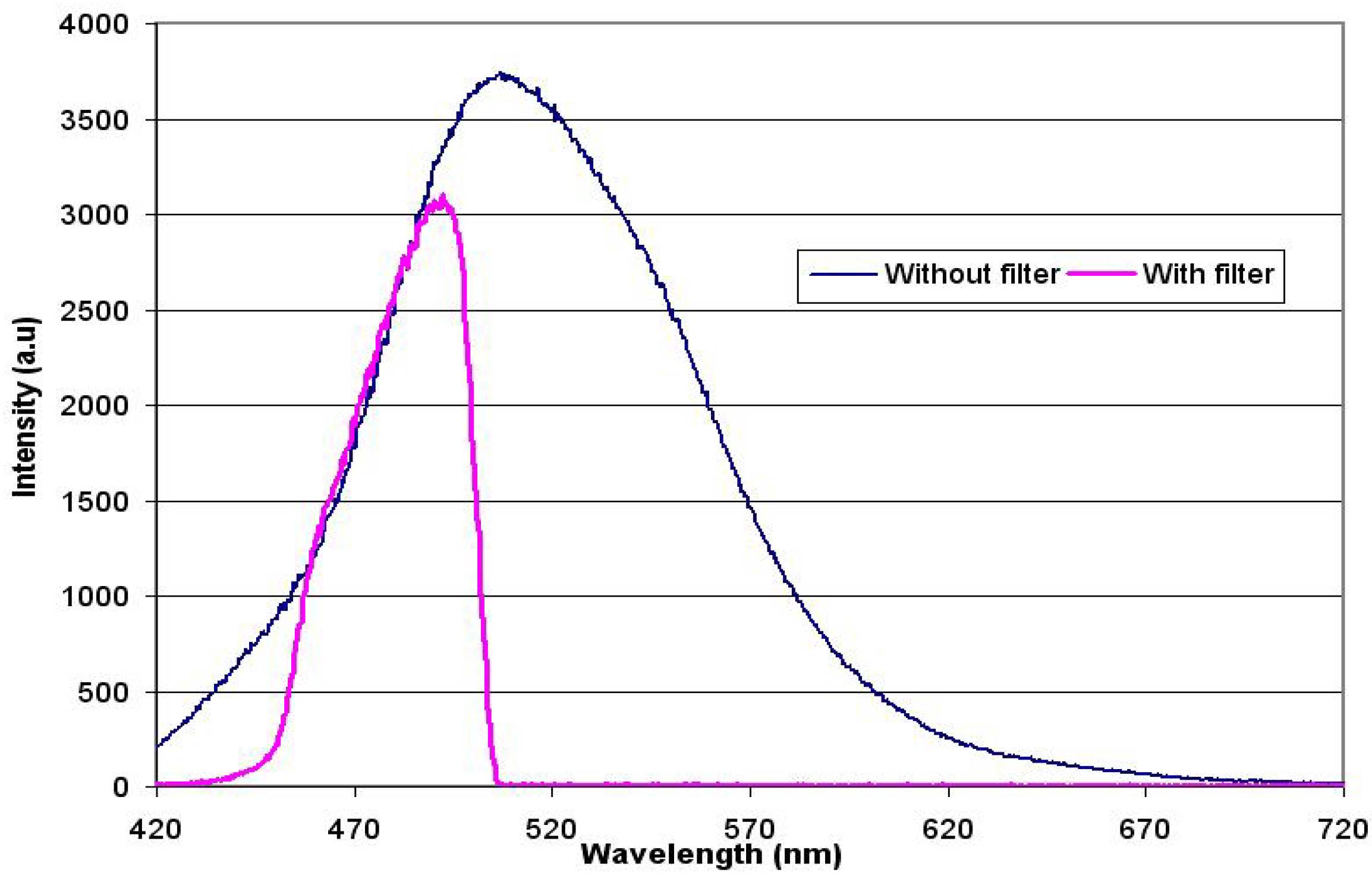
3.2. Design and Fabrication of OLED Chip as Excitation Source

One of the objectives of this paper is to demonstrate that it is possible to use a low cost OLED in order to build a biosensing platform. In order to do so, we used AlQ3, which is one of the more standard and low cost emitting materials for OLEDs’ fabrication. It can be shown that even though the maximum emittance of AlQ3 is situated in the green emission at around 507 nm, it can be used in conjunction with a fluorescence dye which excitation and emission peaks are situated at 495 and 519 nm, respectively. This can be done by taking advantage of the broad emission of an OLED and using an appropriate filter in order to cut wavelengths above 500 nm. OLEDs were fabricated on commercial ITO‑coated glass substrates (Colorado Concept Coatings LCC, 20 Ω/sq., 120–160 nm). ITO was first lithographically patterned, chemically cleaned and treated by oxygen plasma before loading into the vacuum chamber for organic material evaporation. The organic stack structure consists of 20 nm copper phthalocyanine (CuPc) hole injection and a buffer layer, a 50 nm 4,4′‑bis[N‑(1‑naphthyl)‑N‑phenyl-amino] biphenyl (α‑NPD) hole transport layer and a 50 nm tris‑(8‑hydroxyquinoline) aluminum (Alq3) electron transport and emissive layer. All the organic layers were deposited at deposition rates ranging from 0.2–0.3 nm·s−1 in a thermal evaporator with a base pressure of 2 × 10⁻⁶ Torr. The cathode was made by evaporating 1 nm of lithium fluoride and 100 nm of aluminum immediately followed by an organic layer deposition (i.e., without braking vacuum). OLED devices were removed from the evaporator and transferred into a glove box. They are then encapsulated by glass cover which is attached at the back of the device using UV sensitive epoxy. Glass cover prevents the device from exposure to moisture and hence enhances its life. Figure 3 shows the design layout of the fabricated OLED chip.
Figure 3. Design layout of organic light emitting diode (OLED) chip.
Micromachines 06 01406 g003

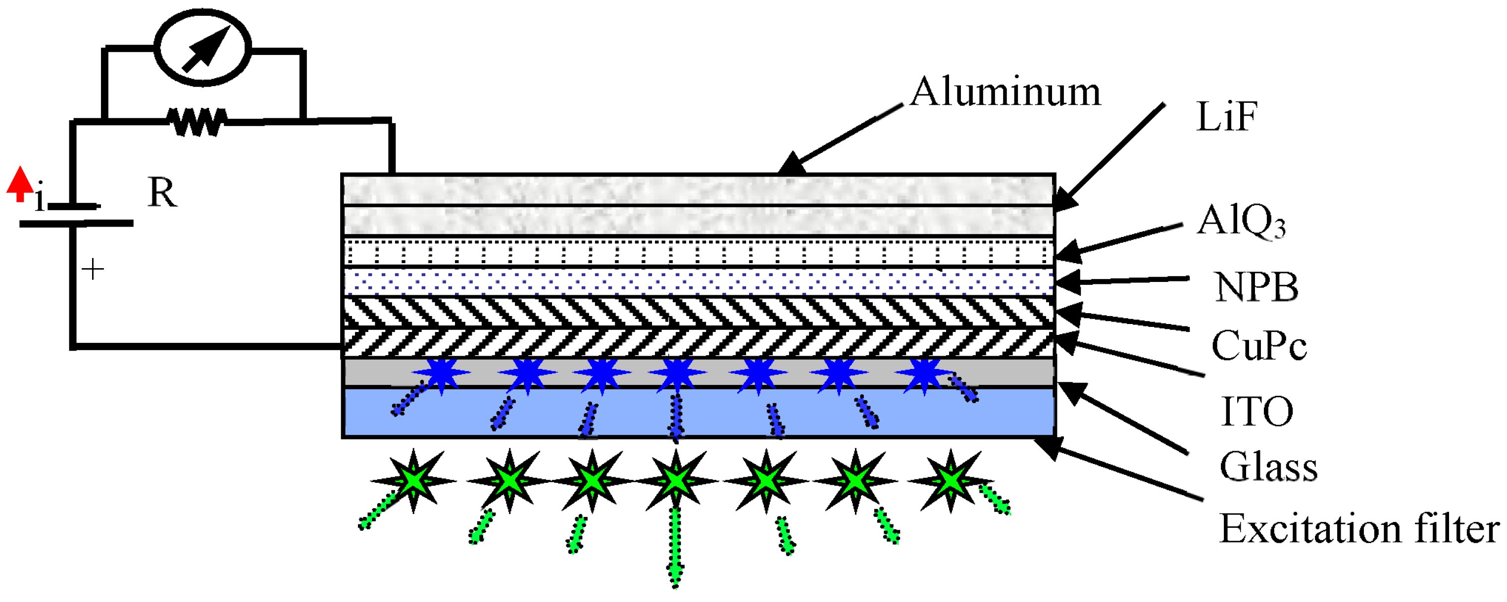
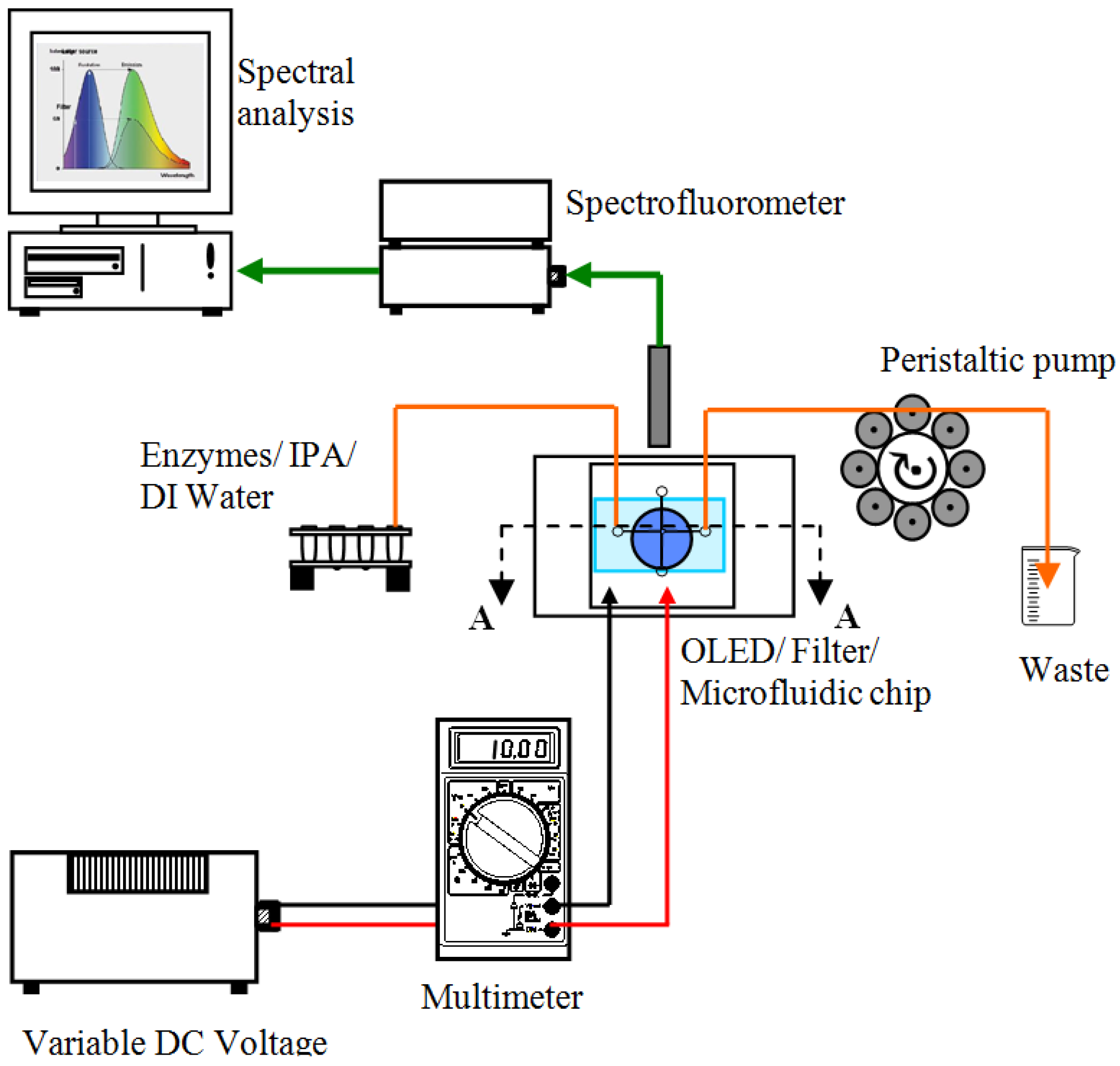
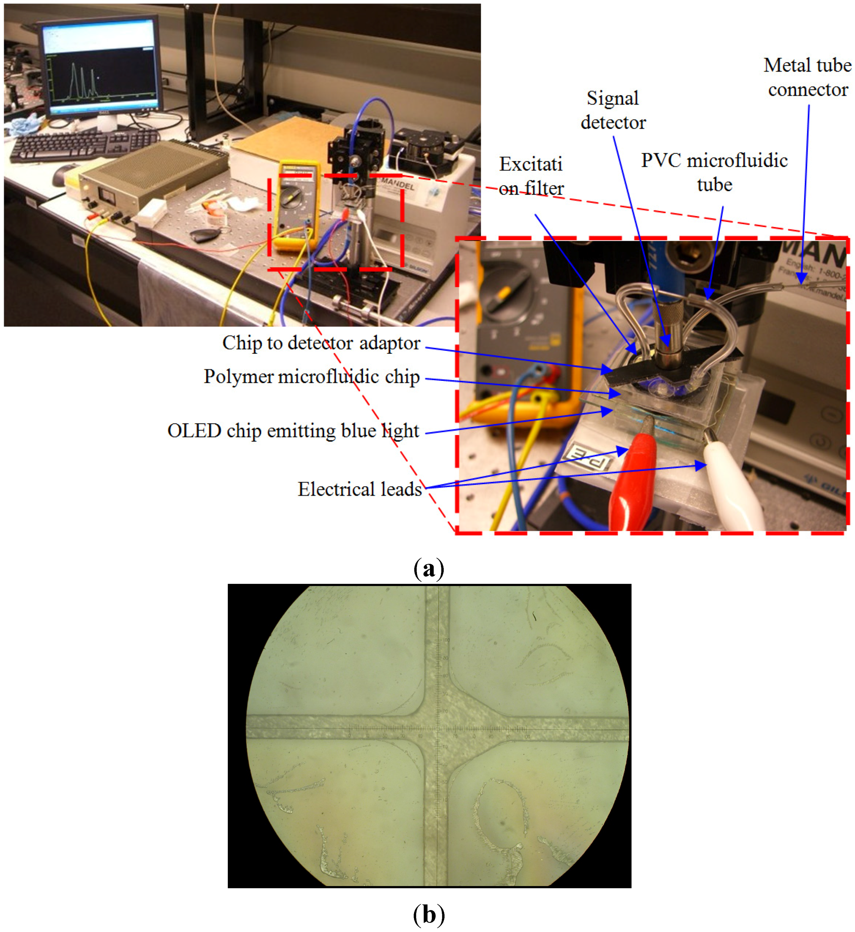
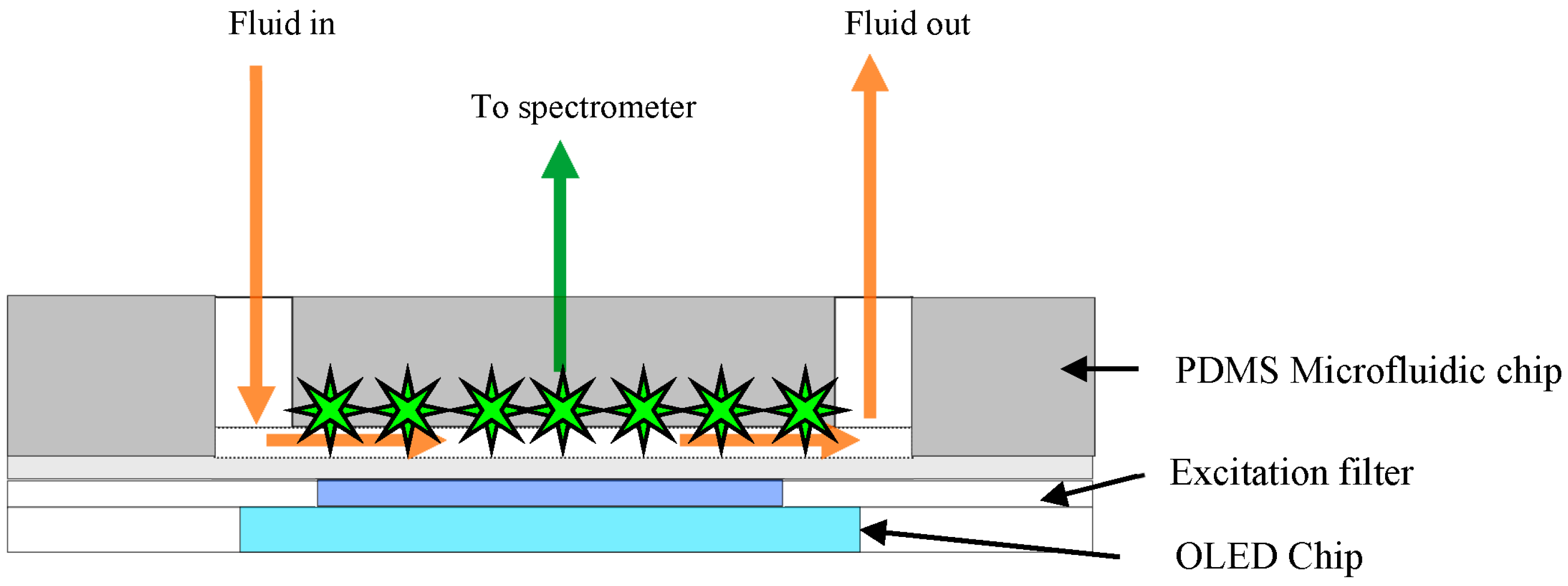
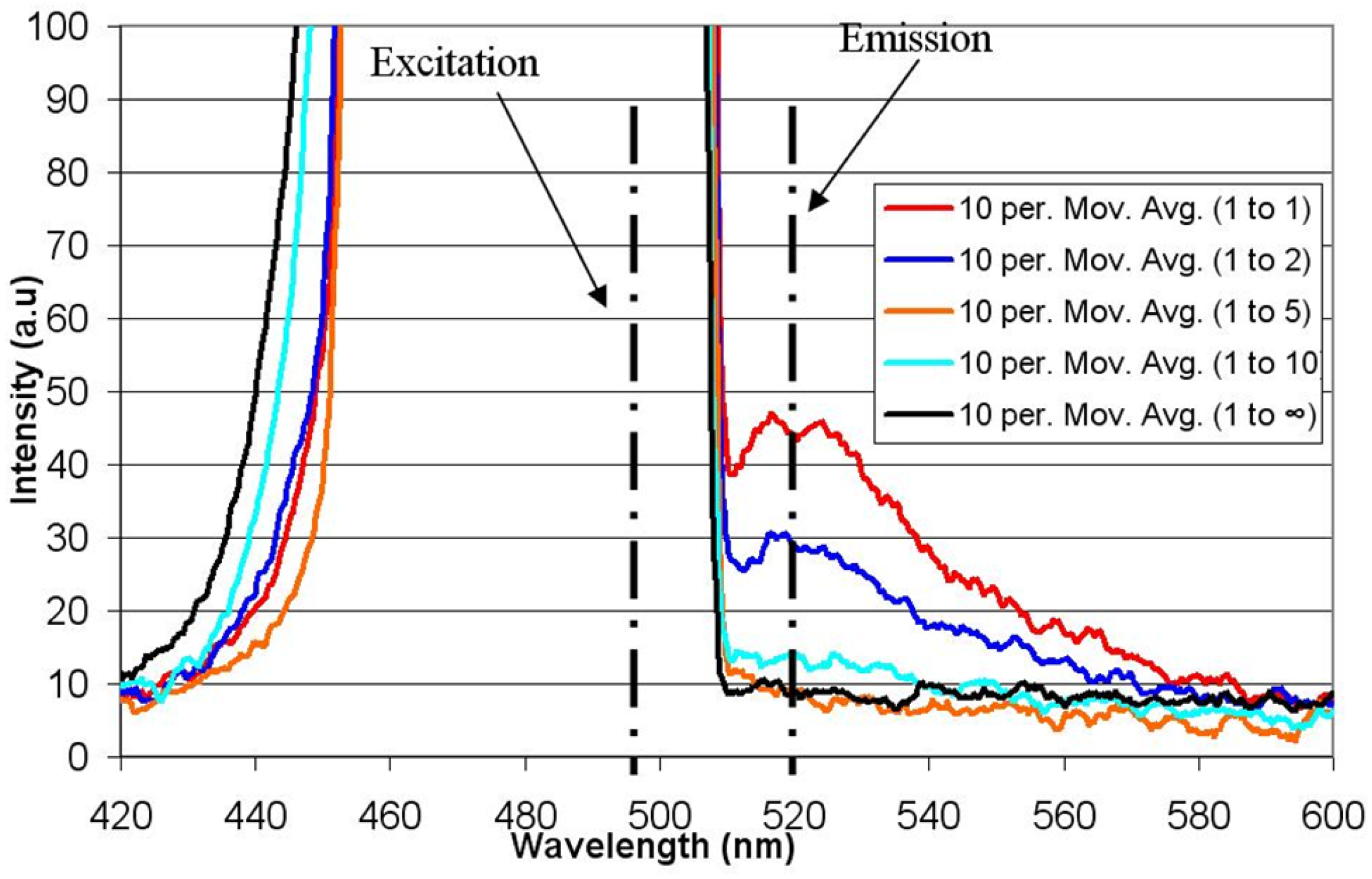
3.3. Bio-Organic Optical Integration and Detection System

Integrated bio-sensing system was set up by sandwiching a fabricated polymer based microfluidic chip between the OLED source at the bottom and the detection system at the top. Since the Stoke’s shift of the fluorescence species in the present work is about 24 nm, it is essential to narrow down the excitation wavelength band width to 10 nm so as to avoid interference of excitation intensity with the emitted signal. It was found that the full width at half maximum of OLED spectrum for a DC input voltage of 9 V to be around 80 nm with a peak at 507 nm. Since the characteristic excitation and emission peaks of the fluorescence dye used in the experiments was 495 and 519 nm, respectively, it was essential to select an excitation filter that would block noisy signals near the emission wavelength range. A high transmission sharp cutoff filter with band pass range between 460 and 500 nm from Iridian Spectral Technologies (Ottawa, ON, Canada), was chosen as an excitation filter and was placed between the OLED source and microfluidic chip. It was also observed as seen in Figure 4 that the excitation filter is efficient enough to transmit around 90% of the signal at a peak of 494 nm. Microfluidic chip with OLED source and excitation filter was mounted on a micro-positioner so that the position of the chip with respect to the output fiber could be easily adjusted. SMA fiber with a core diameter of 50 μm was connected inline to microfluidic chip by an adapter to capture the fluorescence signal. The fiber was connected to an Ocean Optics USB2000 Plug-and-Play Spectrometer at the other end. Figure 5 presents a schematic illustration of the OLED source-excitation filter-microfluidic chip-detector arrangement. The output signal was detected with Ocean Optics OOIBase32 Spectrometer interfaced to the computer. Using moving average data smoothing technique, peak detected signal and minimum concentration of the sample needed for detection were estimated.
Figure 4. OLED excitation with and without filter.
Micromachines 06 01406 g004
Figure 5. OLED source-filter-chip-detector setup.
Micromachines 06 01406 g005

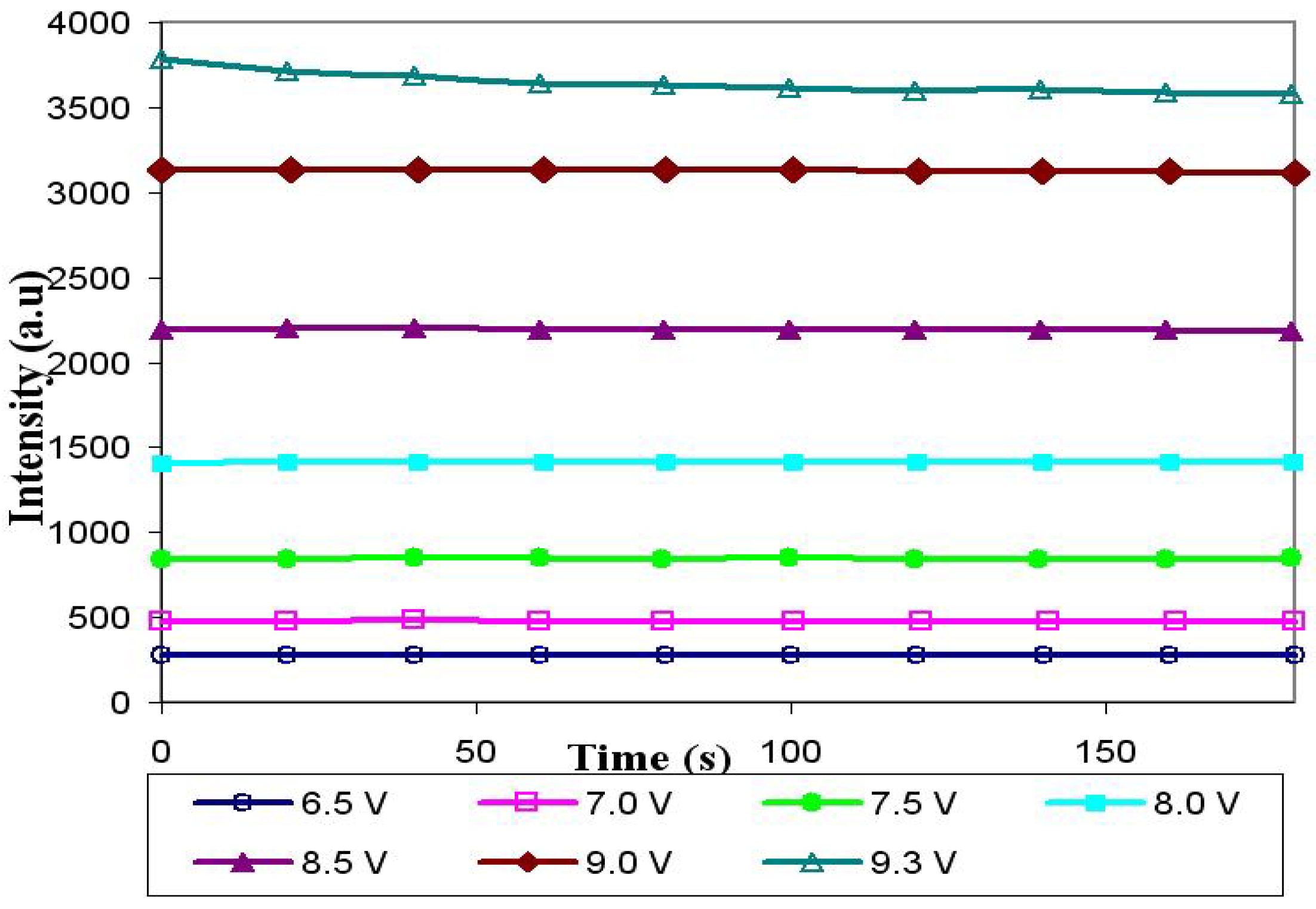
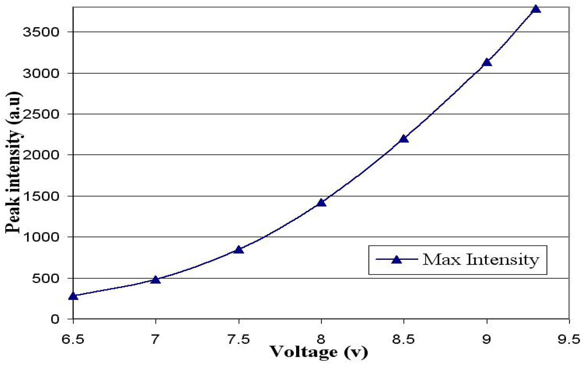
4. Stability of OLED Emission at Different Voltages

Determining the stability of the OLED source for a specific time interval is extremely important to determine the safe and consistent input voltage for the source. A steady DC voltage is required to excite the source such that the source must emit a prolonged stable light intensity without compromising for sensitivity of the sensor. OLED source was excited at different voltages. The power supply ranged from 6.5 to 9.5 V and the stability of the OLED emission intensity was recorded at regular intervals of 180 s. Figure 6 illustrates a comparison of stability of peak intensity being excited by OLED source at different voltages. It was found that an input DC voltage of 9.0 V was most favorable as the intensity was constant throughout the time interval and the emitted power was high enough to excite the fluorescence tagged enzymes with the microfluidic chip. Further, it was also observed that intensity follows a negative dip for 9.5 V input voltage. It could be concluded that operating voltage of the OLED source must be less than or equal to 9.0 V as higher voltages would reduce the life of the source. The presented OLED can be operated with a battery for the short periods of illumination needed to proceed to the measurement. In this way, the voltage could be kept bellow 9.3 V ensuring that there will be no degradation in the intensity emission of the OLED. Figure 7 also shows that the peak intensity increases drastically for higher voltages; hence a very small drop in voltage would affect the sensitivity of the sensor. Thus, 9.0 V DC voltage source was chosen as the operating voltage to excite the OLED source throughout the experiments. The operation of the OLED at a voltage around or less than 9 V will result in negligible temperature increase. This is illustrated on Figure 6 where it is shown that there is no variation of intensity during operation for more than 2 min. Similarly, one would expect negligible change in peak wavelength.
Figure 6. Stability of OLED excitation at different voltages for a peak wavelength of 496 nm.
Micromachines 06 01406 g006
Figure 7. Variation of peak intensity of OLED emission for different voltages at 496 nm wavelength.
Micromachines 06 01406 g007

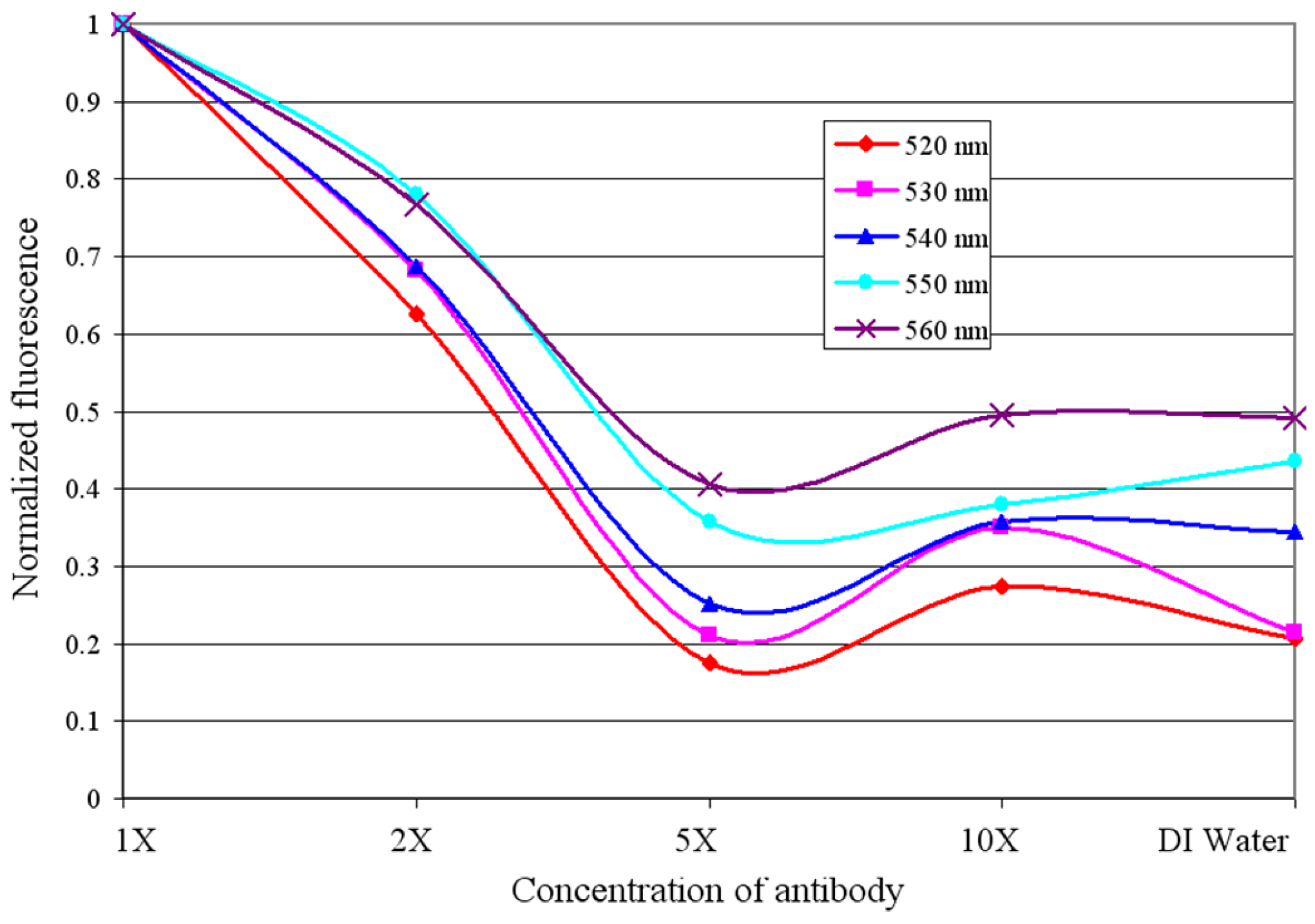
5. Bio-Optical Testing on Microfluidic Chip

5.1. Selection and Preparation of Enzymes

To demonstrate the practical application and limit of sensitivity of the biosensor based on OLED source excitation, laser induced fluorescence tests were carried out for different concentrations of secondary antibody. A vial of Donkey anti–sheep IgG conjugates were purchased from Invitrogen-Molecular Probes (Ottawa, ON, Canada). The sample contains 2 mg/mL solution in 0.1 M sodium phosphate, 0.1 M NaCl, pH 7.5, containing 2–5 mM sodium azide and tagged to Alexafluor 488 fluorescence dye. Alexafluor 488 has an adsorption peak of 495 nm and an emission peak of 519 nm.
Phosphate buffer solution (PBS) is used as a buffer solution and a diluting agent. To start with, stock solution of working concentration of 2 μg/mL is prepared by diluting secondary antibody with PBS. The stock solution is taken as a standard for further diluting the sample. Four different concentrations of the sample were prepared: 1×, 2×, 5×, and 10×, by further diluting the stock with PBS. Isopropyl Alcohol (IPA) was used as a cleansing agent to rinse out sample from the microfluidic channels for subsequent sets of experiments. All these samples were stored undiluted at 4 °C and protected from light as per the Invitrogen-Molecular Probes storage instructions.
Figure 8 presents the schematic representation of the bio-optical fluorescence detection setup using OLED source. Gilson Minipuls two channel Peristaltic Pump was used from driving flow medium, water and IPA throughout the experiment. One of the tubes/channels was used to pump in antigen, antibody or PBS through inlet port and the other tube was connected to pump in IPA or water for the cleansing process. It was decided to pump in the sample by suction rather than by driving out because suction of fluid not only reduces the time taken to fill and rinse out the microfluidic chamber by 50% but also saves precious bio molecules.
Figure 8. Schematic representation of the bio-optical fluorescence detection setup using OLED source.
Micromachines 06 01406 g008
A variable DC voltage source was connected to the electrodes of the integrated OLED chip and voltage is measured using multimeter. Detected signal is collected by optical fiber which in turn is connected to a spectrometer interfaced to a computer. The testing setup is shown in Figure 9. The entire set of experiments was carried out in a dark environment to avoid optical noise from external sources. Isopropyl Alcohol (IPA) was used as a cleansing agent, with high velocity, to rinse out sample from the microfluidic channels for subsequent set of experiments. Due to this arrangement, the chip can be reused around three times.
Figure 9. (a) Schematic of bio-optical fluorescence detection setup using OLED source. (b) Close up of Triangular Chamber.
Micromachines 06 01406 g009

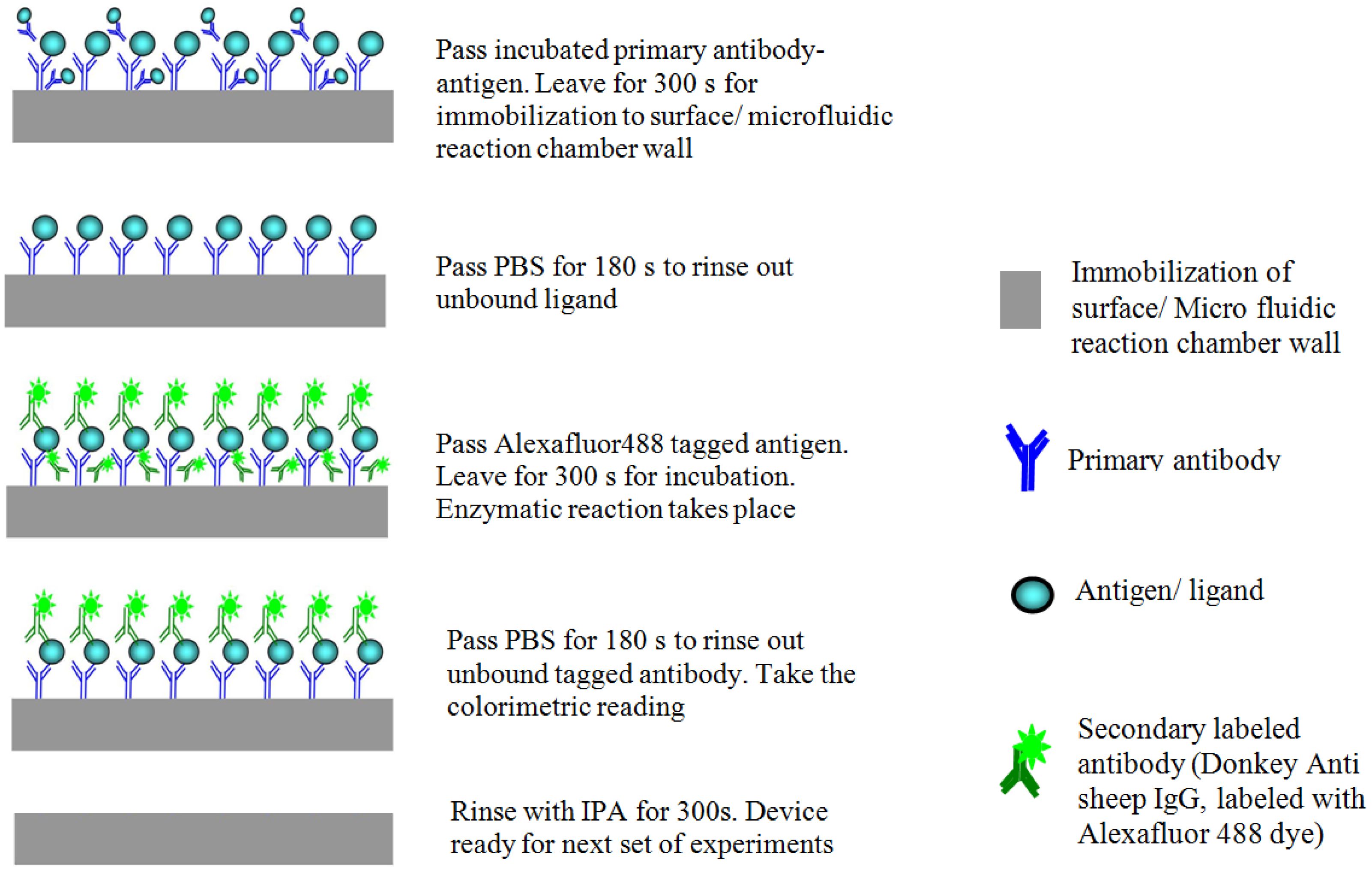
5.2. Bio-Optical Detection Methodology

Fluorescence based immunoassay is one of the simplest and most widely used biochemical tests that gives a qualitative and quantitative measure of the presence of known or unknown analyte (antigen in our case) within the biological liquid [9,22]. Detection is achieved by measuring the interaction of tagged antibodies with antigen in order to detect the presence and count of enzymes, peptides, viruses, antibodies and hormones, etc. This matched pair of primary and fluorescence tagged secondary antibodies is monoclonal in nature and has the unique characteristic to bind to a particular site (epitope) of antigen with high affinity. Thus, depending on a particular instance, the presence of antigen within the sample could be measured as a colorimetric signal of particular wavelength towards an induced excited wavelength. The intensity or voltage response given out by spectrophotometer (Ocean Optics, Model STS-VIS-S04627) or photodiode is then compared with calibrated standard plots which give the measure of the level of antigen present in the sample.
Bio testing with an integrated device was carried out for different concentrations of secondary antibody in order to establish the sensitivity, throughput and reliability. Our goal is to detect the minimum level concentration of fluorescing signal from the samples prepared. Firstly, the entire channel and chamber was cleaned by passing HCl (Sigma Aldrich) and deionized water (DI water) (1:10) and then with DI water mixed with 0.1% Tween 20 surfactant (Sigma Aldrich) for 15 min. Doing this not only ensures clean and uncontaminated chip for the experiments but also helps retain the hydrophilic nature of the channel.
The type of detection used here is called as sandwich type immunoassay process which is based on fluorescence detection of antigen that is sandwiched between two antibodies. Firstly, PBS was passed through inlet and rinsing ports at 1.00 rpm pump speed for 180 s to initiate the experiments. The primary antibody which is already incubated to one of the two epitopes of antigen is then pumped through inlet port at 0.50 rpm for 180 s. When the antigen is left undisturbed for 300 s, it immobilizes onto the biocompatible surface of the microfluidic reaction/mixing chamber. Unbound ligand is then removed by rinsing the chamber with PBS at 0.50 rpm pumps speed for 180 s. A 10× diluted secondary antibody conjugate which is tagged to a Alexafluor 488 is then pumped into the reaction chamber at 0.50 rpm for 180 s and kept undisturbed for 300 s for incubation. The incubation time allows the immobilized antigen to bind to the antibody with high affinity. Unbound antibody is then removed by rinsing the chamber with PBS at 0.50 rpm pumps speed for 180 s. This forms one-one-one-one interactive chain between primary antibody-antigen-secondary antibody-fluorophore. The interaction which is measured as emitted signal thus correlates with the measure of the number of secondary antibody which in turn is the measure of number of antigen. Hence, the emitted signal reading given as light intensity or voltage output is directly proportional to the amount of detected antigen. Such a way of interpreting results is known is densitometric analysis and is measured using an Ocean Optics spectrofluorometer. This method is of the heterogeneous immunoassay type as the process requires removal of unbound antibody or antigen from the reaction chamber after incubation and immobilization steps. Hence, the process is also known as the heterogeneous non-competitive immunoassay process. Figure 10 illustrates the process flow of the sandwich type immunoassay process for bio-optical detection of antigen tagged to various concentrations of Donkey anti-sheep IgG conjugates.
Once the fluorescence readings were recorded, the channel was flushed with IPA and the procedure was repeated with 5×, 2× and 1× concentrations of the fluorophore tagged secondary antibody. It should be noted that the flow speed for passing the bio analytes was always maintained at 0.50 rpm and pump speed for rinsing conditions was increased to 1.00 rpm. The optimized pump speeds were established as the most favorable flow rates which would give an optimum binding of enzymes to the microfluidic chamber and sufficient speed for flushing out the chamber and channels.
The obtained results on fluorescence detection of tagged Donkey anti-sheep IgG conjugates in the microfluidic channel using OLED excitation are given in Figure 11. The peak at 519 nm is the result of fluorescence emitted by the Alexafluor dyes due to excitation at 495 nm. The spectral response of the fluorescence testing was plotted as shown. It is seen that maximum emission is given out at 1× diluted (0.2 μg/mL) antibody Donkey anti-sheep IgG conjugates. Minimum emission peak is seen for 5× diluted antibody. Further, no significant emission is observed for the 10× diluted antibody. The fluorescence unit is normalized for different wavelengths with respect to the fluorescence observed at the highest concentration of the antibody. Since fluorescence is a function of emission intensity of the fluorophore, this relationship will be more useful to study the effect of surface immobilizing capacity against concentration and hence to detect minimum detection capacity or sensitivity of the biosensor. It can be clearly observed from Figure 12 that the normalized graphs at different wavelengths follow the same trend with a dip at 5× concentration and again a rise. The experimental details in Figure 11 and Figure 12 are the average of 10 samples. It could be inferred from the graph that the trend depicting the fluorescence intensity diverges after 5× concentration and hence is the minimum detectable concentration of the antibody.
Figure 10. Process flow of immunoassay fluorescence detection for bio-optical detection of antigen.
Micromachines 06 01406 g010
Figure 11. Fluorescence spectral response curve of Alexafluor 488-antibody with sheep IgG at 9 V (zoomed/moving average).
Micromachines 06 01406 g011
Figure 12. Comparison of normalized fluorescence for different concentration of antibody at various wavelengths.
Micromachines 06 01406 g012

6. Conclusions

In this work, a polymer based microfluidic platform and Organic LED were designed and developed in-house and were successfully externally hybrid integrated with an excitation filter and detector. The biosensing element was tested to detect anti-sheep IgG conjugates tagged to Alexafluor 488 using fluorescence based immunoassay method. The minimum detectable concentration of the antibody was also identified experimentally. The results show that OLEDs could be integrated to polymer based microfluidic platforms in future to establish a simple and cost effective biosensing element for rapid in-situ detection of enzymes and proteins.

Acknowledgments

The authors thank Sébastien Pigeon from OLA Display Corp. for the fabrication of Organic light emitting diode. The authors also thank NSERC and SRT (ENCS) for providing financial support for this work.

Author Contributions

Muthukumaran Packirisamy designed and conceptualized the project. Ricardo Izquierdo designed and supervised the OLED development. Ashwin Acharya carried out the fabrication and testing of the device. All authors contributed to the preparation and editing of the manuscript.

Conflicts of Interest

The authors declare no conflict of interest.

References

  1. Ahn, C.H.; Choi, J.; Beaucage, G. Disposable smart lab on a chip for point-of-care clinical diagnostics. Proc. IEEE 2004, 92, 154–173. [Google Scholar] [CrossRef]
  2. Allen, P.B.; Rodriguez, I.; Kuyper, C.L.; Lorenz, R.M.; Spicar-Mihalic, P.; Kuo, J.S.; Chiu, D.T. Selective Electroless and Electrolytic Deposition of Metal for Applications in Microfluidics:  Fabrication of a Microthermocouple. Anal. Chem. 2003, 75, 1578–1583. [Google Scholar] [CrossRef] [PubMed]
  3. Altendorf, E.; Zebert, D.; Holl, M.; Yager, P. Differential blood cell counts obtained using a microchannel based flow cytometer. In Proceedings of IEEE International Conference on Solid-State Sensors and Actuators (TRANSDUCERS’97), Chicago, IL, USA, 16–19 June 1997; pp. 531–534.
  4. Bashir, R. State-of-the-art in detection, opportunities and prospects. Adv. Drug Deliv. Rev. 2004, 56, 1565–1586. [Google Scholar] [CrossRef] [PubMed]
  5. Bessoth, F.G.; Naji, O.P.; Eijkel, J.C.T.; Manz, A. Towards an on-chip gas chromatograph: The development of a gas injector and a dc plasma emission detector. J. Anal. At. Spectrom. 2002, 17, 794–799. [Google Scholar] [CrossRef]
  6. Brehmer, M.; Conrad, L.; Funk, L. New developments in soft lithography. J. Dispers. Sci. Technol. 2003, 24, 291–304. [Google Scholar] [CrossRef]
  7. Camou, S.; Kitamura, M.; Arakawa, Y.; Fuji, T. Integration of OLED light source and optical fibers on a PDMS based microfluidic device for on-chip fluorescence detection. In Proceedings of 7th International Conference on Miniaturized Chemical and Biochemical Analysis Systems, Squaw Valley, CA, USA, 5–9 October 2003; pp. 383–386.
  8. Chabinyc, M.L.; Chiu, D.T.; McDonald, J.C. An integrated fluorescence detection system in poly(dimethylsiloxane) for microfluidic applications. Anal. Chem. 2001, 73, 4491–4498. [Google Scholar] [CrossRef] [PubMed]
  9. Choi, J.W.; Oh, K.W.; Thomas, J.H. An integrated microfluidic biochemical detection system for protein analysis with magnetic bead-based sampling capabilities. Lab Chip 2002, 2, 27–30. [Google Scholar] [CrossRef] [PubMed]
  10. Coté, G.L.; Lec, R.M.; Pishko, M.V. Emerging biomedical sensing technologies and their applications. IEEE Sens. J. 2003, 3, 251–266. [Google Scholar] [CrossRef]
  11. Pinto, V.C.; Sousa, P.J.; Cardoso, V.F.; Minas, G. Optimized SU-8 Processing for Low-Cost Microstructures Fabrication without Cleanroom Facilities. Micromachines 2014, 5, 738–755. [Google Scholar] [CrossRef] [Green Version]
  12. Effenhauser, C.S.; Bruin, G.J.M.; Paulus, A.; Ehrat, M. Integrated capillary electrophoresis on flexible silicone microdevices: Analysis of DNA restriction fragments and detection of single DNA molecules on microchips. Anal. Chem. 1997, 69, 3451–3457. [Google Scholar] [CrossRef] [PubMed]
  13. Erickson, D.; Li, D. Integrated microfluidic devices. Anal. Chim. Acta 2004, 507, 11–26. [Google Scholar] [CrossRef]
  14. Fintschenko, Y.; Wilson, G.S. Flow injection immunoassays: A review. Microchim. Acta 1998, 129, 7–18. [Google Scholar] [CrossRef]
  15. Hofmann, O.; Wang, X.; deMello, J.C.; Bradley, D.D.; deMello, A.J. Towards microalbuminuria determination on a disposable diagnostic microchip with integrated fluorescence detection based on thin-film organic light emitting diodes. Lab Chip 2005, 5, 863–868. [Google Scholar] [CrossRef] [PubMed]
  16. Jorgensen, A.M.; Mogensen, K.B.; Kutter, J.P.; Geschke, O. A biochemical microdevice with an integrated chemiluminescence detector. Sens. Actuators B Chem. 2003, 90, 15–21. [Google Scholar] [CrossRef]
  17. Lapos, J.A.; Manica, D.P.; Ewing, A.G. Dual fluorescence and electrochemical detection on an electrophoresis microchip. Anal. Chem. 2002, 74, 3348–3353. [Google Scholar] [CrossRef] [PubMed]
  18. Laser, D.; Santiago, J. A review of micropumps. J. Micromech. Microeng. 2004, 14, 35–64. [Google Scholar] [CrossRef]
  19. Li, J.; Thibault, P.; Bings, N.H. Integration of microfabricated devices to capillary electrophoresis-electrospray mass spectrometry using a low dead volume connection: Application to rapid analyses of proteolytic digests. Anal. Chem. 1999, 71, 3036–3045. [Google Scholar] [CrossRef] [PubMed]
  20. Liang, Z.; Chiem, N.; Ocvirk, G.; Tang, T.; Fluri, K.; Harrison, D.J. Microfabrication of a planar absorbance and fluorescence cell for integrated capillary electrophoresis devices. Anal. Chem. 1996, 68, 1040–1046. [Google Scholar] [CrossRef]
  21. Sia, S.K.; Whitesides, G.M. Microfluidic devices fabricated in poly(dimethylsiloxane) for biological studies. Electrophoresis 2003, 24, 3563–3576. [Google Scholar] [CrossRef] [PubMed]
  22. Linder, V.; Verpoorte, E.; Thormann, W.; de Rooij, N.F.; Sigrist, H. Surface biopassivation of replicated poly(dimethylsiloxane) microfluidic channels and application to heterogeneous immunoreaction with on-chip fluorescence detection. Anal. Chem. 2001, 73, 4181–4189. [Google Scholar] [CrossRef] [PubMed]
  23. Massin, C.; Vincent, F.; Homsy, A. Planar microcoil-based microfluidic NMR probes. J. Magn. Resonance 2003, 164, 242–255. [Google Scholar] [CrossRef]
  24. McDonald, J.C.; Whitesides, G.M. Poly (dimethylsiloxane) as a material for fabricating microfluidic devices. Acc. Chem. Res. 2002, 35, 491–499. [Google Scholar] [CrossRef] [PubMed]
  25. Zmija, J.; Malachowski, M.J. Organic light emitting diodes operation and application in displays. Arch. Mater. Sci. Eng. 2009, 40, 5–12. [Google Scholar]
  26. Woolley, A.T.; Lao, K.; Glazer, A.N.; Mathies, R.A. Capillary electrophoresis chips with integrated electrochemical detection. Anal. Chem. 1998, 70, 684–688. [Google Scholar] [CrossRef] [PubMed]
  27. Xia, Y.; Whitesides, G.M. Soft lithography. Annu. Rev. Mater. Sci. 1998, 28, 153–184. [Google Scholar] [CrossRef]
  28. Yao, B.; Luo, G.; Wang, L. A microfluidic device using a green organic light emitting diode as an integrated excitation source. Lab Chip 2005, 5, 1041–1047. [Google Scholar] [CrossRef] [PubMed]
  29. Verpoorte, E.; De Rooij, N. Microfluidics meets MEMS. Proc. IEEE 2003, 91, 930–953. [Google Scholar] [CrossRef]
  30. Weigl, B.H.; Bardell, R.L.; Cabrera, C.R. Lab-on-a-chip for drug development. Adv. Drug Deliv. Rev. 2003, 55, 349–377. [Google Scholar] [CrossRef]

