
Fabrication of 2-D Capacitive Micromachined Ultrasonic Transducer (CMUT) Array through Silicon Wafer Bonding

 , , , ,
Abstract
:1. Introduction
2. Materials and Methods
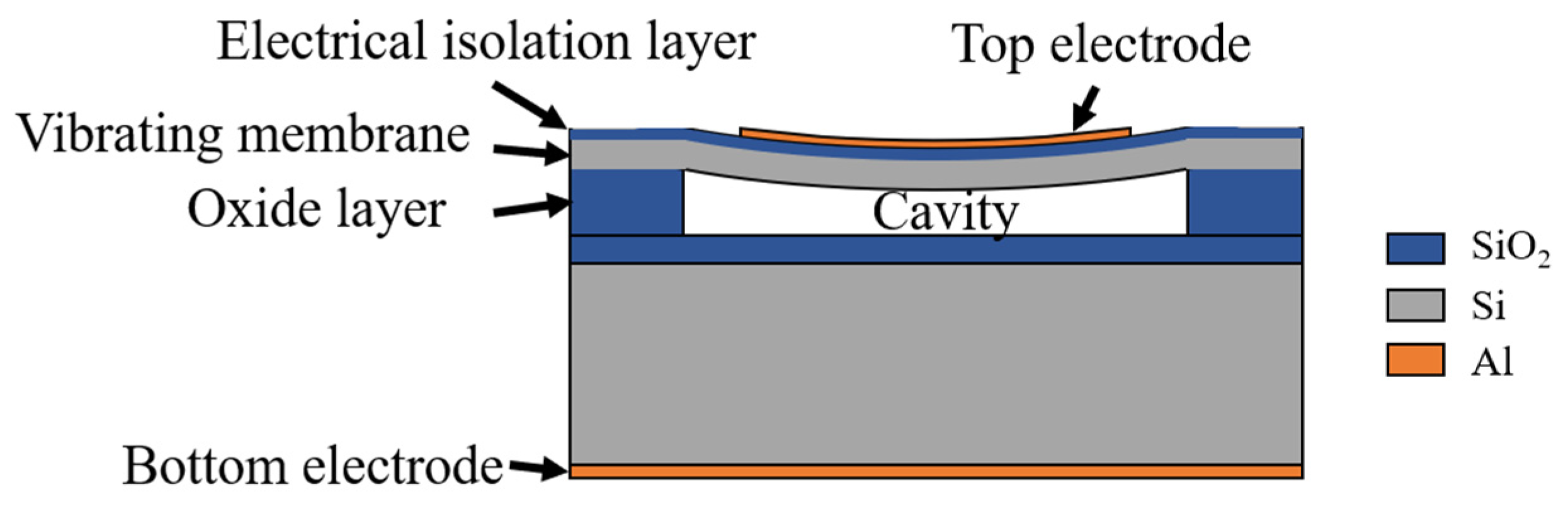
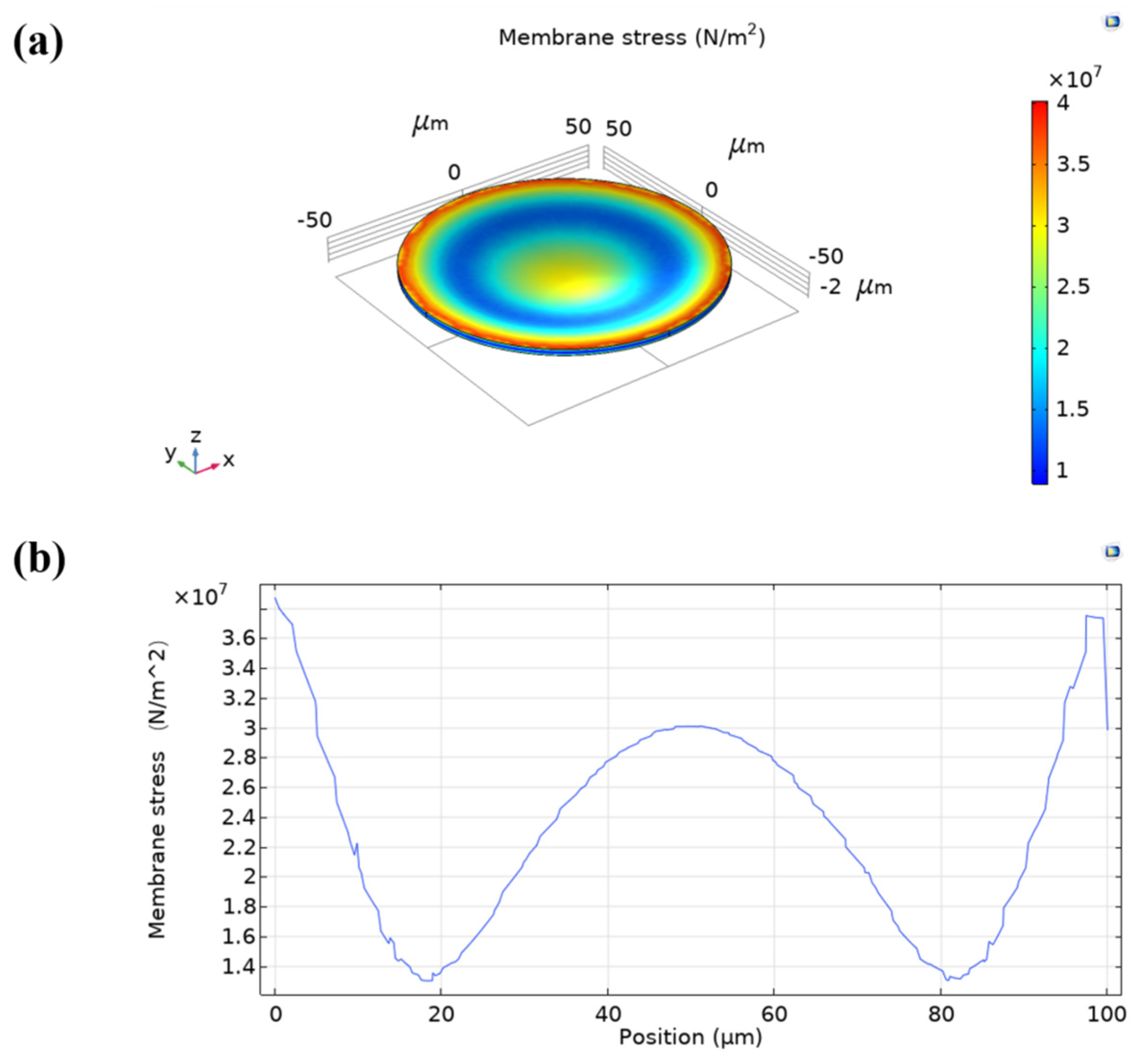
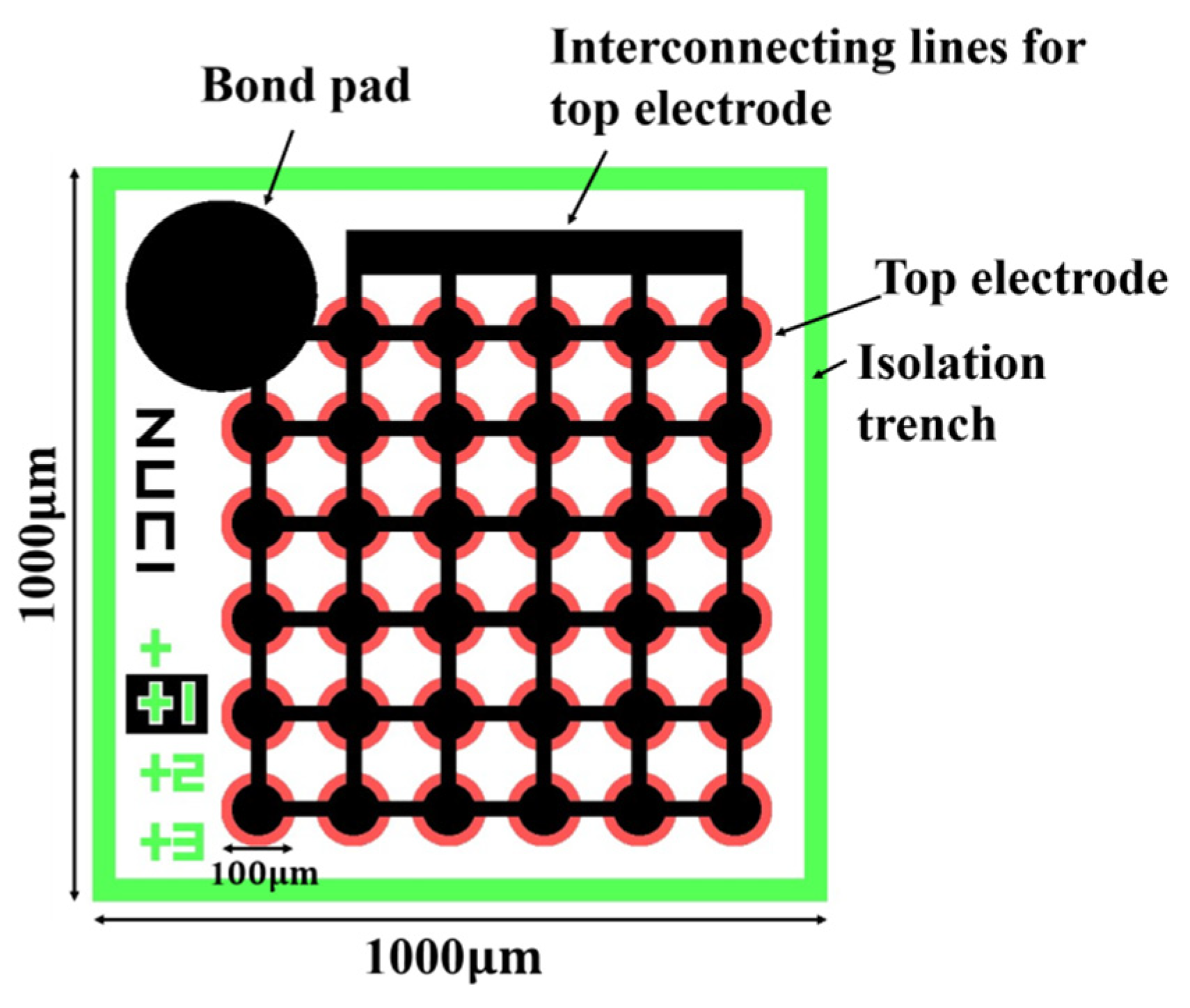
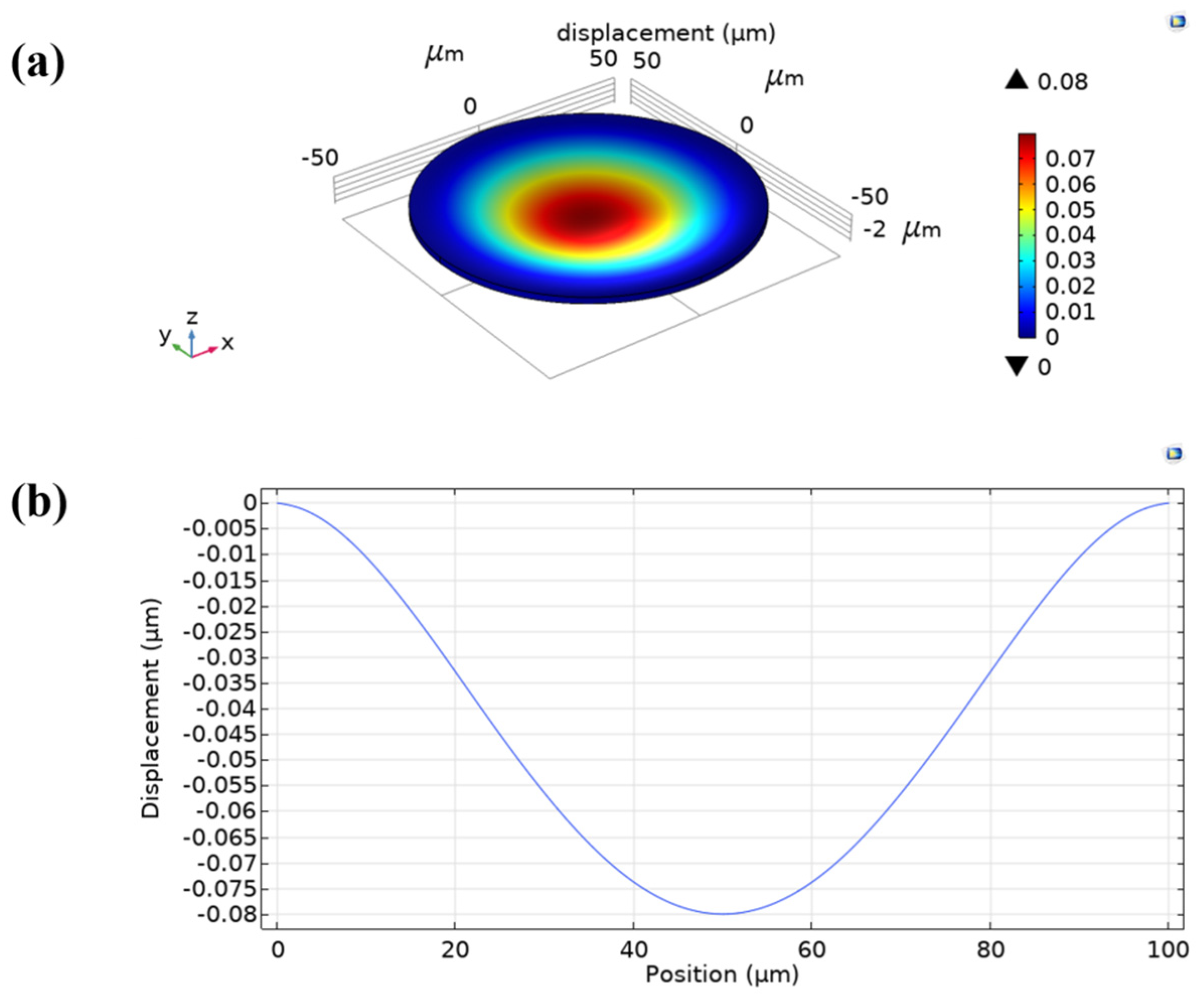
2.1. Transducer Structure
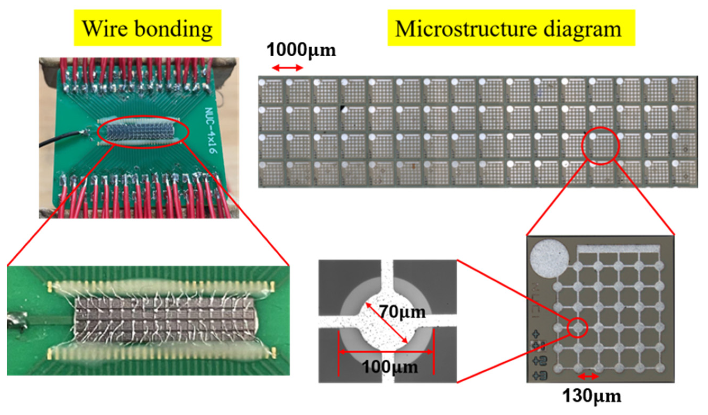
2.2. CMUT Array Fabrication
2.2.1. Wafer Preparation
2.2.2. Silicon Wafer Bonding
2.2.3. Micromachining
2.2.4. Isolation Groove Etching, Electrical Isolation, and Metal Graphics
2.2.5. Metal Wire Bonding
3. Results
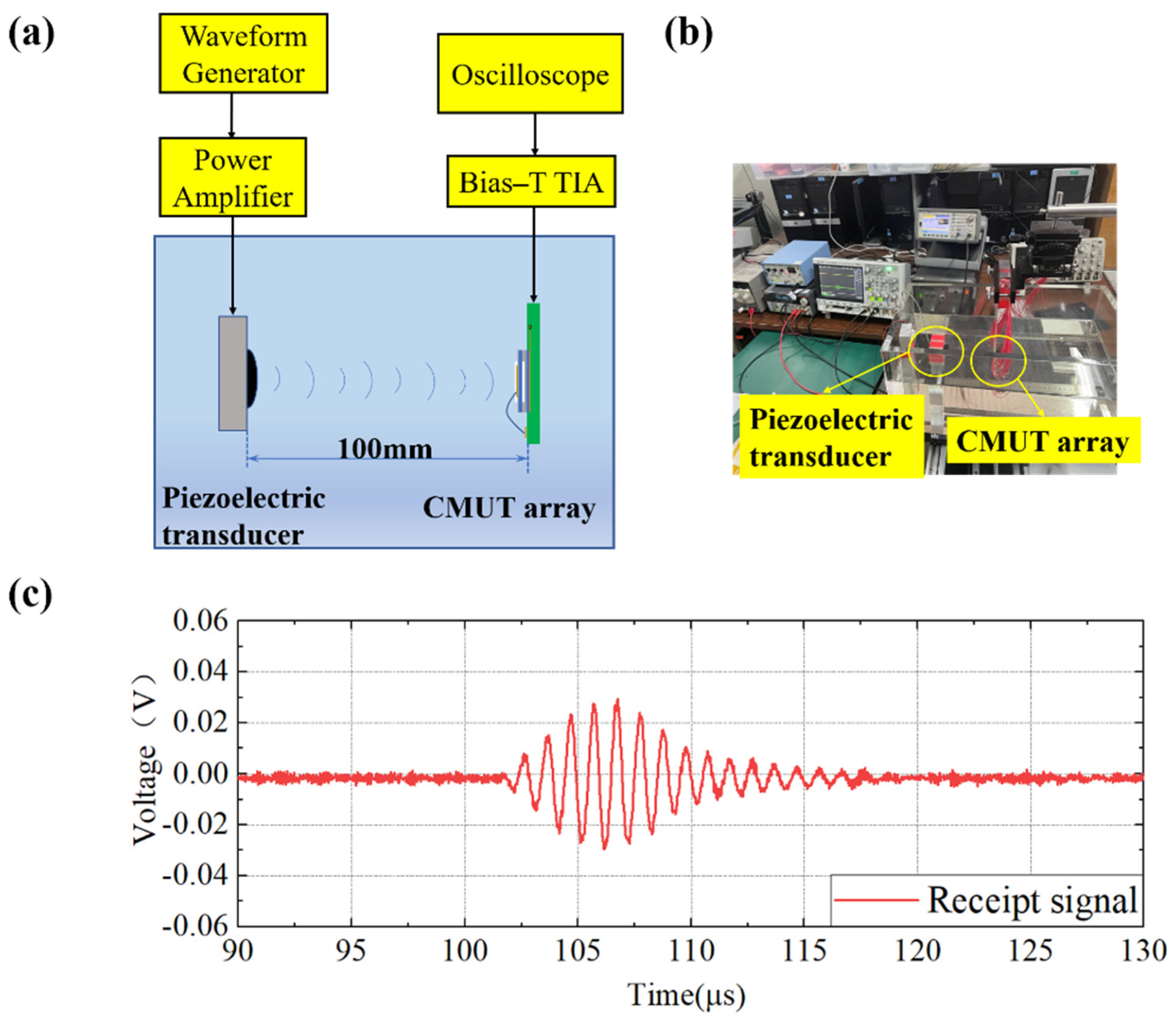
3.1. Acoustic Test
Acoustic Transceiver
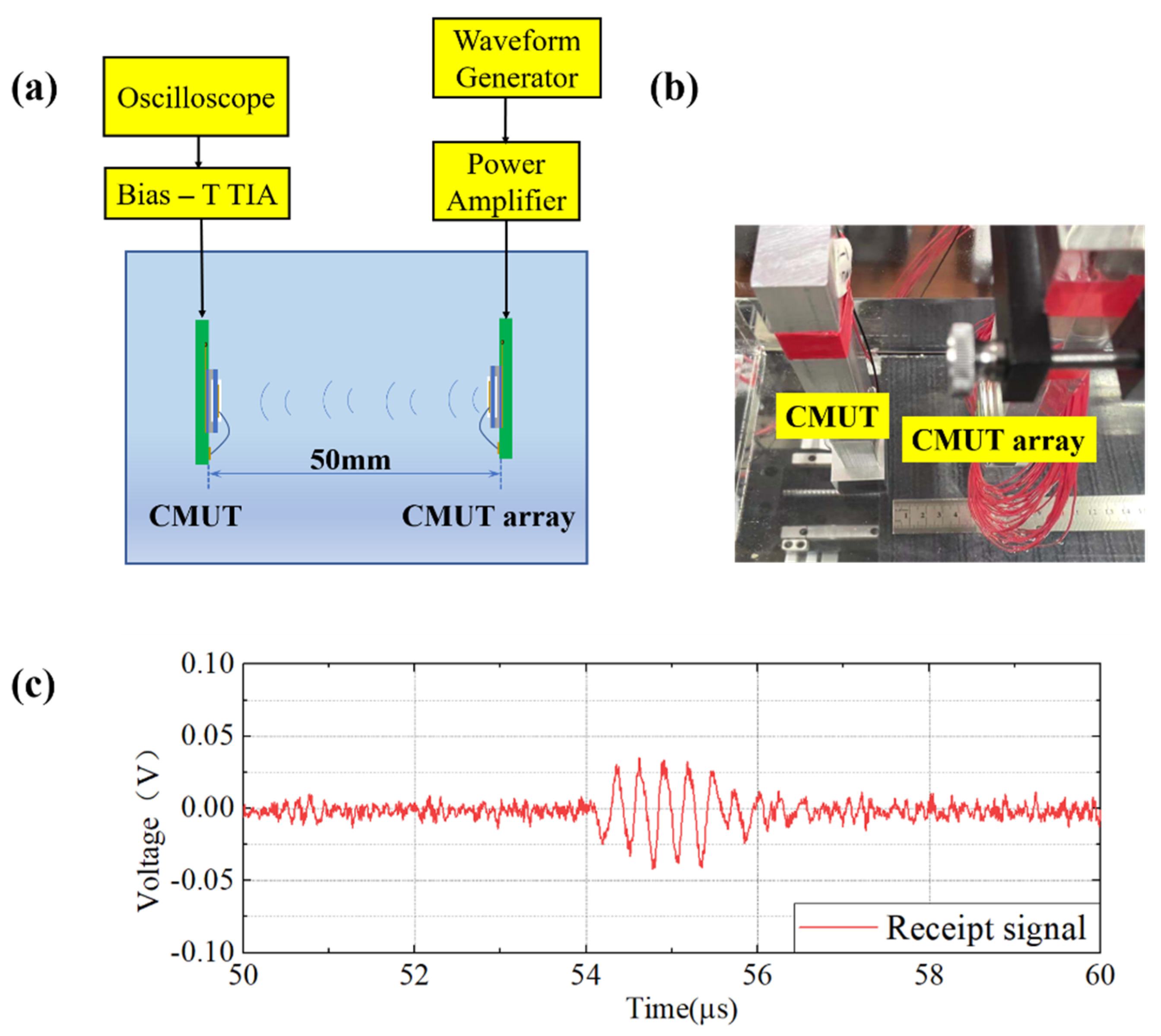
3.2. Transducer Performance Test
3.2.1. Bandwidth Test
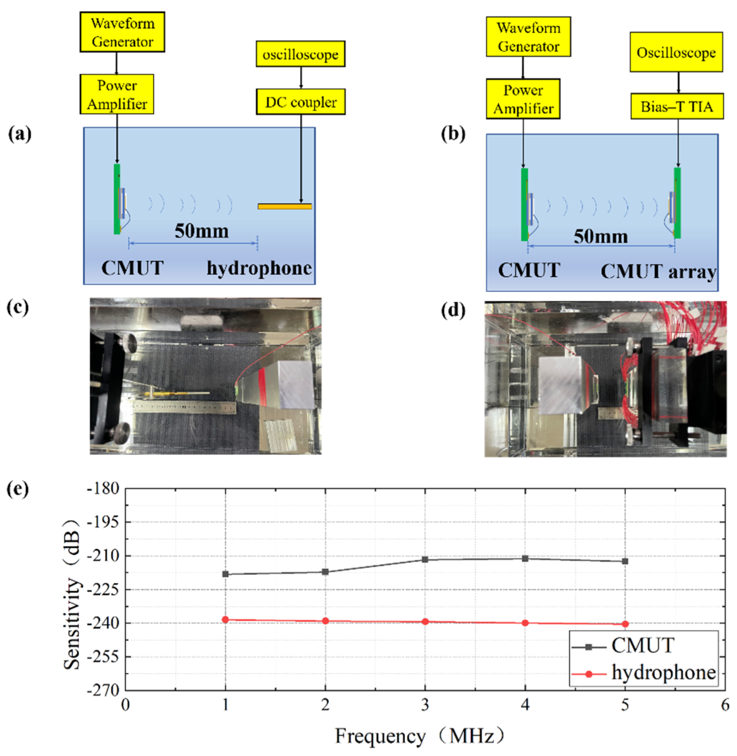
3.2.2. Receiving Sensitivity Test
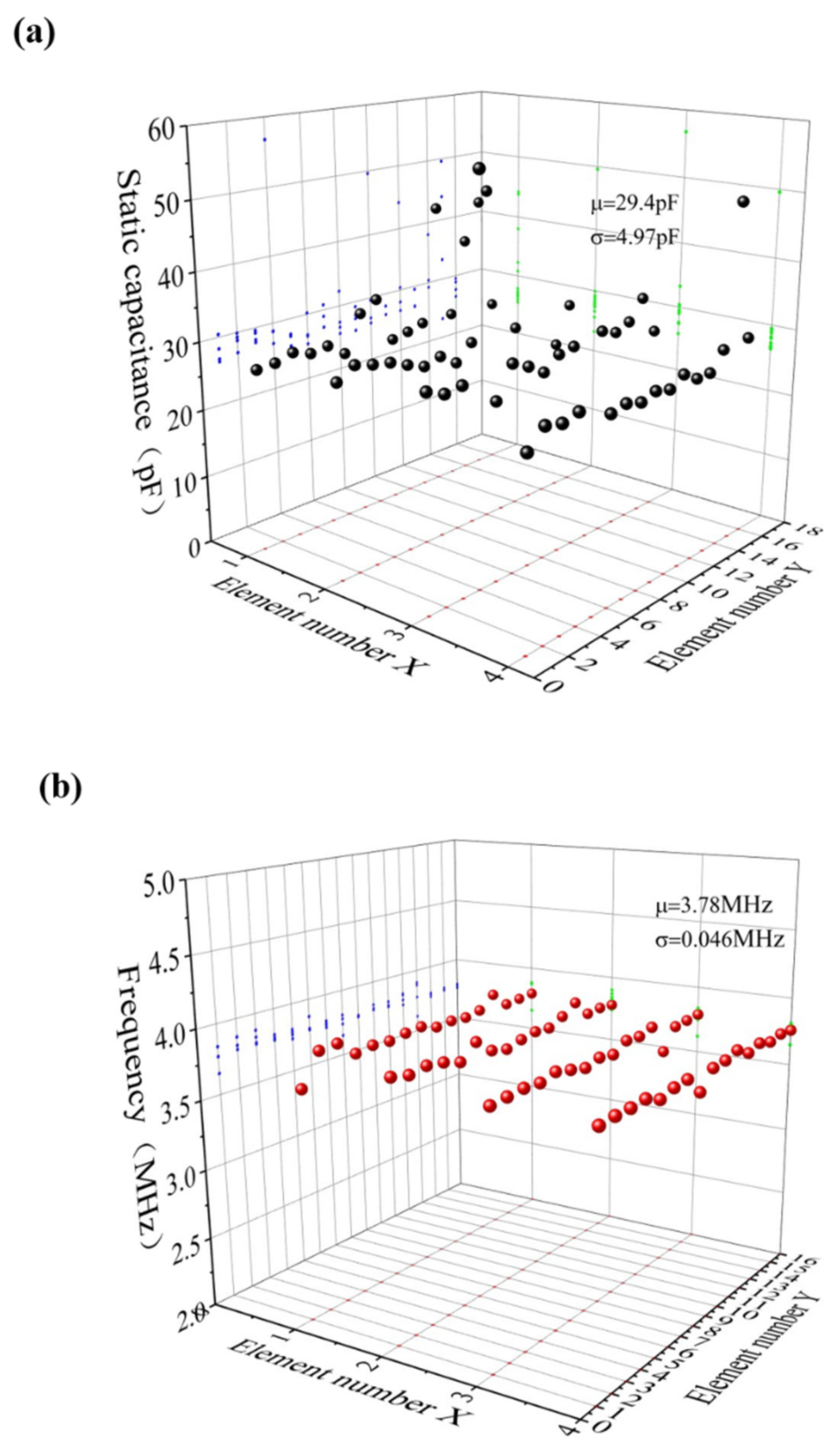
3.2.3. Conformance Testing
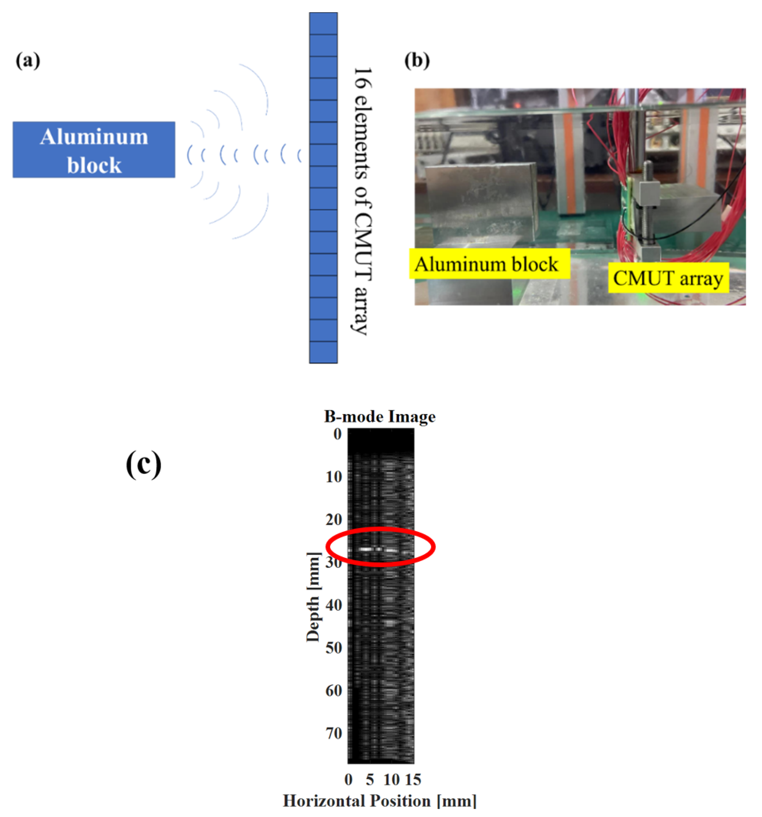
3.3. Underwater Imaging Experiment
4. Discussion
5. Conclusions
Author Contributions
Funding
Institutional Review Board Statement
Informed Consent Statement
Data Availability Statement
Conflicts of Interest
References
- Oralkan, O.; Ergun, A.S.; Johnson, J.A.; Karaman, M.; Demirci, U.; Kaviani, K.; Lee, T.H.; Khuri-Yakub, B.T. Capacitive Micromachined Ultrasonic Transducers: Next-Generation Arrays for Acoustic Imaging? IEEE Trans. Ultrason. Ferroelectr. Freq. Control 2002, 49, 1596–1610. [Google Scholar] [CrossRef] [PubMed]
- Erguri, A.S.; Huang, Y.; Zhuang, X.; Oralkan, O.; Yarahoglu, G.G.; Khuri-Yakub, B.T. Capacitive micromachined ultrasonic transducers: Fabrication technology. IEEE Trans. Ultrason. Ferroelectr. Freq. Control 2005, 52, 2242. [Google Scholar] [CrossRef]
- Fenster, A.; Tong, S.; Sherebrin, S.; Downey, D.B.; Rankin, R.N. Three-Dimensional Ultrasound Imaging. In Proceedings of the International Society for Optics and Photonics, Medical Imaging, San Diego, CA, USA, 8 May 1995; pp. 176–184. [Google Scholar]
- Jin, X.; Ladabaum, I.; Khuri-Yakub, B.T. The microfabrication of capacitive ultrasonic transducers. Microelectromech. Syst. J. 1998, 7, 295–302. [Google Scholar]
- Benacerraf, B.R.; Benson, C.B.; Abuhamad, A.Z.; Copel, J.A.; Abramowicz, J.S.; DeVore, G.R.; Doubilet, P.M.; Lee, W.; Lev-Toaff, A.S.; Merz, E.; et al. Three- and 4-Dimensional Ultrasound in Obstetrics and Gynecology. J. Ultrasound Med. 2005, 24, 1587–1597. [Google Scholar] [CrossRef]
- Hanprasertpong, T.; Hanaoka, U.; Zhang, X.; Mori, N.; Inubashiri, E.; Kanenishi, K.; Yamashiro, C.; Tanaka, H.; Shiota, A.; Yanagihara, T.; et al. Three-dimensional sonographic features of a fetus with Wolf-Hirschhorn syndrome. J. Med. Ultrason. 2008, 35, 197–199. [Google Scholar] [CrossRef] [PubMed]
- Hung, J.; Lang, R.; Flachskampf, F.; Shernan, S.K.; McCulloch, M.L.; Adams, D.B.; Thomas, J.; Vannan, M.; Ryan, T. 3D Echocardiography: A Review of the Current Status and Future Directions. J. Am. Soc. Echocardiogr. 2007, 20, 213–233. [Google Scholar] [CrossRef]
- Huang, Y.; Ergun, A.S.; Haeggstrom, E.; Badi, M.H.; Khuri-Yakub, B.T. Fabricating capacitive micromachined ultrasonic transducers with wafer-bonding technology. J. Microelectromech. Syst. 2003, 12, 128–137. [Google Scholar] [CrossRef] [Green Version]
- Caronti, A.; Savoia, A.; Caliano, G.; Pappalardo, M. Acoustic coupling in capacitive microfabricated ultrasonic transducers: Modeling and experiments. IEEE Trans Ultrason. Ferroelectr. Freq. Control 2005, 52, 2220–2234. [Google Scholar] [CrossRef] [PubMed]
- Alvarez-Arenas, T. Acoustic impedance matching of piezoelectric transducers to the air. IEEE Trans. Ultrason. Ferroelectr. Freq. Control 2004, 51, 624–633. [Google Scholar] [CrossRef]
- Lohfink, A.; Eccardt, P.C. Linear and nonlinear equivalent circuit modeling of CMUTs. IEEE Trans. Ultrason. Ferroelectr. Freq. Control 2006, 52, 2163–2172. [Google Scholar] [CrossRef]
- Schindel, D.W.; Hutchins, D.A.; Zou, L.; Sayer, M. The design and characterization of micromachined air-coupled capacitance transducers. IEEE Trans. Ultrason. Ferroelectr. Freq. Control 2002, 42, 42–50. [Google Scholar] [CrossRef]
- Gurun, G.; Tekes, C.; Zahorian, J.; Xu, T.; Satir, S.; Karaman, M.; Hasler, J.; Degertekin, F.L. Single-chip CMUT-on-CMOS front-end system for real-time volumetric IVUS and ICE imaging. IEEE Trans. Ultrason. Ferroelectr. Freq. Control 2014, 61, 239. [Google Scholar] [CrossRef] [PubMed] [Green Version]
- Attarzadeh, H.; Ytterdal, T. An in-probe low-noise low-power variable-gain receive amplifier for medical ultrasound imaging using CMUT transducers. Analog. Integr. Circuits Signal Processing 2017, 91, 73–81. [Google Scholar] [CrossRef]
- Um, J.; Kim, Y.; Cho, S.; Chae, M.; Song, J.; Kim, B.; Lee, S.; Bang, J.; Kim, Y.; Cho, K.; et al. An analog-digital hybrid RX beamformer chip with non-uniform sampling for ultrasound medical imaging with 2D CMUT array. IEEE Trans. Biomed. Circuits Syst. 2014, 8, 799–809. [Google Scholar] [CrossRef]
- Zhang, R.; Zhang, W.; He, C.; Song, J.; Mu, L.; Cui, J.; Zhang, Y.; Xue, C. Design of capacitive micromachined ultrasonic transducer (CMUT) linear array for underwater imaging. Sens. Rev. 2016, 36, 77–85. [Google Scholar] [CrossRef]
- Adelegan, O.J.; Coutant, Z.A.; Zhang, X.; Yamaner, F.Y.; Oralkan, Ö. Fabrication of 2D Capacitive Micromachined Ultrasonic Transducer (CMUT) Arrays on Insulating Substrates With Through-Wafer Interconnects Using Sacrificial Release Process. J. Microelectromech. Syst. 2020, 29, 553–561. [Google Scholar] [CrossRef]
- Park, K.K.; Lee, H.; Kupnik, M.; Khuri-Yakub, B.T. Fabrication of Capacitive Micromachined Ultrasonic Transducer Arrays With Isolation Trenches Using Anodic Wafer Bonding. IEEE Sens. J. 2015, 20, 95–103. [Google Scholar]
- Wygant, I.O.; Kupnik, M.; Windsor, J.C.; Wright, W.M.; Wochner, M.S.; Yaralioglu, G.G.; Hamilton, M.F.; Khuri-Yakub, B.T. 50 kHz Capacitive Micromachined Ultrasonic Transducers for Generation of Highly Directional Sound with Parametric Arrays. IEEE Trans. Ultrason. Ferroelectr. Freq. Control 2009, 56, 193–203. [Google Scholar] [CrossRef]
- Linder, S.; Baltes, H.; Gnaedinger, F.; Doering, E. Fabrication technology for wafer through-hole interconnections and three-dimensional stacks of chips and wafers. In Proceedings of the IEEE Micro Electro Mechanical Systems An Investigation of Micro Structures, Sensors, Actuators, Machines and Robotic Systems, Oiso, Japan, 25–28 January 1994. [Google Scholar]
- Song, J.; Xue, C.; He, C.; Zhang, R.; Mu, L.; Cui, J.; Miao, J.; Liu, Y.; Zhang, W. Capacitive Micromachined Ultrasonic Transducers (CMUTs) for Underwater Imaging Applications. Sensors 2015, 15, 23205–23217. [Google Scholar] [CrossRef] [PubMed] [Green Version]
- Attarzadeh, H.; Lim, S.K.; Ytterdal, T. Design and Analysis of a Stochastic Flash Analog-to-Digital Converter in 3D IC technology for integration with ultrasound transducer array. Microelectron. J. 2016, 48, 39–49. [Google Scholar] [CrossRef]
- Wygant, I.O.; Zhuang, X.; Yeh, D.T.; Oralkan, O.; Ergun, A.S.; Karaman, M.; Khuri-Yakub, B.T. Integration of 2D CMUT arrays with front-end electronics for volumetric ultrasound imaging. IEEE Trans. Ultrason. Ferroelectr. Freq. Control. 2008, 55, 327–342. [Google Scholar] [CrossRef] [PubMed]
- Khuriyakub, B.T.; Oralkan, Ö. Capacitive micromachined ultrasonic transducers for medical imaging and therapy. J. Micromech. Microeng. Struct. Devices Syst. 2011, 21, 54004. [Google Scholar] [CrossRef] [PubMed]
- Liu, T.; Ge, P.; Bi, W.; Wang, P. Fracture strength of silicon wafers sawn by fixed diamond wire saw. Sol. Energy 2017, 157, 427–433. [Google Scholar] [CrossRef]


| Parameter | Description/Dimension |
|---|---|
| Membrane shape | Round |
| Membrane diameter size | 100 µm |
| Membrane thickness | 2 µm |
| Cavity height | 0.3 µm |
| Electrode thickness | 0.5 µm |
| Trench width | 60 µm |
| Top electrode insulation layer thickness | 0.2 µm |
| Number of cells | 35 µm |
| Transducer dimensions | 1000 × 1000 µm |
Publisher’s Note: MDPI stays neutral with regard to jurisdictional claims in published maps and institutional affiliations. |
© 2022 by the authors. Licensee MDPI, Basel, Switzerland. This article is an open access article distributed under the terms and conditions of the Creative Commons Attribution (CC BY) license (https://creativecommons.org/licenses/by/4.0/).
Share and Cite
Wang, Z.; He, C.; Zhang, W.; Li, Y.; Gao, P.; Meng, Y.; Zhang, G.; Yang, Y.; Wang, R.; Cui, J.; et al. Fabrication of 2-D Capacitive Micromachined Ultrasonic Transducer (CMUT) Array through Silicon Wafer Bonding. Micromachines 2022, 13, 99. https://doi.org/10.3390/mi13010099
Wang Z, He C, Zhang W, Li Y, Gao P, Meng Y, Zhang G, Yang Y, Wang R, Cui J, et al. Fabrication of 2-D Capacitive Micromachined Ultrasonic Transducer (CMUT) Array through Silicon Wafer Bonding. Micromachines. 2022; 13(1):99. https://doi.org/10.3390/mi13010099
Chicago/Turabian StyleWang, Ziyuan, Changde He, Wendong Zhang, Yifan Li, Pengfei Gao, Yanan Meng, Guojun Zhang, Yuhua Yang, Renxin Wang, Jiangong Cui, and et al. 2022. "Fabrication of 2-D Capacitive Micromachined Ultrasonic Transducer (CMUT) Array through Silicon Wafer Bonding" Micromachines 13, no. 1: 99. https://doi.org/10.3390/mi13010099