
Macro-Modeling for N-Type Feedback Field-Effect Transistor for Circuit Simulation


ICT & Robotics Engineering and IITC, Hankyong National University, 327 Jungang-ro, Anseong-si 17579, Gyenggi-do, Korea
*
Author to whom correspondence should be addressed.
Micromachines 2021, 12(10), 1174; https://doi.org/10.3390/mi12101174
Submission received: 12 August 2021
/
Revised: 17 September 2021
/
Accepted: 26 September 2021
/
Published: 29 September 2021
(This article belongs to the Special Issue Nano Korea 2021)
Abstract
:In this study, we propose an improved macro-model of an N-type feedback field-effect transistor (NFBFET) and compare it with a previous macro-model for circuit simulation. The macro-model of the NFBFET is configured into two parts. One is a charge integrator circuit and the other is a current generator circuit. The charge integrator circuit consisted of one N-type metal-oxide-semiconductor field-effect transistor (NMOSFET), one capacitor, and one resistor. This circuit implements the charging characteristics of NFBFET, which occur in the channel region. For the previous model, the current generator circuit consisted of one ideal switch and one resistor. The previous current generator circuit could implement IDS-VGS characteristics but could not accurately implement IDS-VDS characteristics. To solve this problem, we connected a physics-based diode model with an ideal switch in series to the current generator circuit. The parameters of the NMOSFET and diode used in this proposed model were fitted from TCAD data of the NFBFET, divided into two parts. The proposed model implements not only the IDS-VGS characteristics but also the IDS-VDS characteristics. A hybrid inverter and an integrate and fire (I&F) circuit for a spiking neural network, which consisted of NMOSFETs and an NFBFET, were simulated using the circuit simulator to verify a validation of the proposed NFBFET macro-model.
1. Introduction
Recently, many problems occurring in designing next-generation integrated circuits (ICs) have been emerging, owing to continuous scaling for a metal-oxide-semiconductor field-effect transistor (MOSFET). The nanoscale MOSFET has a short channel effect, which increases the standby power by increasing leakage current, and has difficulty in controlling threshold voltage owing to the gate field influence becoming weak in a nanoscale channel [1,2]. Moreover, using MOSFETs to design high-performance ICs is difficult due to the physical limitations of MOSFETs being unable to have a subthreshold swing (SS) of less than 60 mV/dec at room temperature. To overcome these problems, various next-generation devices are suggested [3,4,5,6,7,8]. Among them, the family of Z2-FET (or field-effect diode) and feedback field-effect transistor (FBFET) with band-modulation operating mechanisms are in the spotlight for substituting the MOSFET [8,9,10,11,12]. The FBFET works on positive feedback in the channel region that is divided into two regions. One is a gated region and the other is an ungated region. These two regions form a potential barrier and potential well, respectively. The potential barrier and potential well, controlled by gate-source voltage and drain-source voltage, inject carriers into the potential well. Subsequently, positive feedback occurs in the channel region. The energy band of the channel region changes abruptly from S-shape to parallel, owing to the positive feedback. These characteristics of the FBFET cause a high on/off current ratio and a sharp increase and decrease in the forward sweep and the reverse sweep, respectively. Furthermore, the FBFET has hysteresis characteristics that are caused by a difference in the threshold voltage of the forward and reverse sweeps. Various applications of the FBFET utilizing these characteristics have been studied. The electrical characteristics of the FBFET have been investigated using the FBFET as a logic gate [10,11,12,13,14,15,16]. In addition, memory circuits, neuromorphic circuits, and biosensors consisting of FBFETs or hybrid components (e.g., the FBFET and the MOSFET) were investigated utilizing charging in the channel region and the hysteresis characteristics [17,18,19,20,21,22].
The various applications of the FBFET can be analyzed using technology computer-aided design (TCAD) [23]. TCAD mixed-mode [23] is a powerful tool for investigating the electrical characteristics of the various types of circuit consisting of FBFETs. However, to analyze and simulate the very large-scaled ICs consisting of FBFETs or hybrid components, a compact model of FBFET for circuit simulation is needed. Thus far, compact models of FBFET have been studied with physics-based analytical equations [24,25,26], and yet, only one macro-model based on an equivalent circuit consisting of only Simulation Program with Integrated Circuit Emphasis (SPICE) devices has been reported. The reported macro-model of FBFET consists of two circuits [27]. One is a charge integration circuit and the other is a current generation circuit. The charge integration circuit is composed of one MOSFET and one capacitor, and the current generation circuit consists of one ideal switch and one resistor. This model has a limitation on implementing the IDS-VDS characteristics of FBFET. Therefore, there is a problem in simulating the memory circuits or neuromorphic circuits with SPICE using that model. To simulate the circuits consisting of the FBFETs or hybrid components, solutions to overcome these limitations are required.
In this paper, we propose an improved FBFET macro-model that can implement not only IDS-VGS characteristics but also IDS-VDS characteristics by adding one physics-based diode model to the model presented previously by another group. First, the electrical characteristics and the macro-model configuration of the FBFET are discussed in Section 2. Thereafter, the parameter extraction of the MOSFET and diode used in this proposed model is described, and SPICE simulation results of the proposed macro-model are discussed in Section 3. Finally, the conclusions of this study are discussed in Section 4.
2. Macro-Modeling of FBFET
2.1. FBFET Mechanism
Figure 1a shows a 2D schematic diagram of an N-type FBFET (NFBFET). Figure 1b shows the energy band diagrams of the NFBFET at off states (VGS = VDS = 0 V). Figure 1c,d shows the energy band diagrams at VDS = 1 V and different VGS, and at VGS = 0.6 V and different VDS, respectively. In Figure 1c,d, the red and black lines denote on and off states of the NFBFET, respectively, and the symbols e- and h+ represent electron and hole, respectively. Moreover, the black dotted lines denote energy band of near-threshold voltage of the forward sweep. The FBFET structure is a p-i-n diode structure (Z2-FET) [28] with a high-doped n-p diode in the channel region. As the drain-source voltage (VDS) or the gate-source voltage (VGS) are not applied, the drain-source region forms potential barriers, as shown in Figure 1b. Therefore, the carriers are not injected into the channel region. To make the electrons (holes) flow from (to) the source to (from) the drain, appropriate VDS and VGS must be applied to eliminate potential barriers. The energy band diagrams, as shown in Figure 1c,d, represent the carriers’ flow over the threshold of VGS and VDS = 1 V, as well as over the threshold of VDS and VGS = 0.6 V, respectively. In Figure 1c, when VGS is applied at VDS = 1 V, the potential barrier (gated channel region) is lower. The electron from the source region is injected into the potential well (ungated channel region). Thereafter, the accumulated electrons make the potential well higher. The hole, which cannot flow into the channel region by the potential well, can be injected into the channel region. This positive feedback rapidly eliminates the potential barrier and potential well. In the end of the forward sweep, the energy band of the NFBFET is aligned, as denoted by the red line in Figure 1c. In Figure 1d, when VDS is applied at VGS = 0.6 V, the electrons from the source region are injected into the channel region (ungated channel region). The positive feedback occurs with the same mechanism mentioned in Figure 1c. By these characteristics, the NFBFET has a high on/off ratio. Moreover, the NFBFET has hysteresis characteristics, owing to differences between the forward and reverse sweeps.
2.2. TCAD Simulation
Table 1 shows the structure parameters of the NFBFET. The total length of the NFBFET is 140 nm. The oxide material used in the simulation is aluminum oxide (Al2O3). To simulate the NFBFET, the MOSFET and bipolar junction transistor models were used. Those models include the Lombardi concentration, voltage, and temperature model (CVT), Shockley–Read–Hall model (SRH), Fermi–Dirac calculation, field-dependent mobility model (FLDMOB), Auger recombination model (AUGER), and band gap narrowing model (BGN). The simulation temperature was 300 K, and the TCAD simulator Atlas by Silvaco was used for simulation [23]. Figure 2a,b shows the TCAD simulation results of the drain-source currents to gate-source voltage (IDS-VGS) characteristics at VDS = 1 V and drain-source currents to drain-source voltage (IDS-VDS) characteristics at VGS = 0.6 V of NFBFET. Voltage directions of the forward and reverse sweeps are indicated by the dashed arrows in Figure 2. The NFBFET has a memory window that is the difference in threshold voltage between forward and reverse sweeps. The memory windows of the NFBFET are 0.53 V and 2.06 V for the IDS-VGS characteristics and IDS-VDS characteristics, respectively.
2.3. Macro-Model of NFBFET
Figure 3a,b shows the equivalent circuits of the previous macro-model [27] and the proposed macro-model of NFBFET, respectively. Both NFBFET macro-models consist of two parts. One is a charge integration circuit consisting of one voltage source, one N-type MOSFET (NMOSFET), one capacitor, and one resistor. The other is a current generation circuit consisting of one resistor and one ideal switch. The charge integration circuit implements the charging characteristics of charges in the channel region of the FBFET. The charges accumulated on the potential well in the channel region are integrated into the capacitor Cbody. The current generation circuit implements generating the on/off current by switching the ideal switch. In the previous model (Figure 3a), the current generation circuit works by using only an ideal switch with a simple diode equation. Since the simple diode equation in the previous model is used, it is difficult to exactly fit IDS-VDS characteristics and the on-current of FBFET by using only one parameter Ioff. This is valid only for the IDS-VGS characteristics. However, for the IDS-VDS characteristics, the NFBFET has diode characteristics in reverse sweep, as shown in Figure 2b. To implement the IDS-VDS characteristics more precisely, the physics-based diode model (red dotted circle) embedded in SPICE, as shown in Figure 3b, is connected at the ideal switch in series for the proposed model. For the SPICE simulation using the proposed macro-model of NFBFET, the Berkeley Short-channel IGFET Model - Independent Multi-Gate (BSIM-IMG, level = 301, version 102.7.0) [29,30] model was used for the MOSFET, the diode (level = 3) model was used for diode model, and the SmartSpice program was used for the simulation [31].
3. SPICE Simulation Results
3.1. Parameter Fitting
The NFBFET was divided into two parts for the parameter fitting. One is a p-n junction from the drain region for the diode, and the other is an n-p-n structure from the source region for the NMOSFET, as shown in Figure 1a. This concept came from a geometric view of the NFBFET. The parameters of the BSIM-IMG model for the NMOSFET and the diode (level = 3) model were first fitted with the TCAD data of the NFBFET. The parameters of the BSIM-IMG model and diode model were extracted, as shown in Table 2. In the equivalent circuit, the values of other components are Cbody = 1 pF, Rbody = 450 Ω, VT = 0.000610945 V, VH = 0.000290705 V, Roff = 1/Ioff = 1/(6.496 × 10−15) Ω, and Ron = 1 Ω.
Figure 4a shows the results of the diode parameter fitting. The square symbols and black lines denote the simulation results by TCAD and SPICE, respectively. There were mismatches at a high field (>1.3 V) for linear plot and at a low field (~0.4 V) for log plot. These were caused by difficulties in fitting the parameter of a heavily doped diode. Figure 4b,c shows IDS-VGS characteristics and IDS-VDS characteristics of NMOSFET in NFBFET, respectively. The square symbols and solid lines denote the simulation results by TCAD and SPICE, respectively. Likewise, there were mismatches for both results. These mismatches were caused by fitting the heavily doped channel of MOSFET, since the BSIM-IMG model was limited to below 5 × 1018 cm−3 in terms of the channel doping concentration [29,30].
3.2. SPICE Results of Macro-Model
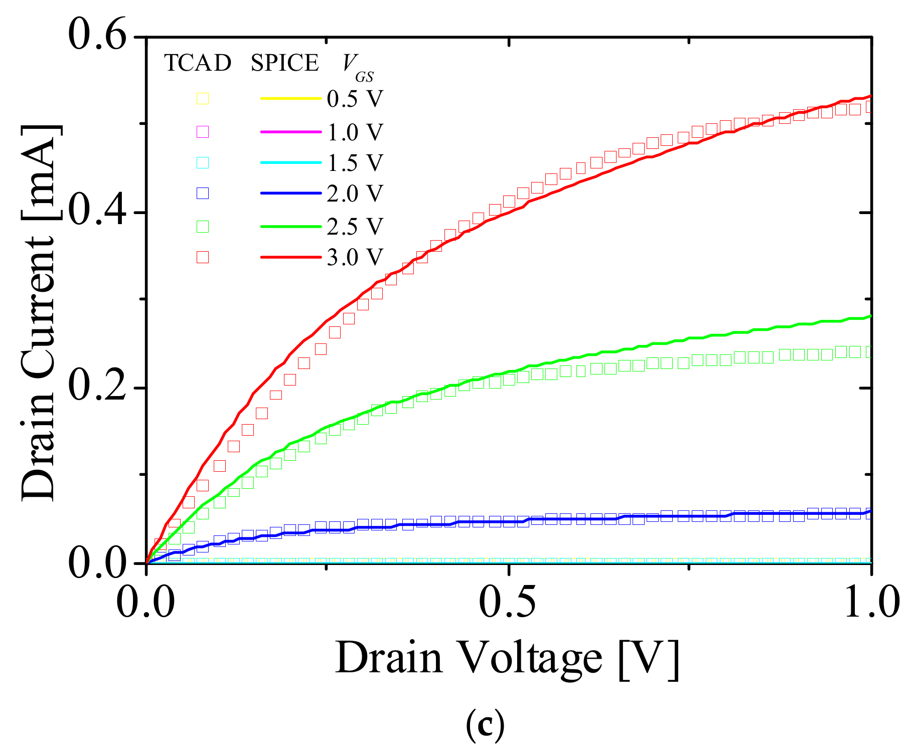
Figure 5a,b shows IDS-VGS characteristics and IDS-VDS characteristics of the NFBFET, respectively. The symbols and lines denote the simulation results by TCAD and macro-model of SPICE, respectively. For the IDS-VGS characteristics, both results at VGS = 1 V and VGS = 0.8 V were fitted with TCAD data in terms of threshold voltages. However, for the subthreshold region and VDS below 0.8 V, there were mismatches. In particular, for the reverse sweep, the threshold voltage mismatches were observed at VDS below 0.8 V. The IDS-VGS characteristics are implemented by an ideal switch in the current generation circuit. The ideal switch only made an on/off current; therefore, these characteristics caused mismatches near the threshold voltage and at the subthreshold region, as shown in Figure 5a. For the IDS-VDS characteristics, the hysteresis characteristics occur under specific conditions, which are controlled by sustaining drain voltage with continuity of diffusion and generation-recombination currents in the channel region [28]. The hysteresis characteristics only occur near VGS = 0.6 V, as shown in Figure 5b. Likewise, there were mismatches in the subthreshold region and on-current as the BSIM-IMG and diode model used for the macro-model have a limitation in terms of heavily doped channel, as described in Section 3.1.
3.3. Model Validation
Figure 6 shows IDS-VDS characteristics of NFBFET. The squares and solid lines denote the experimental data and fitted SPICE results, respectively. The experimental results are from the Z2-FET structure with 28 nm fully depleted silicon-on insulator (FDSOI) fabrication [16]. Although this NFBFET structure is not the same as the one in Figure 1a, the proposed macro-model of NFBFET can fit the electrical characteristics for the same operating mechanism, as shown in Figure 6. The parameters of the proposed macro-model of NFBFET were changed to VT = 0.00032591 V and VH = 0.00032591 V for the ideal switch model and RS = 1 × 10⁻⁶ Ω·m2 for the diode model. The small mismatches in the parameter fitting result occurred due to the limitation of the models, as described in Section 3.1.
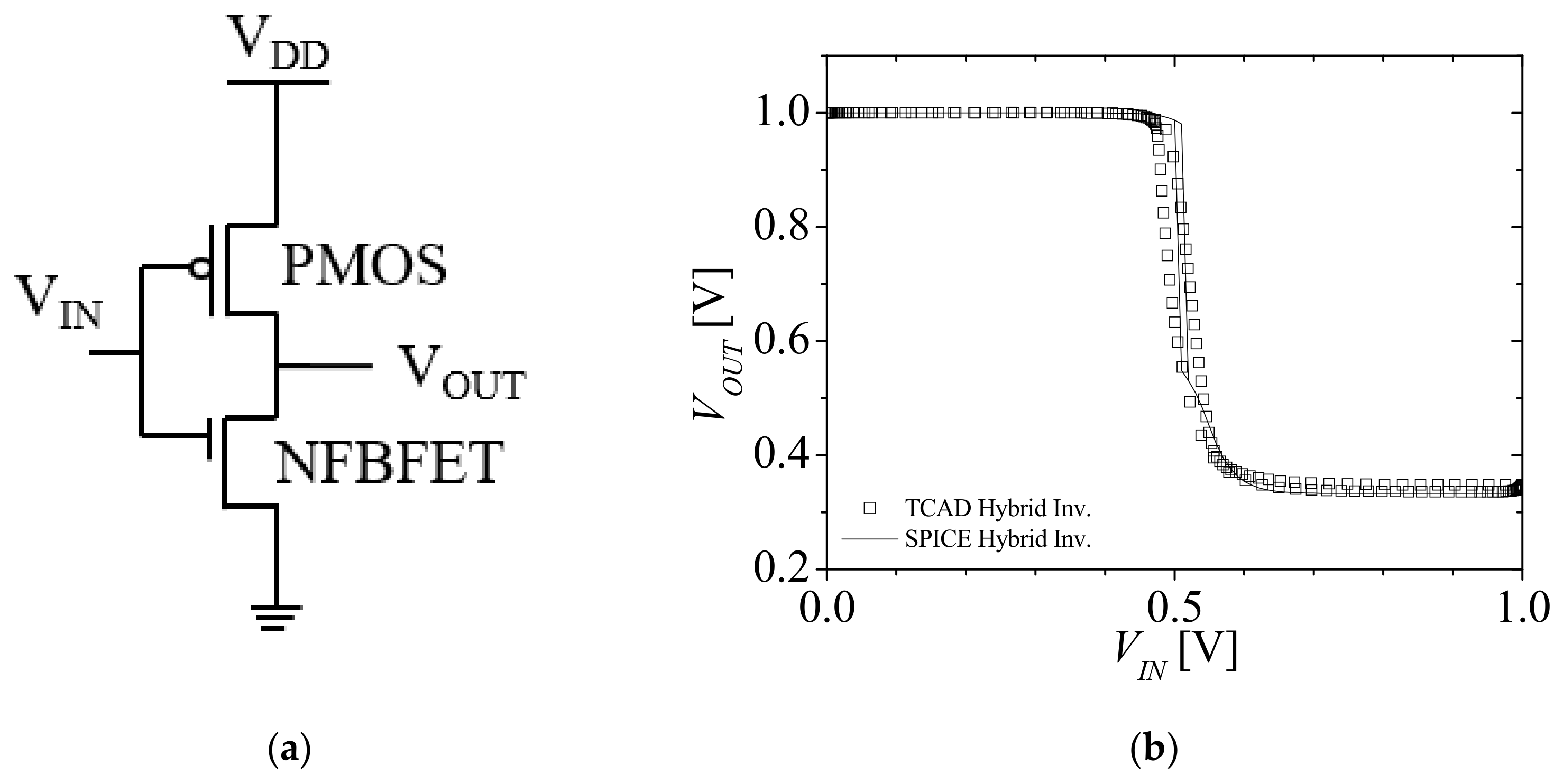
Figure 7a,b shows a circuit diagram of a hybrid inverter, which consists of P-type MOSFET (PMOSFET) and NFBFET, as shown in Figure 1a, and the voltage transfer characteristics (VTC) of the hybrid inverter, respectively. The square symbols and solid lines denote VTCs simulated with TCAD and macro-model of SPICE, respectively, as shown in Figure 7b. The VTC by TCAD has a switching voltage gap caused by the threshold voltage difference between forward and reverse sweeps. The VTC for the macro-model also has a switching voltage gap, but the switching slope is extremely sharp compared with the TCAD results. These characteristics were caused by the hysteresis voltage control of the ideal switch model composed in the current generation circuit.
Figure 8a shows the circuit diagram of an integrate and fire (I&F) circuit for a spiking neural network (SNN) [21]. Complementary MOS (CMOS)-based I&F circuits have a number of MOSFETs for implementing spike and reset mechanisms; therefore the circuits have a high power consumption. To overcome this problem, the other research team suggested an I&F circuit that consisted of the NFBFET. The NFBFET has the capability to accumulate charge in the channel region. Using these characteristics, the spike and reset mechanism can be implemented. Moreover, the NFBFET replaces a number of transistors, which significantly reduces system area and power consumption. Figure 8b show the results of SPICE simulation for an I&F circuit consisting of a macro-model of NFBFET, as shown in Figure 1a. The black line, red line, and square symbols denote synaptic current (Isynaptic), membrane voltage (VMB), and spike voltage (Vspike), respectively. Word line 1 (VWL1) and word line 2 (VWL2) voltages were applied at 0.6 V and 0.1 V, respectively. The spike operation occurred for the I&F consisting of a macro-model, but the complete reset operation was not performed, as shown in Figure 8b. This was due to the magnitude of hysteresis characteristics of the macro-model.
4. Conclusions
In this paper, we proposed an improved macro-model of an NFBFET compared with a previous model. The previous model was configured with a charge integration circuit and a current generation circuit. The current generation circuit of the previous model has a limitation that cannot implement IDS-VDS characteristics. To solve this problem, we added a diode into the current generation circuit. First, for simulating the NFBFET with the proposed macro-model using SPICE, the parameters of the NMOSFET and diode composed in the model were fitted with the simulation results of the NFBFET and diode by TCAD. The fitted results of the diode and NMOSFET had mismatches in the subthreshold region and high field region. These mismatches were caused by a p-n-p-n structure with only a heavily doped region (1020 cm−3). The parameters of the NMOSFET and diode in the macro-model of NFBFET were extracted from the simulation results by TCAD. The SPICE simulation results of the macro-model of NFBFET had mismatches near the threshold voltage and at the subthreshold region. These mismatches were caused by a limitation that implemented transfer characteristics using the diode and ideal switch. Finally, for validating the macro-model of the NFBFET, a parameter fitting was conducted with experimental data, and a hybrid inverter and an I&F circuit, which included a MOSFET and a NFBFET, were simulated by SPICE. The fitted results using the parameters extracted from the experimental data show that the macro-model of the NFBFET can implement the electrical characteristics for the same operating mechanism. The VTC of TCAD and macro-model had a switching voltage gap, but the switching slope of the macro-model was extremely sharp, owing to an ideal switch in the current generation circuit. The I&F circuit generated spike operation, but the complete reset operation was not performed due to the limitation of hysteresis characteristics. To overcome the limitations such as the mismatch around the threshold voltages of the macro-model of NFBFET consisting of MOSFET and the other devices, improvements in the proposed macro-model or the analytical modeling of FBFET are required. Moreover, since the proposed structure may include leakage currents such as band-to-band tunneling (BTBT), an improved macro-model development and parameter extractions are required.
Author Contributions
Conceptualization, J.H.O. and Y.S.Y.; methodology, J.H.O. and Y.S.Y.; investigation, J.H.O. and Y.S.Y.; data curation, J.H.O.; writing—original draft preparation, J.H.O.; writing—review and editing, J.H.O. and Y.S.Y.; supervision, Y.S.Y.; project administration, Y.S.Y.; funding acquisition, Y.S.Y. Both authors have read and agreed to the published version of the manuscript.
Funding
This research was supported by the Basic Science Research Program through NRF of Korea funded by the Ministry of Education (NRF-2019R1A2C1085295).
Acknowledgments
This work was supported by IDEC (EDA tool).
Conflicts of Interest
The authors declare no conflict of interest.
References
- Zhao, W.; Cao, Y. New Generation of Predictive Technology Model for Sub-45 nm Early Design Exploration. IEEE Trans. Electron Devices 2006, 53, 2816–2823. [Google Scholar] [CrossRef]
- Khakifirooz, A.; Antoniadis, D.A. MOSFET Performance Scaling-Part I: Historical Trends. IEEE Trans. Electron Devices 2008, 55, 1391–1400. [Google Scholar] [CrossRef]
- Cristoloveanu, S.; Wan, J.; Zaslavsky, A. A Review of Sharp-Switching Devices for Ultra-Low Power Applications. IEEE J. Electron Devices Soc. 2016, 4, 215–226. [Google Scholar] [CrossRef]
- Choi, W.Y.; Park, B.-G.; Lee, J.D.; Liu, T.-J.K. Tunneling Field-Effect Transistors (TFETs) With Subthreshold Swing (SS) Less Than 60 mV/dec. IEEE Electron Device Lett. 2007, 28, 743–745. [Google Scholar] [CrossRef]
- Kam, H.; Lee, D.T.; Howe, R.T.; King, T.-J. A new nano-electro-mechanical field effect transistor (NEMFET) design for low-power electronics. In Proceedings of the IEEE International Electron Devices Meeting (IEDM), Washington, DC, USA, 5 December 2005; pp. 463–466. [Google Scholar] [CrossRef]
- Khan, A.I.; Yeung, C.W.; Hu, C.; Salahuddin, S. Ferroelectric negative capacitance MOSFET: Capacitance tuning & antiferroelectric operation. In Proceedings of the 2011 International Electron Devices Meeting (IEDM), Washington, DC, USA, 5–7 December 2011; pp. 11.3.1–11.3.4. [Google Scholar] [CrossRef]
- Gopalakrishnan, K.; Griffin, P.B.; Plummer, J.D. I-MOS: A novel semiconductor device with a subthreshold slope lower than kT/q. In Proceedings of the Digest, International Electron Devices Meeting (IEDM), San Francisco, CA, USA, 8–11 December 2002; pp. 289–292. [Google Scholar] [CrossRef]
- Solaro, Y.; Wan, J.; Fonteneau, P.; Fenouillet-Beranger, C.; Le Royer, C.; Zaslavsky, A.; Ferrari, P.; Cristoloveanu, S. Z2-FET: A promising FDSOI device for ESD protection. Solid State Electron. 2014, 97, 23–29. [Google Scholar] [CrossRef]
- Dirani, H.E.; Solaro, Y.; Fonteneau, P.; Ferrari, P.; Cristoloveanu, S. Properties and mechanism of Z2-FET at variable temperature. Solid State Electron. 2016, 115, 201–206. [Google Scholar] [CrossRef]
- Wan, J.; Le Royer, C.; Zaslavsky, A.; Cristoloveanu, S. Z2-FET: A zero-slope switching device with gate-controlled hysteresis. In Proceedings of the Technical Program of 2012 VLSI Technology, System and Application, Hsinchu, Taiwan, 23–25 April 2012; pp. 1–4. [Google Scholar] [CrossRef]
- Lee, C.; Ko, E.; Shin, C. Steep slope silicon-on-insulator feedback field-effect transistor: Design and performance analysis. IEEE Trans. Electron Devices 2019, 66, 286–291. [Google Scholar] [CrossRef]
- Lee, C.; Sung, J.; Shin, C. Understanding of Feedback Field-Effect Transistor and Its Applications. Appl. Sci. 2020, 10, 3070. [Google Scholar] [CrossRef]
- Oh, J.H.; Yu, Y.S. Investigation of monolithic 3D integrated circuit inverter with feedback field effect transistors using TCAD simulation. Micromachines 2020, 11, 852. [Google Scholar] [CrossRef] [PubMed]
- Kwon, M.-W.; Hwang, S.; Baek, M.-H.; Cho, S.; Park, B.-G. Dual gate positive feedback field-effect transistor for low power analog circuit. In Proceedings of the 2017 Silicon Nanoelectronics Workshop (SNW), Kyoto, Japan, 4–5 June 2017; pp. 115–116. [Google Scholar] [CrossRef]
- Wan, J.; Royer, C.L.; Zaslavsky, A.; Cristoloveanu, S. A systematic study of the sharp-switching Z2-FET device: From mechanism to modeling and compact memory applications. Solid State Electron. 2013, 90, 2–11. [Google Scholar] [CrossRef]
- Lee, K.H.; El Dirani, H.; Fonteneau, P.; Bawedin, M.; Cristoloveanu, S. Sharp Logic Switch Based on Band Modulation. IEEE Electron Device Lett. 2019, 40, 1852–1855. [Google Scholar] [CrossRef]
- Yeung, C.W.; Padilla, A.; Liu, T.-J.K.; Hu, C. Programming characteristics of the steep turn-on/off feedback FET (FBFET). In Proceedings of the 2009 Symposium on VLSI Technology, Kyoto, Japan, 15–17 June 2009; pp. 176–177. [Google Scholar]
- Kang, H.; Cho, J.; Kim, Y.; Lim, D.; Woo, S.; Cho, K.; Kim, S. Nonvolatile and volatile memory characteristics of a silicon nanowire feedback field-effect transistor with a nitride charge-storage layer. IEEE Trans. Electron Devices 2019, 66, 3342–3348. [Google Scholar] [CrossRef]
- Cho, J.; Lim, D.; Woo, S.; Cho, K.; Kim, S. Static Random Access Memory Characteristics of Single-Gated Feedback Field-Effect Transistors. IEEE Trans. Electron Devices 2019, 66, 413–419. [Google Scholar] [CrossRef]
- Kwon, M.-W.; Park, K.; Baek, M.-H.; Lee, J.; Park, B.-G. A Low-Energy High-Density Capacitor-Less I&F Neuron Circuit Using Feedback FET Co-Integrated With CMOS. IEEE J. Electron Devices Soc. 2019, 7, 1080–1084. [Google Scholar] [CrossRef]
- Woo, S.; Cho, J.; Lim, D.; Park, Y.-S.; Cho, K.; Kim, S. Implementation and Characterization of an Integrate-and-Fire Neuron Circuit Using a Silicon Nanowire Feedback Field-Effect Transistor. IEEE Trans. Electron Devices 2020, 67, 2995–3000. [Google Scholar] [CrossRef]
- Singh, D.; Patil, G.C. Performance Analysis of Feedback Field-Effect Transistor Based Biosensor. IEEE Sens. J. 2020, 20, 13269–13276. [Google Scholar] [CrossRef]
- Silvaco Int. ATLAS ver. 5. 30. 0. R Manual; Silvaco Int.: Santa Clara, CA, USA, 2015. [Google Scholar]
- Martinie, S.; Lacord, J.; Lee, K.; Bawedin, M.; Cristoloveanu, S. Pragmatic Z2-FET compact model including DC and 1T-DRAM memory operation. Solid State Electron. 2021, 179, 107960. [Google Scholar] [CrossRef]
- Martinie, S.; Lacord, J.; Rozeau, O.; Parihar, M.-S.; Lee, K.; Bawedin, M.; Cristoloveanu, S.; Taur, Y.; Barbe, J.-C. Z2-FET SPICE model: DC and memory operation. In Proceedings of the 2017 IEEE SOI-3D-Subthreshold Microelectronics Technology Unified Conference (S3S), Burlingame, CA, USA, 16–19 October 2017. [Google Scholar] [CrossRef]
- Lacord, J.; Martinie, S.; Parihar, M.-S.; Lee, K.; Bawedin, M.; Cristoloveanu, S.; Taur, Y.; Barbé, J.-C. Z2-FET DC hysteresis: Deep understanding and preliminary model. In Proceedings of the 2017 International Conference on Simulation of Semiconductor Processes and Devices (SISPAD), Kamakura, Japan, 7–9 September 2017; pp. 321–324. [Google Scholar]
- Kwon, M.-W.; Park, K.; Baek, M.-H.; Hwang, S.; Jang, T.; Park, B.-G. Simulation Program with Integrated Circuit Emphasis Compact Modeling of a Dual-Gate Positive-Feedback Field-Effect Transistor for Circuit Simulations. J. Nanosci. Nanotechnol. 2019, 19, 6417–6421. [Google Scholar] [CrossRef] [PubMed]
- Taur, Y.; Lacord, J.; Singh Parihar, M.; Wan, J.; Martinie, S.; Lee, K.-H.; Bawedin, M.; Barbe, J.-C.; Cristoloveanu, S. A comprehensive model on field-effect pnpn devices (Z2-FET). Solid State Electron. 2017, 134, 1–8. [Google Scholar] [CrossRef]
- Hu, C.; Niknejad, A.; Sriramkumar, V.; Lu, D.; Chauhan, Y.; Kahm, M.; Sachid, A. BSIM-IMG: A Turnkey compact model for fully depleted technologies. In Proceedings of the 2012 IEEE International SOI Conference (SOI), Napa, CA, USA, 1–4 October 2012; pp. 1–24. [Google Scholar] [CrossRef]
- Silvaco Int. SPICE Models Manual; Silvaco Int.: Santa Clara, CA, USA, 2015. [Google Scholar]
- Silvaco Int. SmartSpice ver. 4. 44. 3. R Manual; Silvaco Int.: Santa Clara, CA, USA, 2015. [Google Scholar]
Figure 1.
(a) Schematic diagram of an N–type feedback field–effect transistor (NFBFET). The energy band diagrams of the NFBFET; (b) at off state (VDS = 0 V and VGS = 0 V); (c) at VDS = 1 V and different VGS; and (d) at VGS = 0.6 V and different VDS.
Figure 1.
(a) Schematic diagram of an N–type feedback field–effect transistor (NFBFET). The energy band diagrams of the NFBFET; (b) at off state (VDS = 0 V and VGS = 0 V); (c) at VDS = 1 V and different VGS; and (d) at VGS = 0.6 V and different VDS.

Figure 2.
(a) IDS-VGS characteristics at VDS = 1 V; (b) IDS-VDS characteristics at VGS = 0.6 V.

Figure 3.
Circuit diagram of (a) the previous macro-model and (b) the proposed macro-model.


Figure 4.
Diode parameter fitting data (a) and metal–oxide–semiconductor field–effect transistor (MOSFET) parameter fitting data for (b) IDS-VGS characteristics, and (c) IDS-VDS characteristics.
Figure 4.
Diode parameter fitting data (a) and metal–oxide–semiconductor field–effect transistor (MOSFET) parameter fitting data for (b) IDS-VGS characteristics, and (c) IDS-VDS characteristics.


Figure 5.
Simulation Program with Integrated Circuit Emphasis (SPICE) results of macro–model of NFBFET for (a) IDS-VGS characteristics and (b) IDS-VDS characteristics.
Figure 5.
Simulation Program with Integrated Circuit Emphasis (SPICE) results of macro–model of NFBFET for (a) IDS-VGS characteristics and (b) IDS-VDS characteristics.


Figure 6.
IDS–VDS characteristics: Symbols and lines denote experimental data and simulation results with the parameter extracted from experimental data [16], respectively.
Figure 6.
IDS–VDS characteristics: Symbols and lines denote experimental data and simulation results with the parameter extracted from experimental data [16], respectively.

Figure 7.
Circuit diagram of (a) a hybrid inverter and (b) the voltage transfer characteristics (VTCs) for TCAD and SPICE.
Figure 7.
Circuit diagram of (a) a hybrid inverter and (b) the voltage transfer characteristics (VTCs) for TCAD and SPICE.

Figure 8.
Circuit diagram of (a) an integrate and fire circuit for spiking neural network (SNN) and (b) synaptic current, membrane voltage, and spike voltage.
Figure 8.
Circuit diagram of (a) an integrate and fire circuit for spiking neural network (SNN) and (b) synaptic current, membrane voltage, and spike voltage.


Table 1.
Structure parameters of the NFBFET used in technology computer-aided design (TCAD) simulation.
Table 1.
Structure parameters of the NFBFET used in technology computer-aided design (TCAD) simulation.
| Parameters | Description | Value/Unit |
|---|---|---|
| Ldrain | Length of drain region | 30 nm |
| Lgc | Length of gated channel region/P+ region | 40 nm |
| Lugc | Length of ungated channel region/N+ region | 40 nm |
| Lsource | Length of source region | 30 nm |
| Tsi | Thickness of silicon body | 15 nm |
| Tox | Thickness of oxide | 3 nm |
| P+ region doping concentration | ||
| N+ region doping concentration | ||
| ΦN | Gate work function of N-type FBFET | 4.6 eV |
Table 2.
Summary of parameters extraction of Berkeley Short–channel IGFET Model – Independent Multi–Gate (BISM–IMG) and diode model (Level = 3).
Table 2.
Summary of parameters extraction of Berkeley Short–channel IGFET Model – Independent Multi–Gate (BISM–IMG) and diode model (Level = 3).
| Parameters | Unit | Description | Value |
|---|---|---|---|
| BSIM-IMG model (Level = 301) | |||
| L | m | Gate length | 40 × 10−9 |
| W | m | Gate width | 1 × 10⁻⁶ |
| DVT0 | - | SCE coefficient | 29.2 |
| DVT1 | - | SCE exponent coefficient | 1.0 |
| VSAT | m/s | Saturation velocity in the saturation region | 1 × 10⁴ |
| AVSAT | - | Saturation velocity in the saturation region for short channel devices | 4 × 10³ |
| VSAT1 | m/s | Saturation velocity in the linear region | 5 × 10⁴ |
| AVSAT1 | - | Saturation velocity in the linear region for short channel devices | 4 × 10⁵ |
| PTWG | 1/V2 | Correction factor for velocity | 2.8 |
| U0 | m2/V·s | Low field mobility | 5 × 10⁻³ |
| PCLM | - | Channel length modulation (CLM) parameter | 0.035 |
| APCLM | - | Channel length modulation (CLM) parameter for short channel devices | 0.98 |
| RDSW | Ω·μm | Zero bias S/D extension resistance per unit width | 0.1 |
| PDIBL1 | - | Parameter for DIBL effect on Rout | 0.9 |
| PDIBL2 | - | Parameter for DIBL effect on Rout | 2 × 10⁻⁴ |
| Diode model (Level = 3) | |||
| L | m | Length of diode | 70 × 10−9 |
| W | m | Width of diode | 1 × 10⁻⁶ |
| IS | A/m2 | Saturation current | 1 × 10⁻¹² |
| ISW | A/m2 | Sidewall saturation current | 1 × 10⁻¹⁴ |
| RS | Ω·m2 | Ohmic resistance | 3 × 10⁻¹¹ |
| N | - | Emission coefficient | 1.08 |
Publisher’s Note: MDPI stays neutral with regard to jurisdictional claims in published maps and institutional affiliations. |
© 2021 by the authors. Licensee MDPI, Basel, Switzerland. This article is an open access article distributed under the terms and conditions of the Creative Commons Attribution (CC BY) license (https://creativecommons.org/licenses/by/4.0/).
Share and Cite
MDPI and ACS Style
Oh, J.H.; Yu, Y.S. Macro-Modeling for N-Type Feedback Field-Effect Transistor for Circuit Simulation. Micromachines 2021, 12, 1174. https://doi.org/10.3390/mi12101174
AMA Style
Oh JH, Yu YS. Macro-Modeling for N-Type Feedback Field-Effect Transistor for Circuit Simulation. Micromachines. 2021; 12(10):1174. https://doi.org/10.3390/mi12101174
Chicago/Turabian StyleOh, Jong Hyeok, and Yun Seop Yu. 2021. "Macro-Modeling for N-Type Feedback Field-Effect Transistor for Circuit Simulation" Micromachines 12, no. 10: 1174. https://doi.org/10.3390/mi12101174
Note that from the first issue of 2016, this journal uses article numbers instead of page numbers. See further details here.