Article

Effect of Annealing on the Thermoelectricity Properties of the WRe26-In2O3 Thin Film Thermocouples

1
State Key Laboratory for Mechanical Manufacturing Systems Engineering, Xi’an Jiaotong University, Xi’an 710049, China
2
Electronic Materials Research Laboratory, Key Laboratory of the Ministry of Education & International Center for Dielectric Research, Xi’an Jiaotong University, Xi’an 710049, China
*
Authors to whom correspondence should be addressed.
Micromachines 2020, 11(7), 664; https://doi.org/10.3390/mi11070664
Submission received: 16 April 2020 / Revised: 30 June 2020 / Accepted: 3 July 2020 / Published: 7 July 2020
(This article belongs to the Special Issue Micro Process-Devices)

Abstract

:
WRe26-In2O3 (WRe26 (tungsten-26% rhenium) and In2O3 thermoelectric materials) thin film thermocouples (TFTCs) have been fabricated based on magnetron sputtering technology, which can be used in temperature measurement. Many annealing processes were studied to promote the sensitivity of WRe26-In2O3 TFTCs. The optimal annealing process of the thermocouple under this kind of RF magnetron sputtering method was proposed after analyzing the properties of In2O3 films and the thermoelectric voltage of TFTCs at different annealing processes. The calibration results showed that the WRe26-In2O3 TFTCs achieved a thermoelectric voltage of 123.6 mV at a temperature difference of 612.9 K, with a sensitivity of up to 201.6 µV/K. Also, TFTC kept a stable thermoelectric voltage output at 973 K for 20 min and at 773 K for two hours. In general, the WRe26-In2O3 TFTCs developed in this work have great potential for practical applications. In future work, we will focus on the thermoelectric stability of TFTCs at higher temperatures.

1. Introduction

The accurate measurement of high temperature is particularly important in modern science. With the development of MEMS technology, TFTCs are widely used in many areas [1,2,3,4]. TFTCs have many advantages, such as fast response, high measurement accuracy, and easy integration [5,6,7]. Traditionally, for metal TFTCs, Such as type-K (Ni10Cr/Ni5Si) and type-S (Pt-10%Rh/Pt) TFTCs [8,9,10,11]. This kind of metal TFTCs have low sensitivity and low thermoelectric voltage output. To achieve high sensitivity and oxidation resistance, some silicide, carbides, and conductive oxides have been developed as alternative electrodes for high temperature measurement, such as the working temperature of CrSi2-TaC TFTCs in a vacuum or inert gas going up to 1080 °C while the thermoelectric output remains stable. When it was in an oxidizing atmosphere, it failed at 455 °C. Meanwhile, CrSi2 can only work stably in an oxidizing environment at 670 °C; for more than 180 h, its sensitivity coefficient is 102 μV/°C [12,13]. MoSi2-TiSi2 carbide TFTCs was used to high temperature of 1200 °C. However, at high temperatures, SiO2 is formed due to oxygen entering the film, which leads the stability of the TFTCs to become worse due to the composition of the thin-film changes [14]. Compared to carbide and silicide thin film thermocouples, oxide ceramic TFTCs have more potential for high temperature stability and thermoelectric voltage output. Indium tin oxide (ITO) as a prevalent conductive oxide has been applied to TFTCs [15,16,17].
The basic principle of the thermocouple is based on the Seebeck effect, wherein two legs of the thermocouple have different Seebeck coefficients. Also, most of the metal and semiconductor thermoelectric materials are the same type. That is, the Seebeck coefficients of thermoelectric materials are all positive or negative. The Seebeck coefficients of tungsten-rhenium TFTCs are both positive, and the Seebeck coefficients of In2O3-ITO thermoelectric materials are negative. In order to increase the sensitivity of the TFTCs, one Seebeck coefficient of thermoelectric material is negative, while another, which is positive, is chosen. Therefore, some metal-oxide TFTCs are developed. Platinum (Pt) is a refractory precious metal with a low Seebeck coefficient and higher oxidation resistance, which can be used as a leg of TFTCs, such as Pt-ITO, Pt-ITON and Pt-In2O3 TFTCs [18,19,20]. During the heating cycle of 25–1200 °C, the Pt-ITO showed good stability; its Seebeck coefficient was up to 65.39 μV/°C [21]. Oxide (ITO) is annealed in a nitrogen atmosphere to improve the thermoelectricity stability of the Pt-ITON TFTCs.
It is hoped that prepared TFTCs have strong high temperature resistance and a high thermoelectric voltage output. The tungsten-rhenium TFTCs have been reported for high temperature measurements of up to about 1500 °C [22,23,24]. Typical In2O3-ITO TFTCs have been reported which have shown a higher thermoelectric voltage output (173 mV at 1273 °C) and high temperature stability. To obtain high temperature resistance and high thermoelectric voltage output at the same time, WRe26 and In2O3 are chosen as a new combination of TFTCs based on the SI3N4 substrate. In this paper, the WRe26-In2O3 TFTCs were fabricated by RF magnetron sputtering, and the proprieties of In2O3 thin films and the thermoelectric voltage output of the TFTCs were analyzed under different annealing processes. The best annealing process was found to make the sensitivity of the WRe26-In2O3 TFTCs reach the expectation.

2. Theoretical Analysis
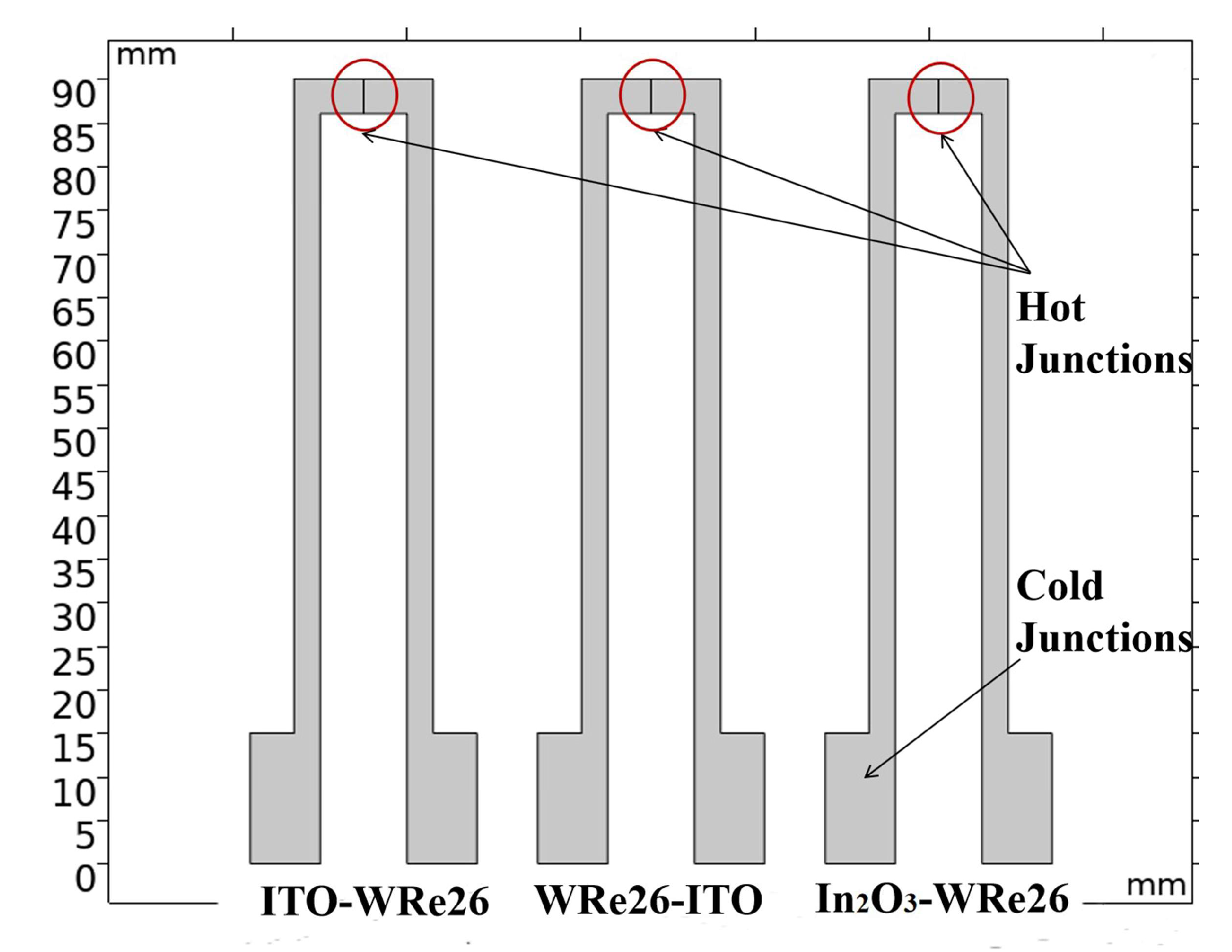
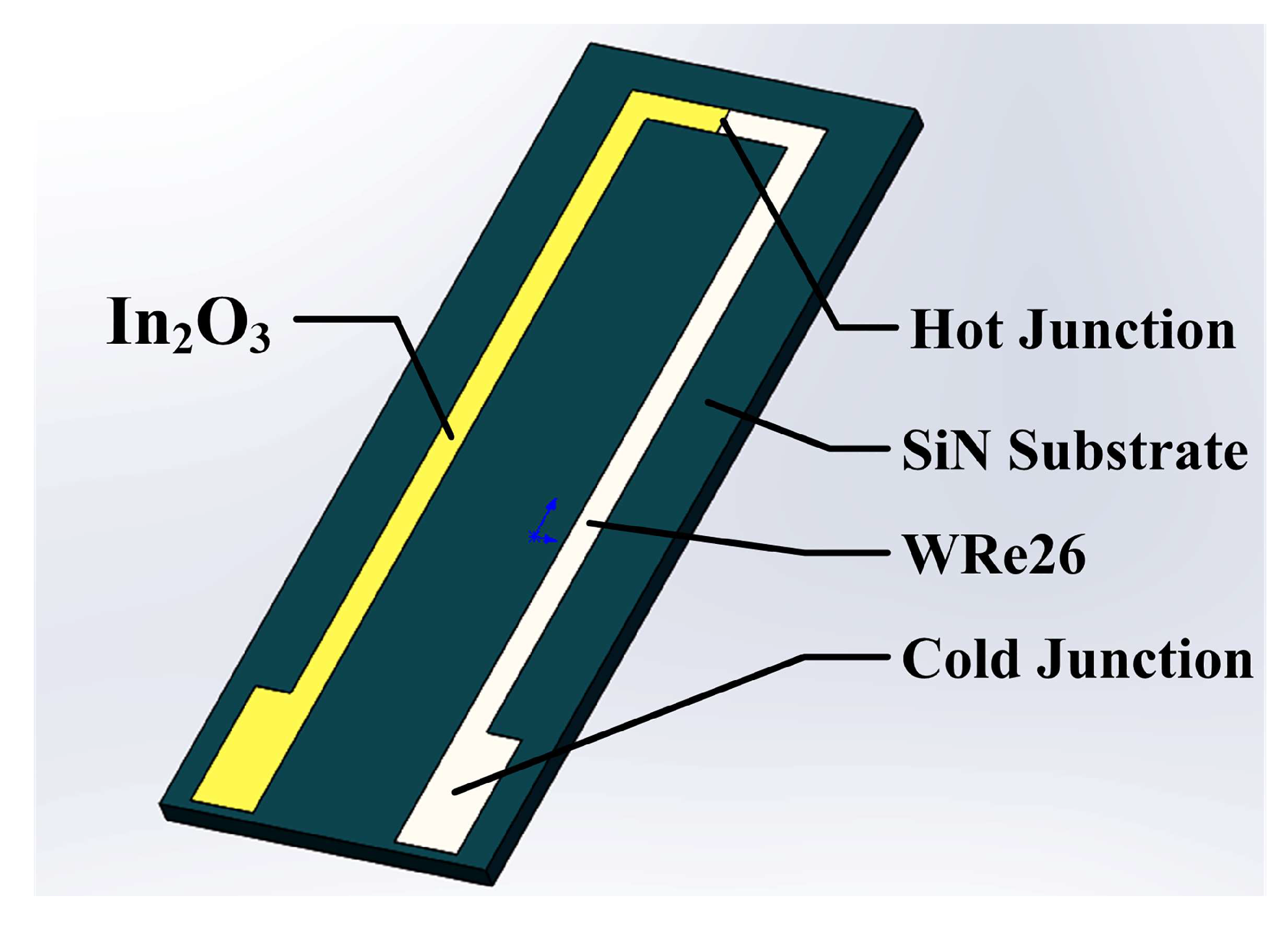
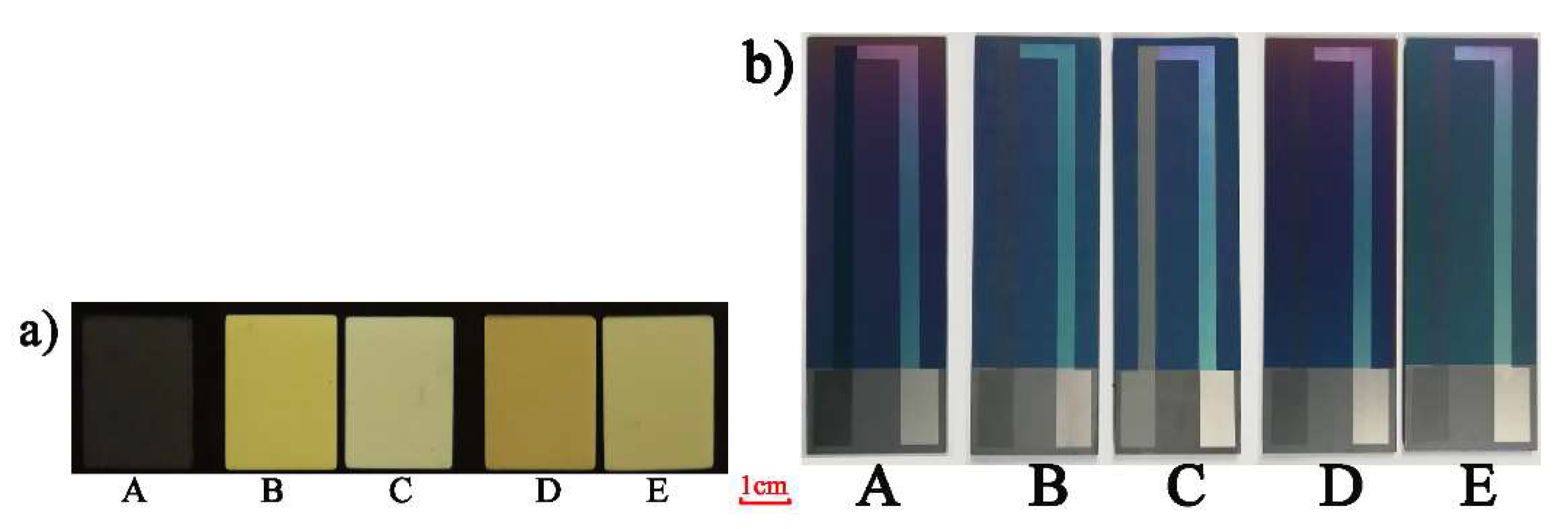
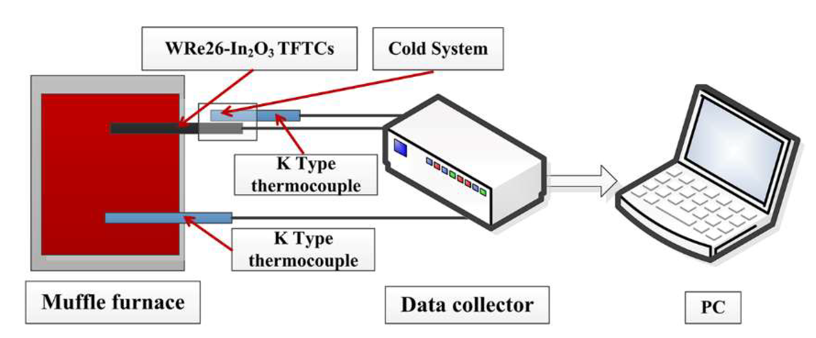
The principle of TFTCs are the same as the traditional wire thermocouples, which is based on the Seebeck effect [25,26]. When the hot junction is heated, and its temperature is T1. And the temperature of cold junction is T0. The thermoelectric potential can be measured at the cold junction of the thermocouples. The thermoelectric voltage of the thin film thermocouple is described as:
E A B = θ 0 θ S A B ( T ) d T = θ 0 θ [ S B ( T ) S A ( T ) ] d T
where the SAB(T) is the Seebeck coefficient of TFTC, SA(T) is the Seebeck coefficient of material A; SB(T) is the Seebeck coefficient of material B, θ is the temperature of hot junction; θ0 is temperature of cold junction.
At the same time, the Seebeck coefficient of the conductive oxides are different from the metals. In2O3 is an N-type non-degenerate semiconductor material. The Seebeck coefficient of In2O3 is gave as:
S ( N D ) = A k e k e I n ( ( 2 π m e * k T ) 2 / 3 h 3 N D )
where S is Seebeck coefficient, K is the Boltzmann constant, h is the Planck constant, e respects electronic charges; ND is carrier concentration, me is effective mass, A is a transport constant [27]. If additional oxygen enters the In2O3, it will affect the Seebeck coefficient of the In2O3. The conductive carriers of In2O3 mainly comes from the electrons released by the oxygen vacancy, and one oxygen vacancy contributes two electrons (Equation (3)) [28]. VO are doubly charged oxygen vacancies. When additional oxygen occupied the oxygen vacancy of the In2O3 film, it caused the carrier concentration in the In2O3 film to decrease while increasing the Seebeck coefficient of the In2O3.
O o x 1 / 2 O 2 + V O + 2 e 1
To verify whether the thermoelectric voltage output of WRe26-In2O3 was better than the pure oxide combination (ITO-In2O3), thermoelectricity simulation of TFTCs with different thermoelectric material combinations was required. The thermoelectric characteristics of the ITO-WRe26, WRe26-In2O3 and ITO-In2O3 TFTCs were studied by using commercial software COMSOL to ensure the results of model analysis. Figure 1 shows the model of the three combinations of TFTCs. The single size of the TFTC is 30 mm × 90 mm. The area of hot junctions is 4 mm × 10 mm. In this analysis, the temperature of hot junctions was increased from 300 K to 1300 K, and the cold junctions were set to 293 K. The Finite Element Analysis results of temperature gradient and thermoelectric voltage distribution are presented in Figure 2. The maximum temperature of the hot junctions are 1300 K. Figure 3 shows the thermoelectric voltage output of TFTCs. According to the simulation results, thermoelectric output of WRe26-In2O3 is the biggest at 1300 K, which means the sensitivity coefficient of this combination is bigger than ITO-In2O3 in theory.

3. Experiment

In order to study the effect of different annealing on the thermoelectric voltage of TFTCs, In2O3 film samples and WRe26-In2O3 TFTCs were prepared by RF magnetron sputtering. RF Magnetron sputtering technology is widely used because of the good adhesion of the films on the substrate, good thickness uniformity and high film density [29,30,31]. High purity WRe26 and In2O3 Target (purity 99.999 wt.%, diameter: 101.6 mm, and thickness: 3 mm) were been used while the distance between target and substrate was 80 mm. In Figure 4, WRe26 and In2O3 films were deposited on the Si3N4 substrate. The mass size of Si3N4 substrate is 30 mm × 90 mm × 3 mm, and the TFTC is 8 mm × 70 mm × 2 um.
Table 1 shows the detail sputtering parameters of the TFTCs preparation. The order of deposition of the two legs of the TFTCs were especially important. The leg of WRe26-In2O3 TFTCs pattern was transferred by using photolithography. In2O3 films deposited by magnetron sputtering for 4 h. Then, In2O3 films were soaked in different annealing processes. After the TFTCs were cleaned up, the WRe26 films were sputtered for 90 min with a high power of 400 w. Finally, the Al2O3 protective layer was covered on the sensitive layer again.
The In2O3 films samples at different annealing processes were presented in Figure 5a. The Al2O3 substrate was 14 mm × 20 mm × 1 mm. The color of film samples obviously changed under different annealing processes. The crystal structure of In2O3 at different annealing conditions was analyzed by X-ray diffraction (XRD), X-ray photoelectron spectroscopy (XPS) was used to characterize its chemical composition. Scanning electron microscopy (SEM) was used to observe the micro-morphology of In2O3 at different annealing conditions, and the WRe26-In2O3 TFTCs were prepared to find the best annealing process by thermoelectric voltage testing (Figure 5b).
Fabricated WRe26-In2O3 TFTCs were static tested in muffle furnace (LHT0820, Nabertherm, Lilienthal, Germany). As shown in Figure 6, one K-type thermocouples and WRe26-In2O3 TFTCs were placed in the muffle furnace to get the temperature of hot junctions. Another K-type was used to monitor the cold junctions. Cold junctions of the TFTCs were cooled by circulating cold water to maintain a big temperature gradient. Then thermoelectric voltage of K-type thermocouples and the WRe26-In2O3 TFTCs were recorded with a data collector (Hioki, LR8410-30, Nagano, Japan).

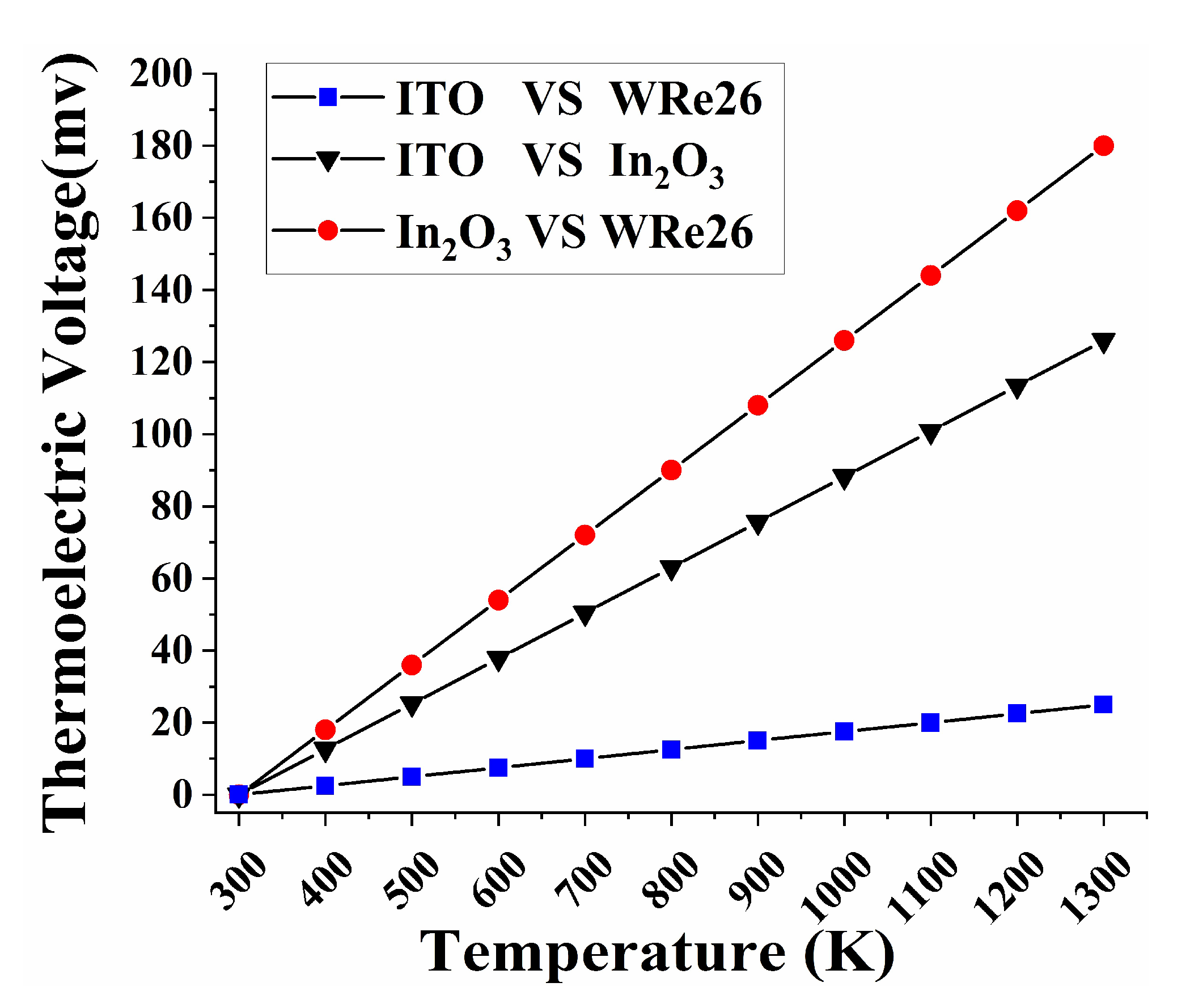
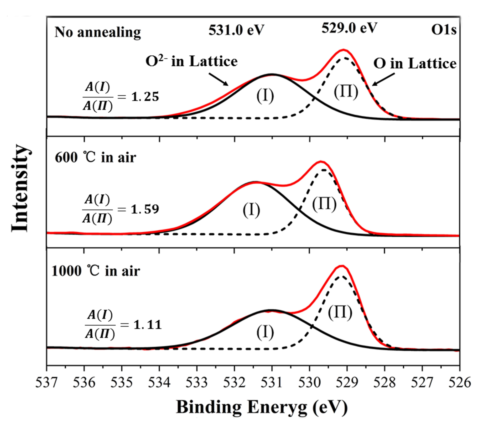
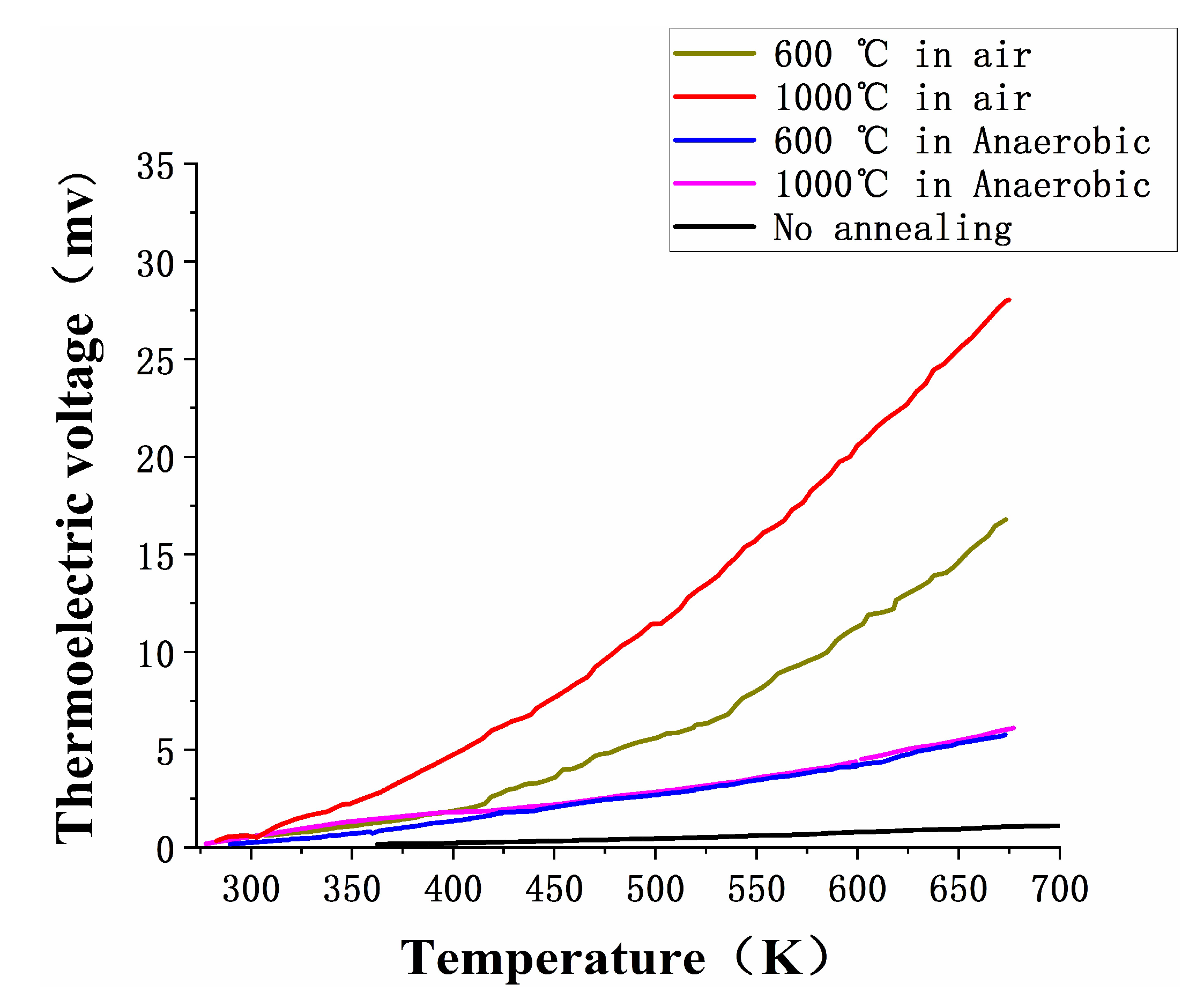
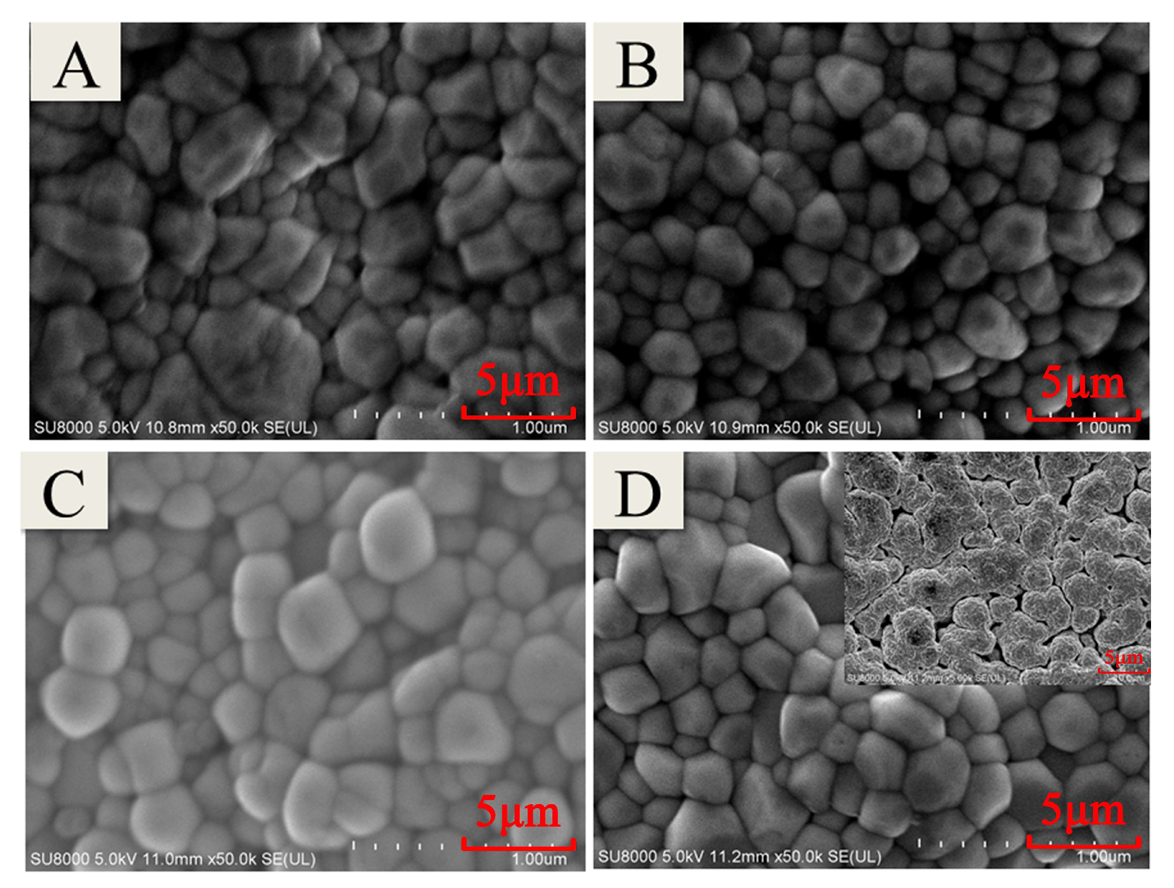
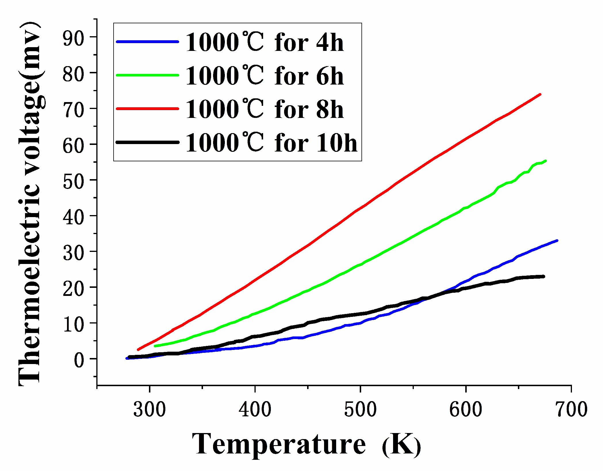
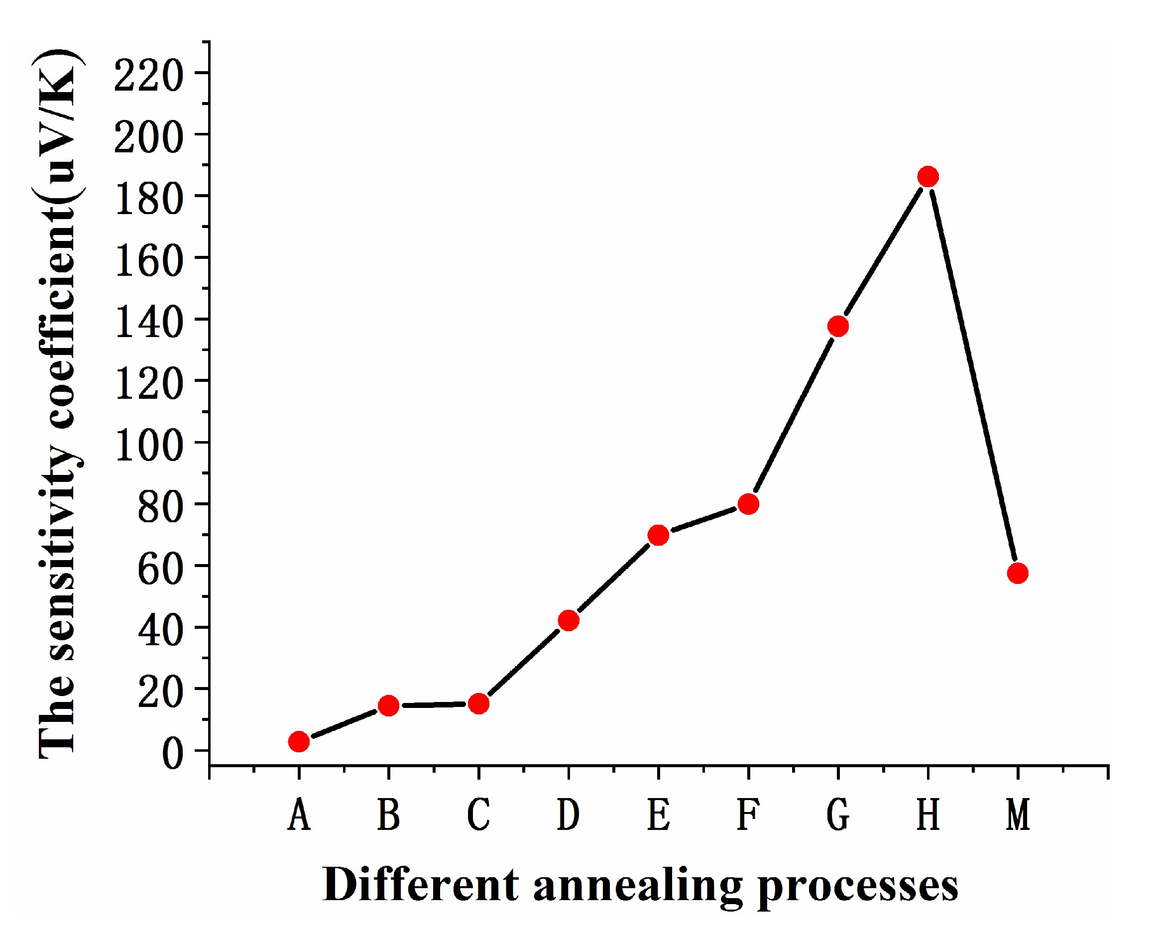
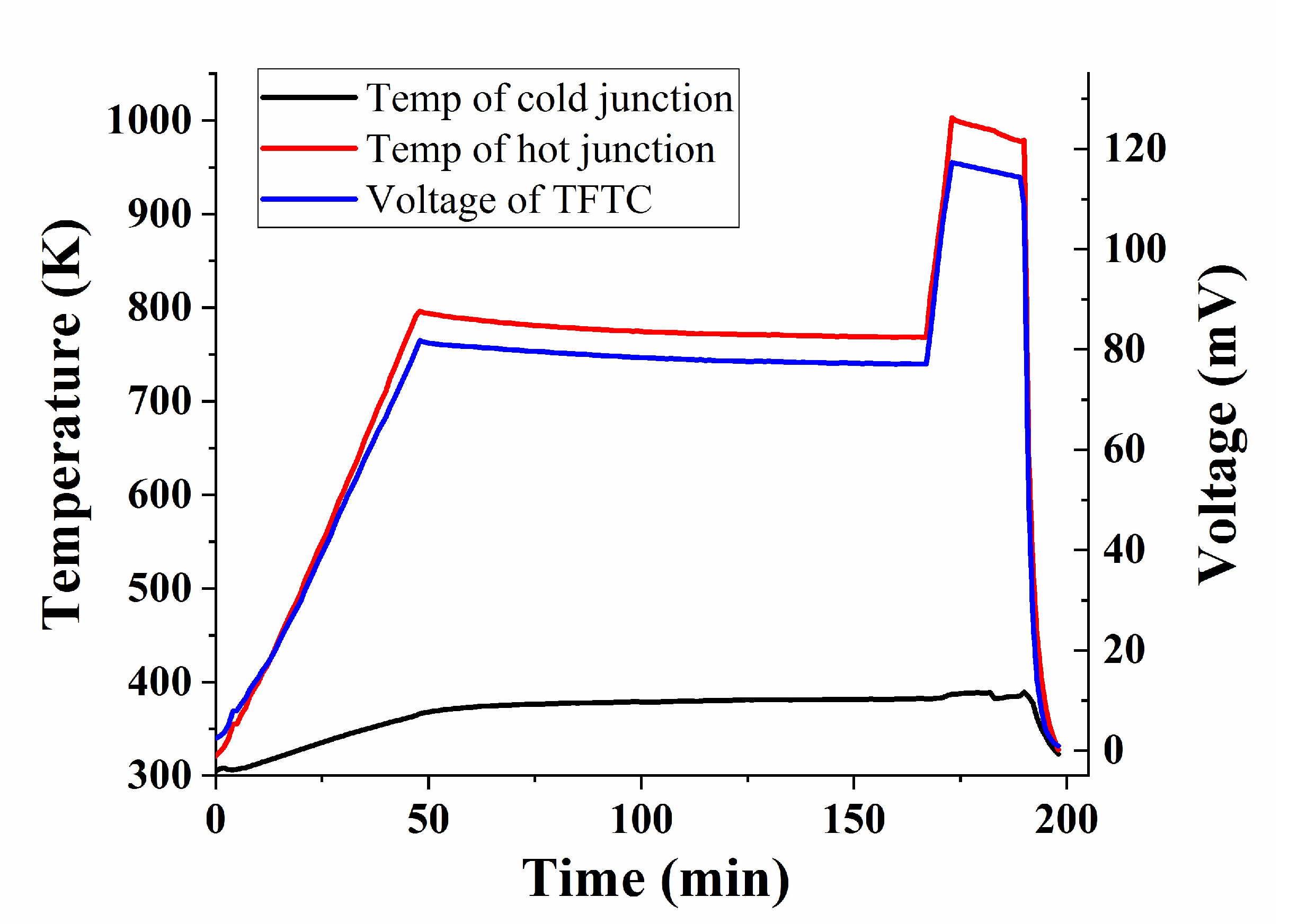
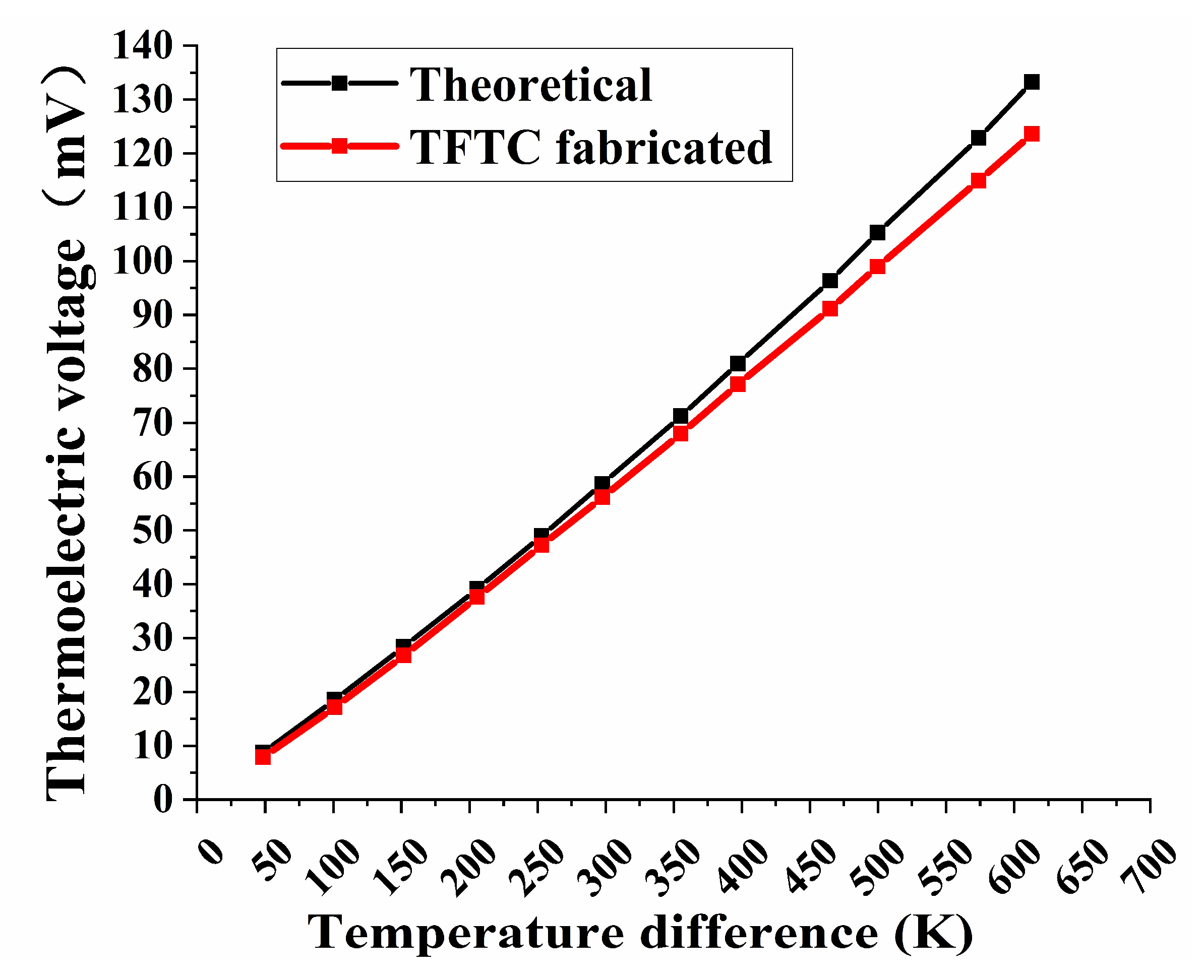
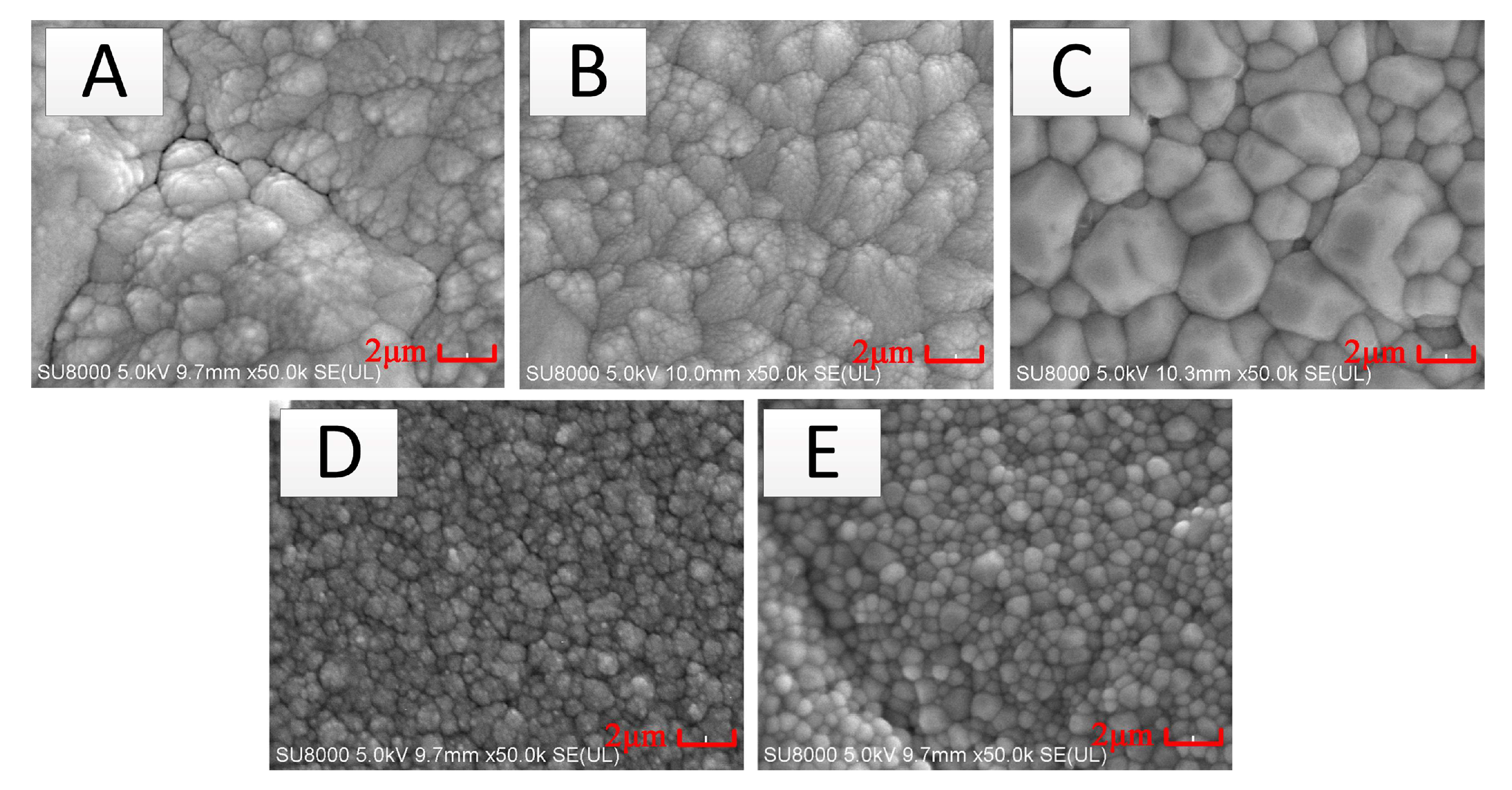
4. Result and Discussion

The X-ray diffraction (XRD) patterns of In2O3 film samples at different annealing process were presented in Figure 7. As shown in Figure 7a, the (222) peak of In2O3 is very small at no annealing. With increasing of air annealing temperature, the (222) and (400) peaks of In2O3 were promoted a great deal, especially the (222) peak increases in the air annealing at 1000 °C. This indicates that the preferred growth of the crystal plane are (222) and (400) crystal planes. In Figure 7b, it was obvious that each peak of In2O3 in XRD was nearly unchanged at the anaerobic annealing processes.
XPS was used to analyze the oxygen element in In2O3 films at different annealing conditions. O 1s core energy spectrum of In2O3 films are shown in Figure 8. The O1s spectrum of In2O3 films has two peaks. The binding energy of 529 eV corresponds to the O element peak and binding energy of 531 eV corresponds to the O2 element peak in In2O3 films. The area ratio under peak of O1s (I) and O1s (II) increased after 600 °C air annealing for 2 h. It is mainly because a large amount of oxygen in the air will not enter the film at a low temperature. Instead, oxygen escaped from the film to produce more oxygen vacancies and the O2− element was increased. Then, In2O3 films recrystallized after annealing at 1000 °C for 2 h. More oxygen entered the In2O3 film, and oxygen vacancy defects were reduced, causing the carrier concentration of In2O3 to be reduced.
Figure 9 exhibits the SEM of the In2O3 films under different annealing conditions. Compared to anaerobic and air annealing, as the temperature increased, the microstructures of In2O3 just became denser at anaerobic annealing. But the microstructures of In2O3 were changed significantly under air annealing. The organization grains of In2O3 became denser and larger, and the cellular crystals were formed at 1000 °C, implying that the oxygen entered the thin film structure at 1000 °C air annealing, and the oxygen occupied the oxygen vacancy of the In2O3 films, making the conductive electrons in the In2O3 film decrease rapidly according to the Equation (3). As a result, the Seebeck coefficient of In2O3 increased.
To verify this phenomenon, Figure 10 shows the result of a static test of TFTCs from room temperature to 673 K at the different annealing process. It is obvious that the thermoelectric voltage was the smallest at no annealing. There were slight changes in the microstructures of In2O3 in 600 °C and 1000 °C anaerobic annealing. The thermoelectric voltage was significantly smaller than air annealing treatment. Thermoelectric voltage at 1000 °C air annealing was much bigger than 600 °C air annealing, which means the Seebeck coefficient of In2O3 films can be improved under air annealing processes, making the performance of WRe26-In2O3 TFTCs better.
In order to find the optimal annealing processes, the In2O3 films were annealed at 1000 °C for a longer time. As shown in Figure 11, with longer time in high temperature annealing, structure grains of In2O3 continued to grow and became more uniform, especially at 10 h. But from the test results of of WRe26-In2O3 TFTCs in Figure 12, it is observed that the thermoelectric voltage output is best at air annealing for 8 h. Thermoelectric voltage output for 10 h is smaller than that for 4 h. The reason was that voids appeared in the In2O3 films (Figure 11d), the grain boundaries of the In2O3 films structure become discontinuous, and the conductivity of the In2O3 films became poor during long duration annealing processes, although oxygen promoted the growth of tissue grains, leading to poor conductivity of the In2O3 film.
The measured thermoelectric voltage depends on the difference between hot junction (Th) and cold junction (Tc) and the Seebeck coefficient of the metal materials. The sensitivity coefficient (S) of thermocouples is given as:
S = Δ V Δ T = Δ V T h T c
where the ΔV is the thermoelectric voltage difference between the WRe26 and In2O3. Figure 13 shows the average sensitivity (The temperature difference was 400K) of WRe26-In2O3 TFTCs at different annealing. The sensitivity coefficient of the TFTCs reached 186.1 μV/K at air annealing for 8 h.
Prepared WRe26-In2O3 TFTC was static calibrated in a high temperature after the optimal annealing process was determined. Figure 14 shows the temperature stability test of TFTC in muffle furnace. The WRe26-In2O3 TFTC and K-type thermocouples were raised from room temperature to 773 K and kept for two hours, and heated to 1000 K for twenty minutes. The heating rate was set at 10 °C/min. Then, TFTC was naturally cooled to room temperature. Figure 15 is a static thermoelectric voltage curve of WRe26-In2O3 TFTCs with the temperature difference up to 612.9 K. The hot junction of the thermocouple was 1000 K (the temperature of cold junction was 387.1 K), the thermoelectric voltage reached 123.6 mv. The average sensitivity coefficient was 201.6 μV/K. We have found the optimal annealing process at this magnetron sputtering process, but the Seebeck coefficient of In2O3 in the literature is about −200 μV/K, and the Seebeck coefficient of WRe26 is about 20 μV/K. So the sensitivity of the WRe26-In2O3 TFTCs is about 220 μV/K in theory. There was a little difference between the prepared TFTC and the theoretical thermoelectric output. This is mainly because the source of the In2O3 target was different, and so the Seebeck coefficient of In2O3 was also a little different. The Seebeck coefficient of In2O3 was highly affected by the quality In2O3 film.

5. Conclusions

In this study, a WRe26-In2O3 TFTC was reported. The WRe26-In2O3 TFTCs were successfully fabricated on the Si3N4 substrate by magnetron sputtering in order to improve the thermoelectric performance of the thermocouple. The properties of In2O3 films and the thermoelectric voltage properties of the WRe26-In2O3 TFTCs under different annealing processes were studied. The properties of In2O3 films at different annealing processes were analyzed by SEM, XRD, and XPS. The optimal annealing process of the TFTCs under this sputtering method was proposed. The WRe26-In2O3 TFTCs had ideal performance at the 1000 °C air annealing for 8 h. It was achieved that the average sensitivity of the WRe26-In2O3 TFTCs could reach 201.6 μV/K at a temperature difference of 612.9 K, which can maintain a stable output for 2 h at 773 K and 20 min for 1000 K.

Author Contributions

Conceptualization, B.T. and Y.L.; methodology, B.T. and Y.L.; software, Z.Z.; validation, Z.Z.; formal analysis, Y.L.; investigation, Z.L., Q.M., P.S., D.L., Q.L.; data curation, Y.L.; writing—original draft preparation, Y.L.; supervision, B.T., L.Z.; project administration, B.T. and Z.J. All authors have read and agreed to the published version of the manuscript.

Funding

This work is supported by National Key Research and Development Project of China (No.2109YFB2004501), Natural Science Foundation of China (No.91748207) and the Fundamental Research Funds for the Central Universities (No. xjj2017018).

Conflicts of Interest

The authors declare no conflict of interest. The funders had no role in the design of the study.

References

  1. Basti, A.; Obikawa, T.; Shinozuka, J. Tools with built-in thin film thermocouple sensors for monitoring cutting temperature. Int. J. Mach. Tools Manuf. 2007, 47, 793–798. [Google Scholar] [CrossRef]
  2. Majumdar, A.; Lai, J.; Chandrachood, M. Thermal imaging by atomic force microscopy using thermocouple cantilever probes. Rev. Sci. Instrum. 1995, 66, 3584. [Google Scholar] [CrossRef]
  3. Leboek, J.; Ali, S.T.; Moller, P. Quantification of in situ temperature measurements on a PBI-based high temperature PEMFC unit cell. Int. J. Hydrog. Energy 2010, 35, 9943–9953. [Google Scholar] [CrossRef]
  4. Aniolek, E.; Gregg, O.J. Thin film thermocouples for advanced ceramic gas turbine engines. Surf. Coat. Technol. 1994, 68, 70–75. [Google Scholar] [CrossRef]
  5. Gregory, O.J.; Amani, M. Stability and microstructure of indium tin oxynitride thin films. J. Am. Ceram. Soc. 2012, 2, 705–710. [Google Scholar] [CrossRef]
  6. ASTM. E230/E230M-12, Standard Specification and Temperature Electromotive Force (emf) Tables for Standardized Thermocouples; ASTM International: West Conshohocken, PA, USA, 2012. [Google Scholar]
  7. Ren, J.; Donovan, D.; Watkins, J. The surface eroding thermocouple for fast heat flux measurement in DIII-D. Rev. Sci. Instrum. 2018, 2018. 89, 10J122. [Google Scholar] [CrossRef]
  8. Chen, Y.Z.; Jiang, H.C. Film thickness influences on the thermoelectric properties of NiCr/NiSi thin film thermocouples. Mod. Phys. Lett. B 2013, 14, 1350103. [Google Scholar] [CrossRef]
  9. Tougas, I.M.; Gregory, O.J. Thin film platinum–palladium thermocouples for gas turbine engine applications. Thin Solid Films 2013, 539, 345–349. [Google Scholar] [CrossRef]
  10. Chen, Y.Z.; Jiang, H.C.; Jiang, S.W.; Liu, X.Z.; Zhang, W.L. Thin film thermocouples for surface temperature measurement of turbine blade. Adv. Mater. Res. 2014, 873, 420–425. [Google Scholar] [CrossRef]
  11. Guo, H.; Jiang, J.Y.; Liu, J.X.; Nie, Z.H.; Ye, F.; Ma, C.F. Fabrication and Calibration of Cu-Ni thin film thermocouples. Adv. Mater. Res. 2012, 512, 2068–2071. [Google Scholar] [CrossRef]
  12. Wrbanek, J.D.; Fralick, G.C. Development of thin film ceramic thermocouples for high tempe-rature environments. In Proceedings of the 40th AIAA/ASME/SAE/ASEE Joint Propulsion Conference and Exhibit. American Institute of Aeronautics and Astronautics, Fort Lauderdale, FL, USA, 11–14 July 2004. [Google Scholar]
  13. Vedula, R.; Desu, S.B.; Fralick, G.C. Thin film TiC/TaC thermocouples. Thin Solid Films 1999, 342, 214–220. [Google Scholar]
  14. Kreider, K. Thin Film High Temperature Silicide Thermocouples. U.S. Patent 5,474,619, 12 December 1995. [Google Scholar]
  15. Liu, Y.; Ren, W.; Shi, P.; Liu, D.; Liu, M.; Jing, W.; Tian, B.; Ye, Z.; Jiang, Z. Preparation and thermal volatility characteristics of In2O3/ITO thin film thermocouple by RF magnetron sputtering. AIP Adv. 2017, 7, 115025. [Google Scholar] [CrossRef] [Green Version]
  16. Chen, X.; Gregory, O.J. Thin-film thermocouples based on the system In2O3–SnO2. J. Am. Ceram. Soc. 2011, 94, 854–860. [Google Scholar] [CrossRef]
  17. Liu, Y.; Ren, W.; Shi, P.; Liu, D.; Zhang, Y.; Liu, M.; Lin, Q.; Tian, B.; Jiang, Z. Microstructure and thermoelectric properties of In2O3/ITO thin film thermocouples with Al2O3 protecting layer. J. Mater. Sci. Mater. Electron. 2018, 30, 1786–1793. [Google Scholar] [CrossRef]
  18. Zhao, X.H.; Ying, K. Stability and thermoelectric properties of ITON: Pt thin film thermocouples. J. Mater. Sci. Mater. Electron. 2016, 27, 1725–1729. [Google Scholar] [CrossRef]
  19. Liu, Y.L.; Ren, W. A highly thermostable In2O3/ITO thin film thermocouple prepared via screen printing for high temperature measurements. Sensors 2018, 18, 958. [Google Scholar] [CrossRef] [Green Version]
  20. Zhao, X.; Li, H.; Chen, Y. Preparation and thermoelectric characteristics of ITO/Pt thin film thermocouples on Ni-based superalloy substrate. Vacuum 2016, 140, 116–120. [Google Scholar] [CrossRef]
  21. Zhang, Y.; Cheng, P. ITO film prepared by ion beam sputtering and its application in high-temperature thermocouple. Vacuum 2017, 146, 31–34. [Google Scholar] [CrossRef]
  22. Tian, B.; Zhang, Z. Tungsten-rhenium thin film thermocouples for sic-based ceramic matrix composites. Rev. Sci. Instrum. 2017, 88, 015007. [Google Scholar] [CrossRef]
  23. Zhang, Z.; Tian, B. Thermoelectric Characteristics of Silicon Carbide and Tungsten-Rhenium-Based Thin-Film Thermocouples Sensor with Protective Coating Layer by RF Magnetron Sputtering. Materials 2019, 12, 1981. [Google Scholar] [CrossRef] [Green Version]
  24. Zhang, Z. Research on Measurement and Process of Tungsten-Rhenium Thin Film Thermocouples Sensor. In Proceedings of the 2018 IEEE 13th Annual International Conference on Nano/Micro Engineered and Molecular Systems (NEMS), Singapore, 22–26 April 2018; pp. 139–142. [Google Scholar]
  25. Molki, A. Simple demonstration of the seebeck effect. Sci. Educ. Rev. 2010, 9, 525–536. [Google Scholar]
  26. Mcaleer, J.F.; Moseley, P.T.; Bourke, P. Tin dioxide gas sensors: Use of the seebeck effect. Sens. Actuators 1985, 8, 251–257. [Google Scholar] [CrossRef]
  27. Jonker, G. The Application of Combined Conductivity and Seebeck Effffect Plots for the Analysis of Semiconductor Properties. Philips Res. Rep. 1968, 23, 131–138. [Google Scholar]
  28. Ellmer, K.; Mientus, R. Carrier Transport in Polycrystalline ITO and ZnO:Al II: The Inflfluence of Grain Barriers and Boundaries. Thin Solid Films 2018, 516, 5829–5835. [Google Scholar] [CrossRef] [Green Version]
  29. Ellmer, K. Magnetron sputtering of transparent conductive zinc oxide: Relation between the sputtering parameters and the electronic properties. J. Phys. D 2000, 33, 4. [Google Scholar] [CrossRef]
  30. Kelly, P.J. Magnetron sputtering: A review of recent developments and applications. Vacuum 2000, 56, 159–172. [Google Scholar] [CrossRef]
  31. Zhang, Z.; Tian, B.; Du, Z. Impact of magnetron sputtering parameters on thermoelectric properties of tungsten-rhenium thin-film thermocouples sensor. IEEE Sens. J. 2018, 24, 9896–9901. [Google Scholar] [CrossRef]
Figure 1. Simulation model of three thermocouple combinations.
Micromachines 11 00664 g001
Figure 2. Simulation of three combinations. (a) The temperature difference distribution of thermocouples. (b) The thermoelectric voltage distribution.
Micromachines 11 00664 g002
Figure 3. Thermoelectric voltage of three combinations simulation results.
Micromachines 11 00664 g003
Figure 4. Structure of WRe26-In2O3 TFTCs.
Micromachines 11 00664 g004
Figure 5. (a) Prepared In2O3 thin film samples at different annealing processes. (b) Prepared TFTCs under different annealing processes. (A: No annealing. B: 600 °Cin air for 2 h. C: 1000 °C in air for 2 h. D: 600 °C in vacuum for 2 h. E: 1000 °C in vacuum for 2 h.).
Micromachines 11 00664 g005
Figure 6. Thermoelectric test system of WRe26-In2O3 TFTCs.
Micromachines 11 00664 g006
Figure 7. X-ray diffraction patterns of In2O3 film under different annealing processes, (a) Annealing process at different temperatures with air environment treatment, (b) Annealing process at different temperatures with vacuum treatment.
Micromachines 11 00664 g007
Figure 8. O1s photoelectron peaks of In2O3 in XPS at different annealing conditions.
Micromachines 11 00664 g008
Figure 9. The SEM of In2O3 films under different annealing processes. (A: No annealing. B: 600 °C in air for 2 h. C: 1000 °C in air for 2 h. D: 600 °C with vacuum for 2 h. E: 1000 °C with vacuum for 2 h.).
Micromachines 11 00664 g009
Figure 10. Thermoelectric voltage output of TFTCs.
Micromachines 11 00664 g010
Figure 11. The SEM of In2O3 films under different annealing processes. (A: 1000 °C in air for 4 h. B: 1000 °C in air for 6 h. C: 1000 °C in air for 8 h. D: 1000 °C in air for 10 h.).
Micromachines 11 00664 g011
Figure 12. Thermoelectric voltage output of TFTCs.
Micromachines 11 00664 g012
Figure 13. Average sensitivity coefficients of TFTCs at different annealing processes. (A: No annealing. B: 600 °C in air for 2 h. C: 1000 °C in air for 2 h. D: 600 °C with vacuum. E: 1000 °C with vacuum. F: 1000 °C in air for 4 h. G: 1000 °C in air for 6 h. H: 1000 °C in air for 8 h. M: 1000 °C in air for 10 h.).
Micromachines 11 00664 g013
Figure 14. Thermoelectric voltage of WRe26-In2O3 TFTCs.
Micromachines 11 00664 g014
Figure 15. Static test thermoelectric voltage and theoretical curve of WRe26-In2O3 TFTCs.
Micromachines 11 00664 g015
Table 1. Sputtering parameters of WRe26-In2O3 TFTCs.
Sputtering ParametersWRe26In2O3Al2O3
Thickness (μm)242
Power (W)400150200
Presser (Pa)1 × 10−61 × 10−65 × 10−5
Ar (sccm)306030

